


方案详情
文
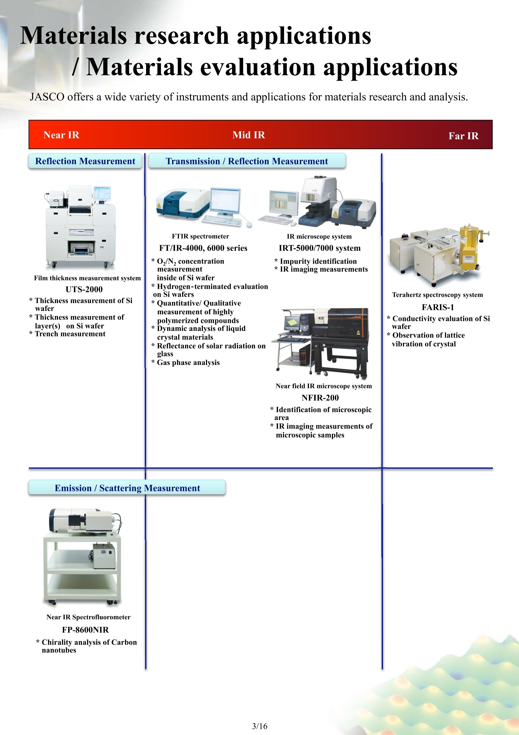
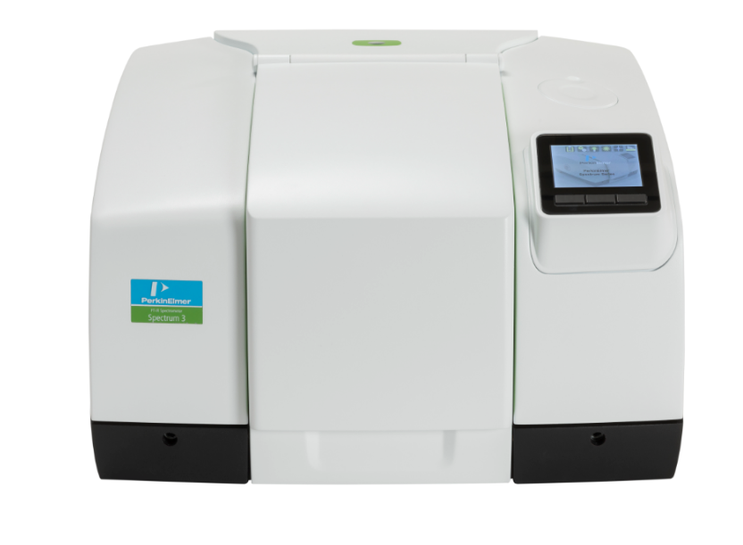
FT/IR-4000, 6000 series?? IRT-5000/7000 system??
* O2/N2 concentration
measurement
inside of Si wafer
* Hydrogen??terminated evaluation
on Si wafers
* Quantitative/ Qualitative
measurement of highly
polymerized compounds ??
* Dynamic analysis of liquid
crystal materials ??
* Reflectance of solar radiation on
glass??
* Gas phase analysis ??
方案详情

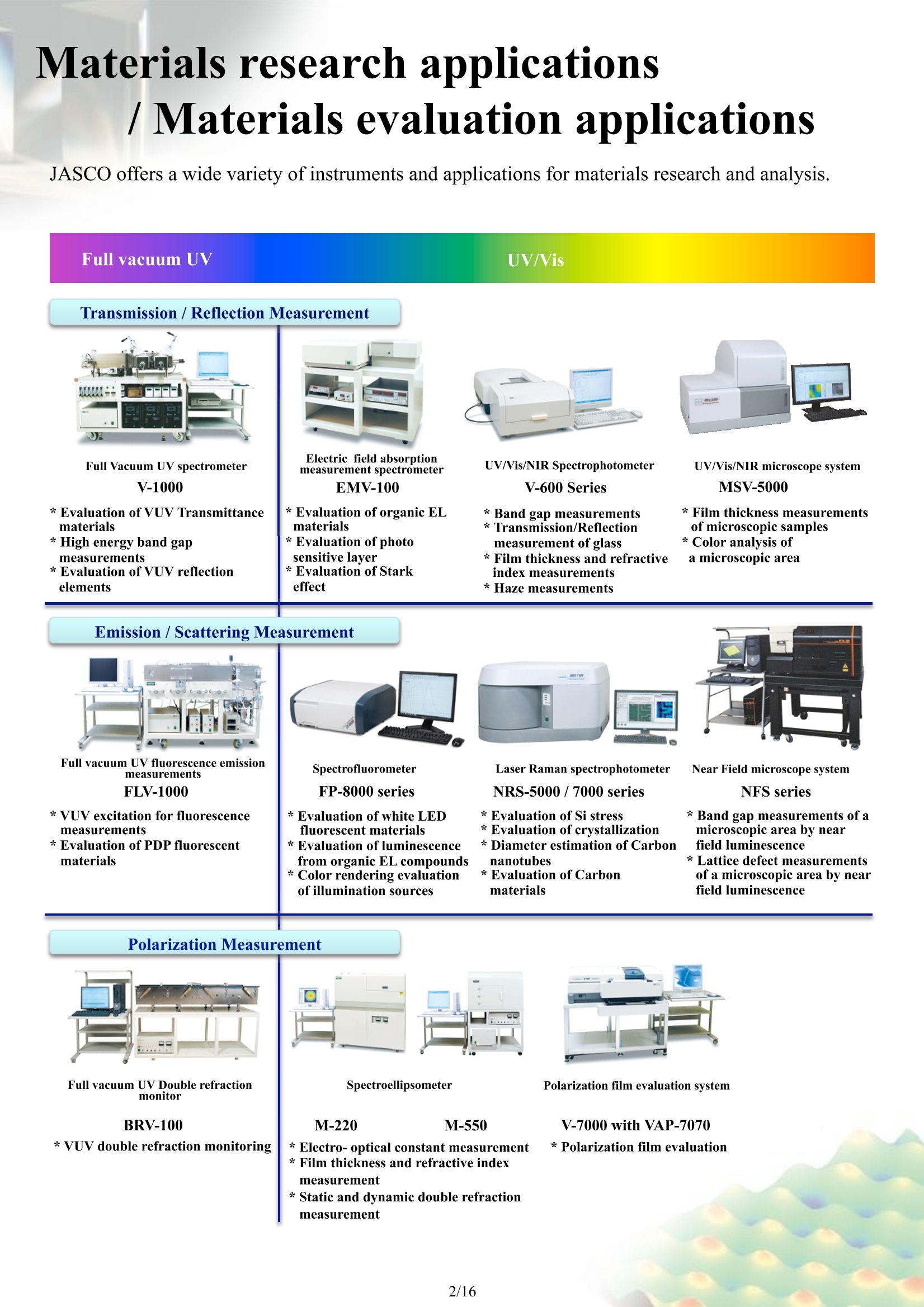
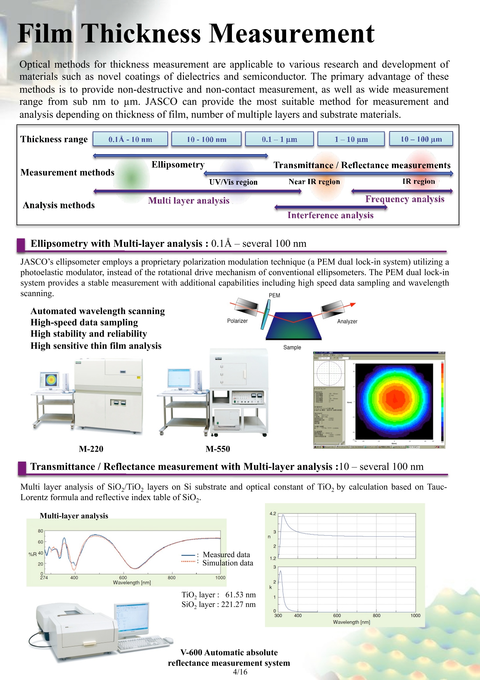
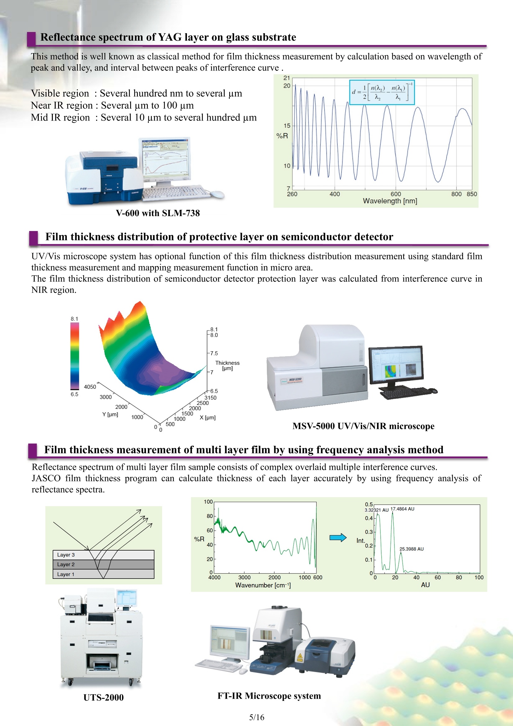
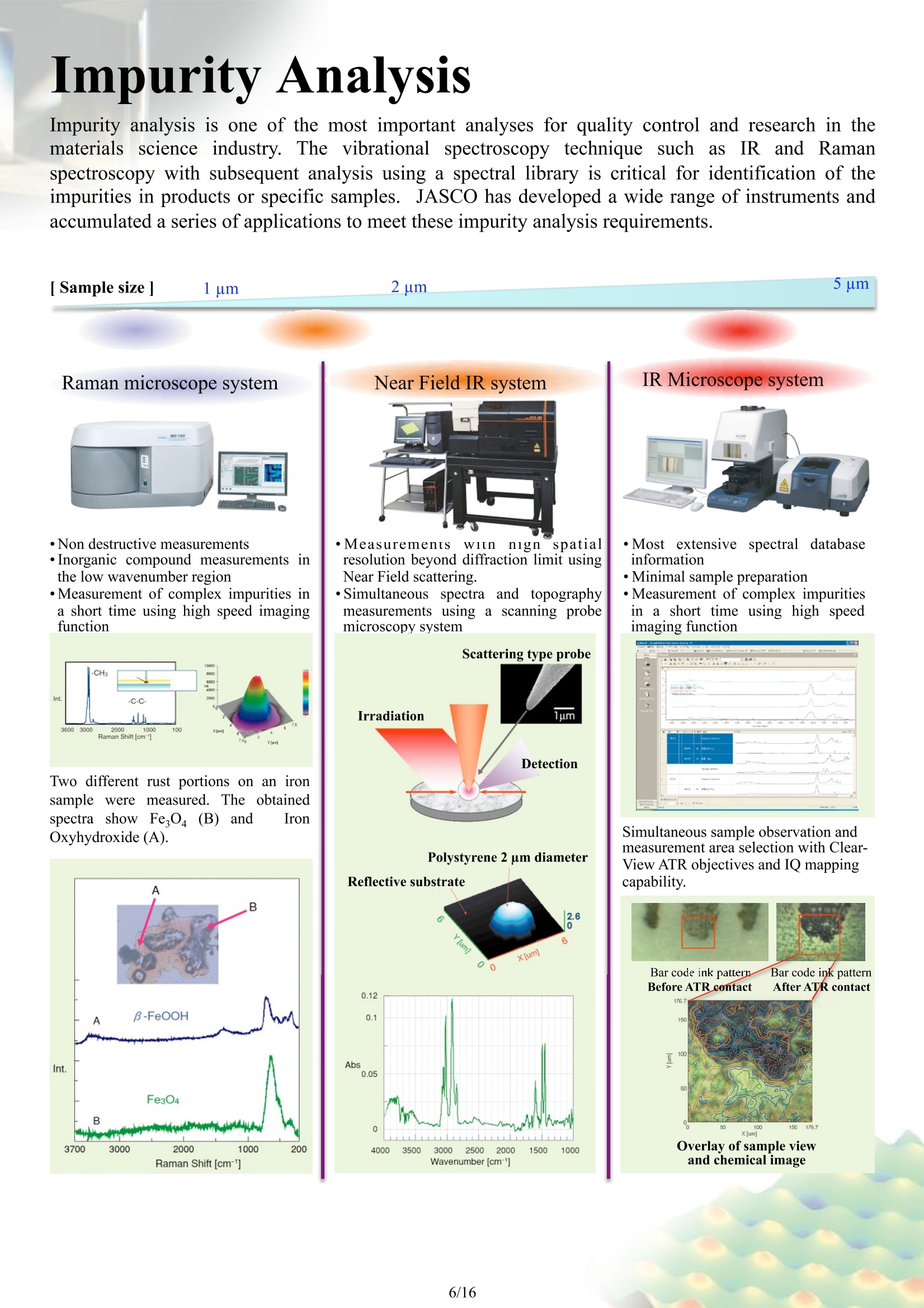
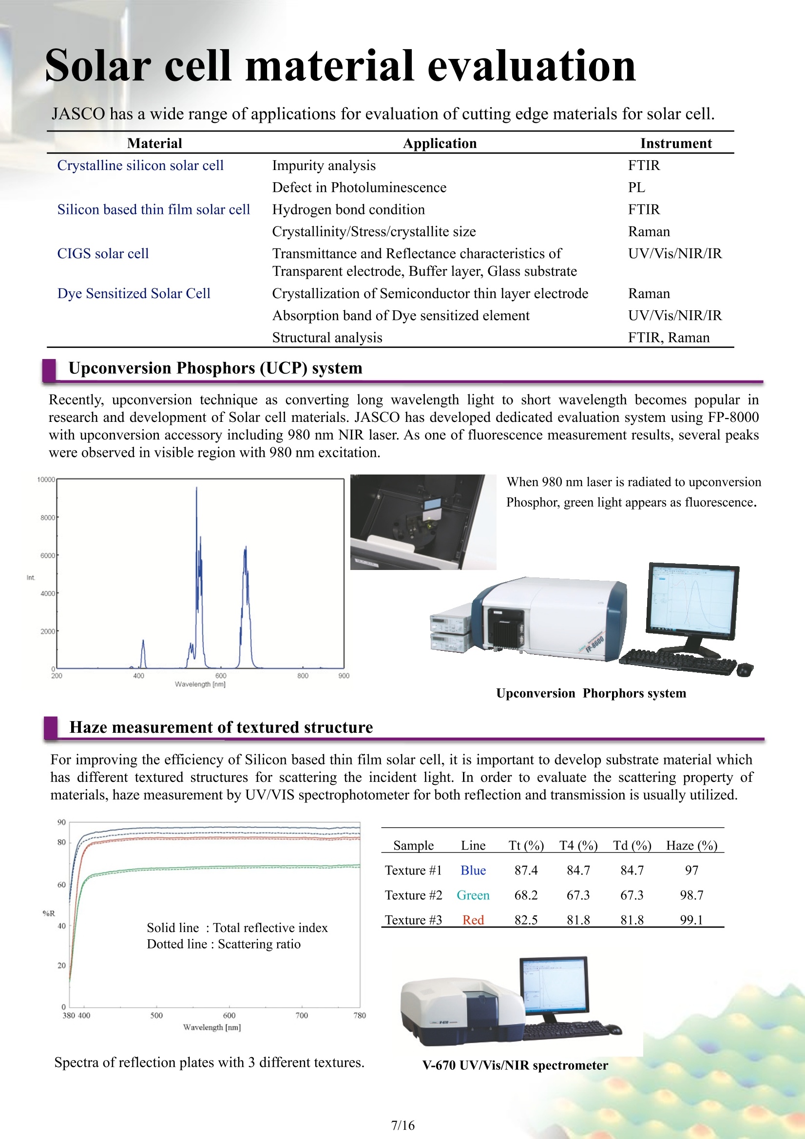
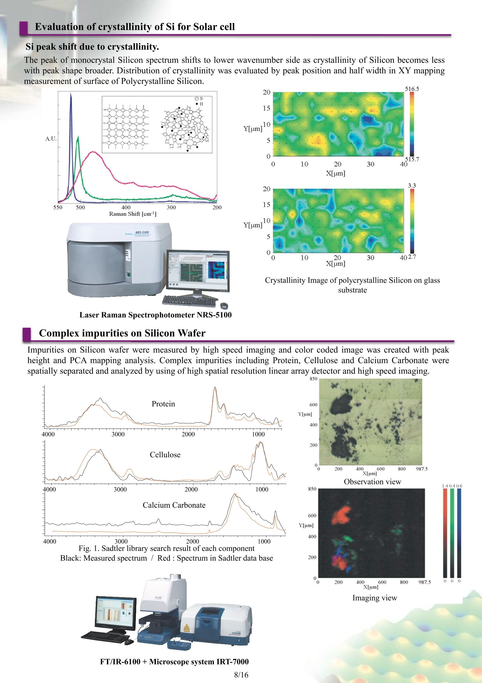
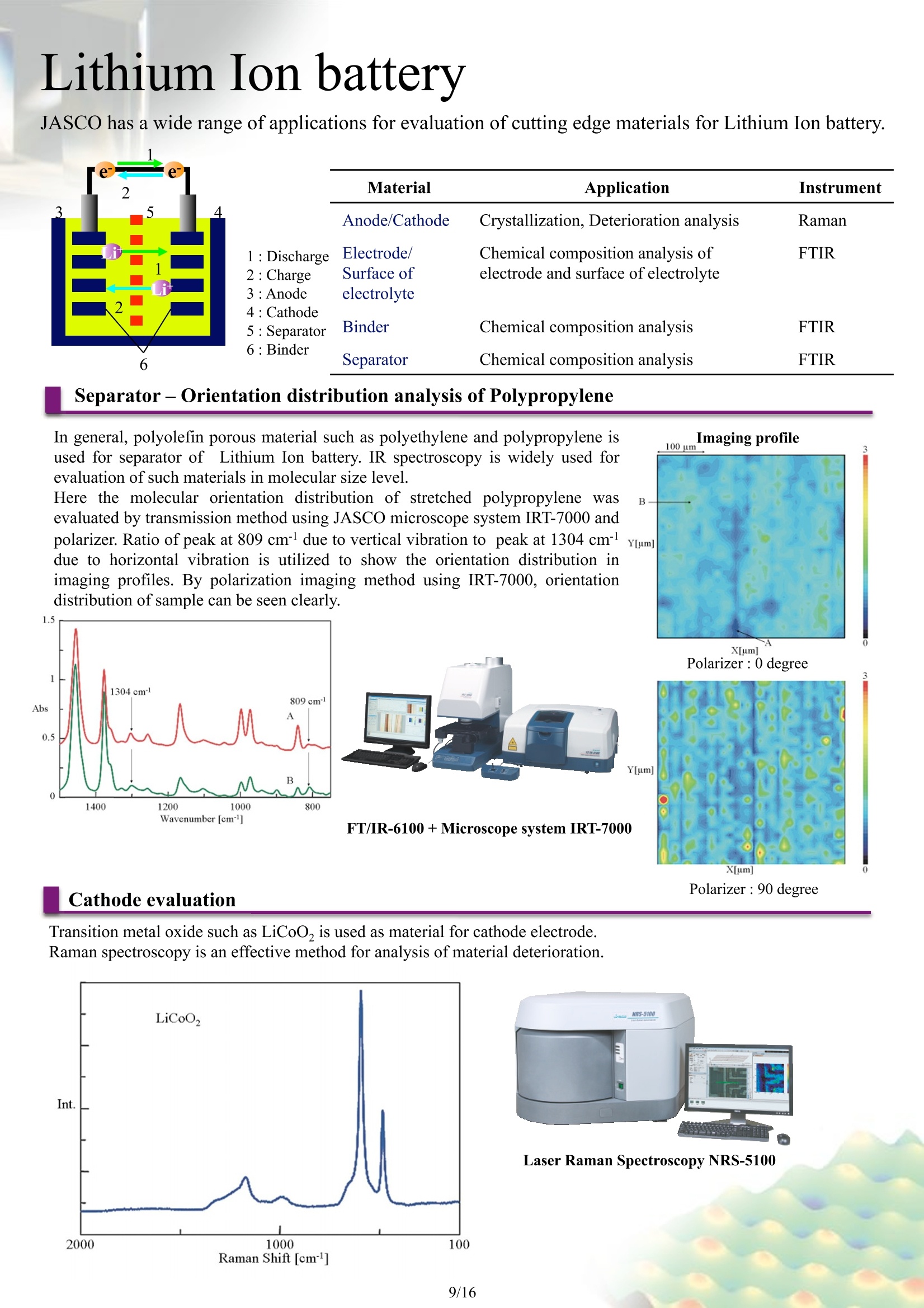
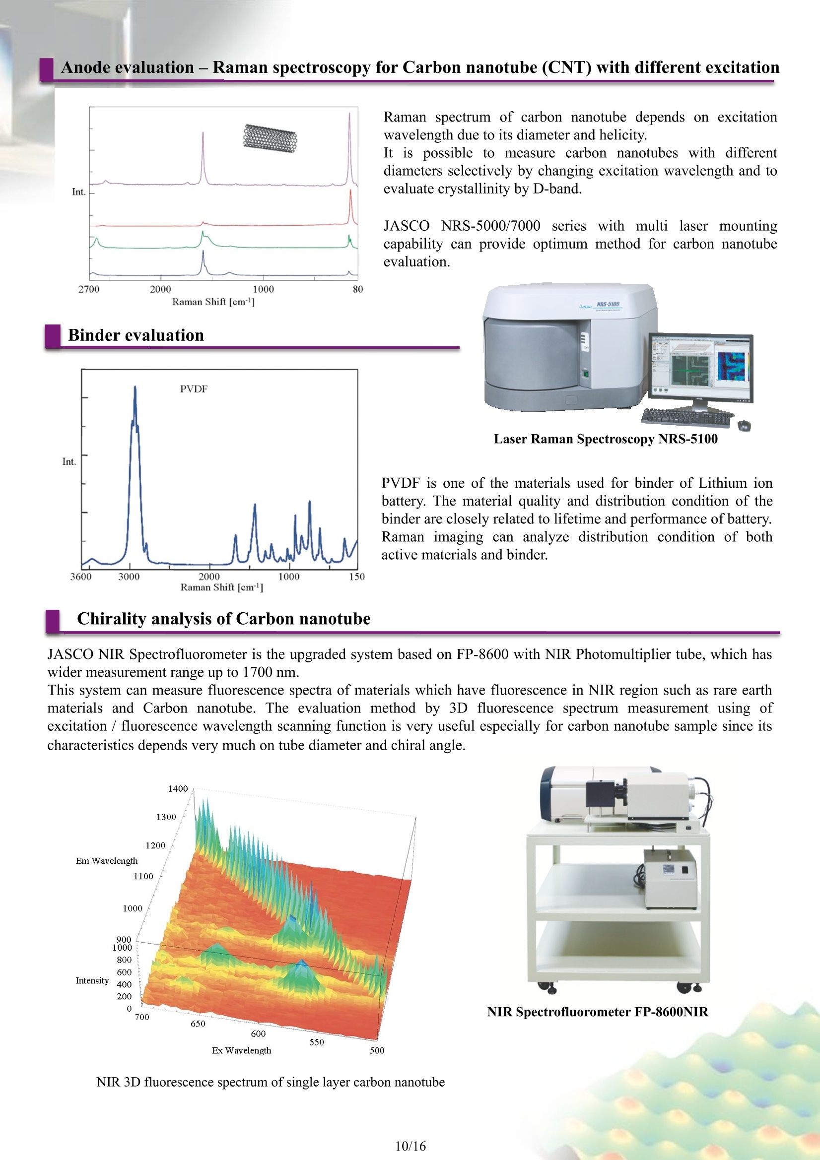
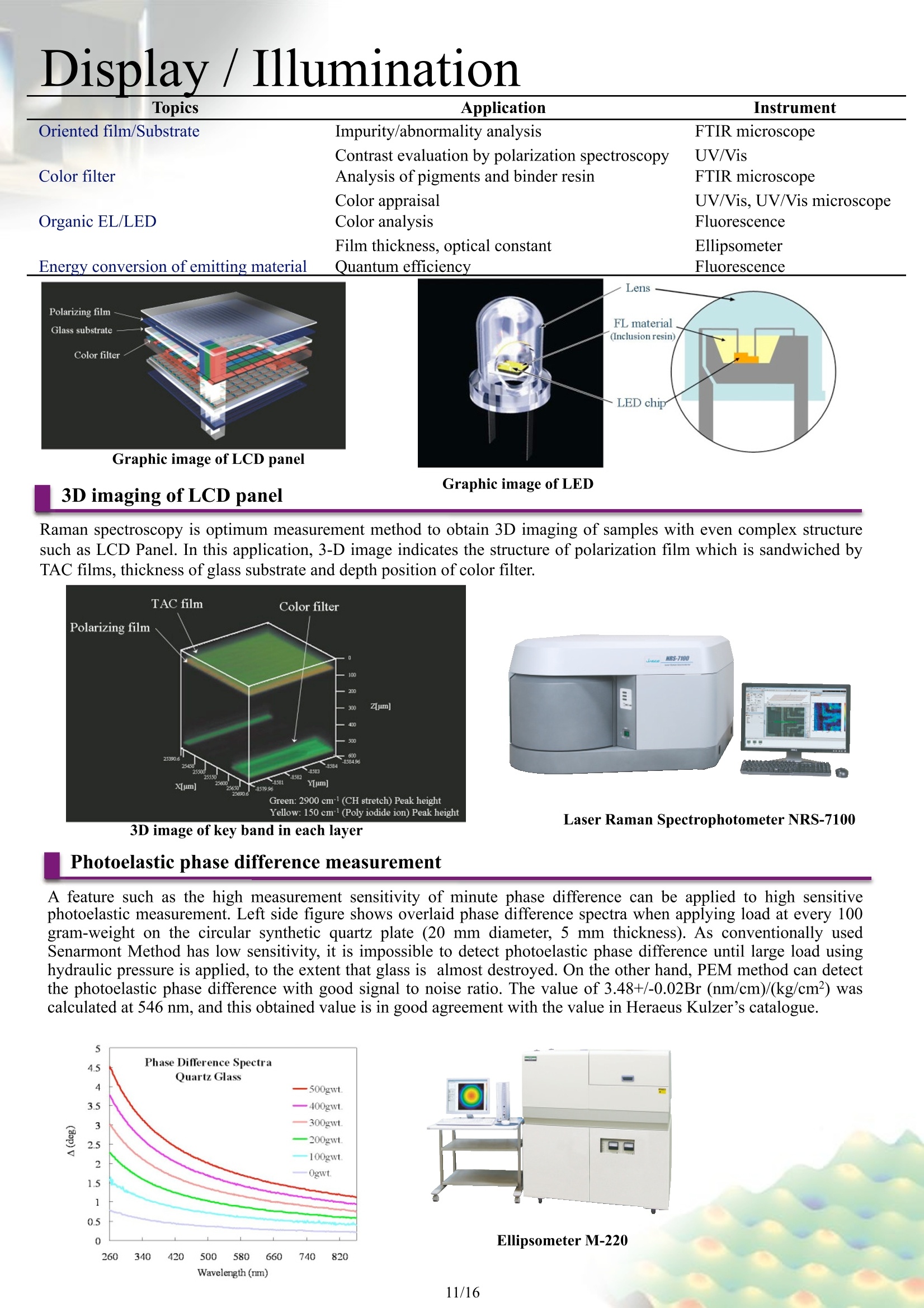
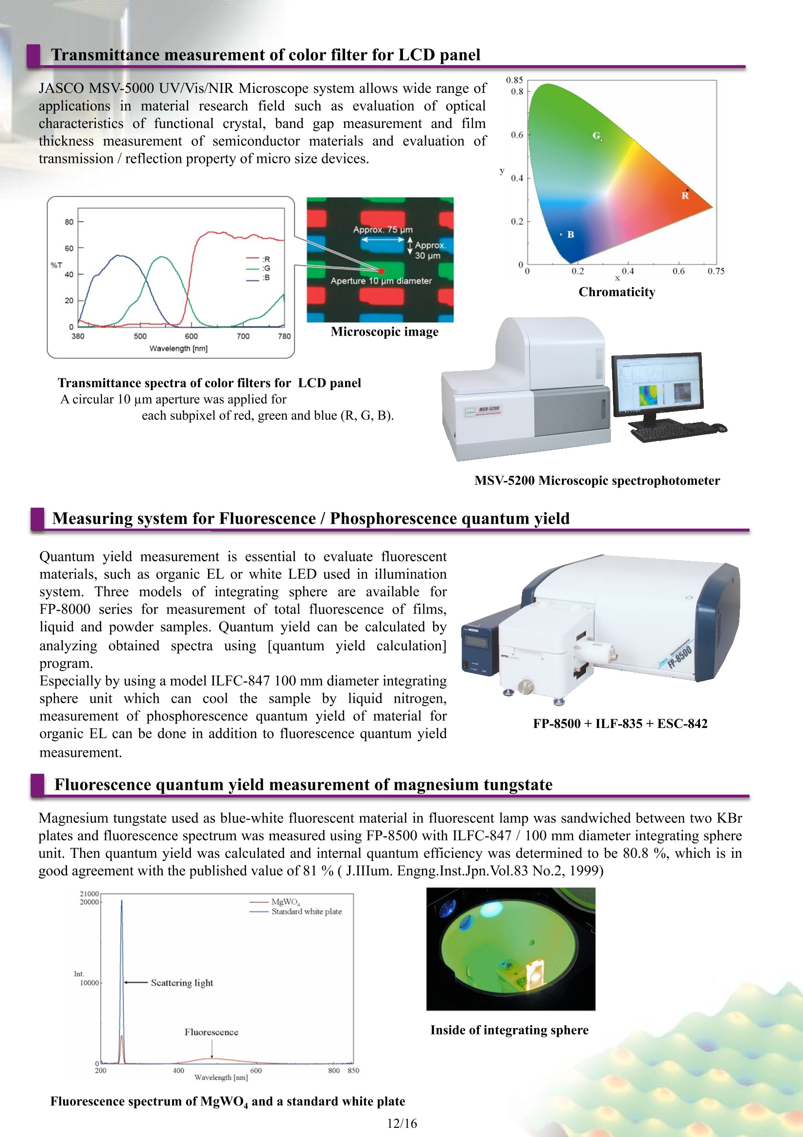
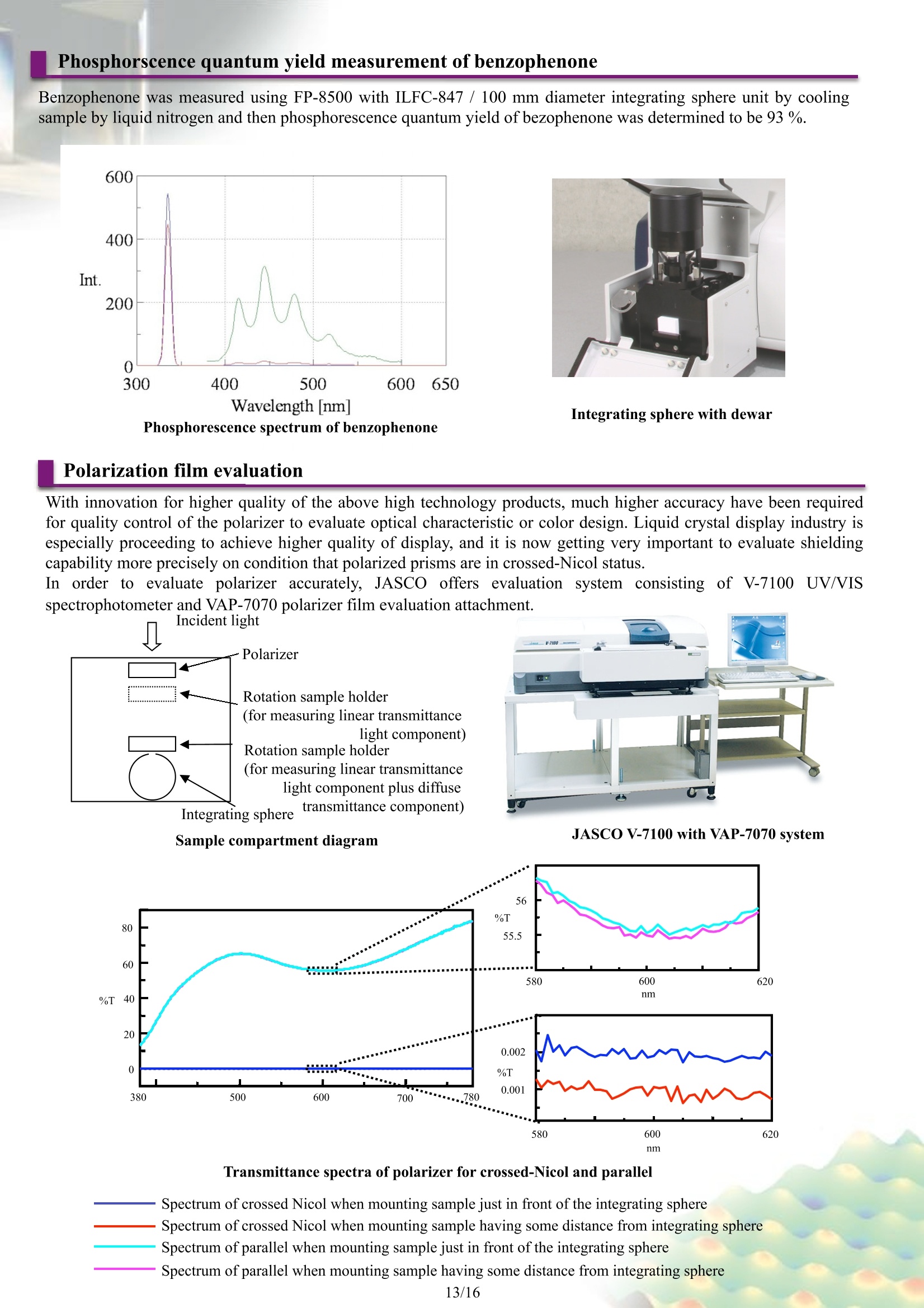
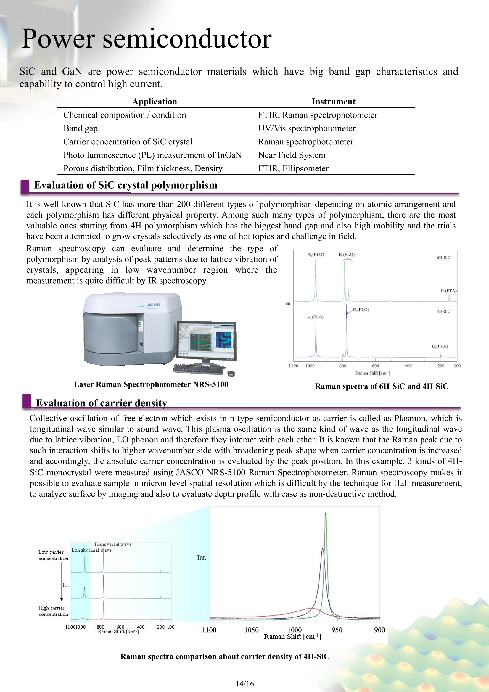
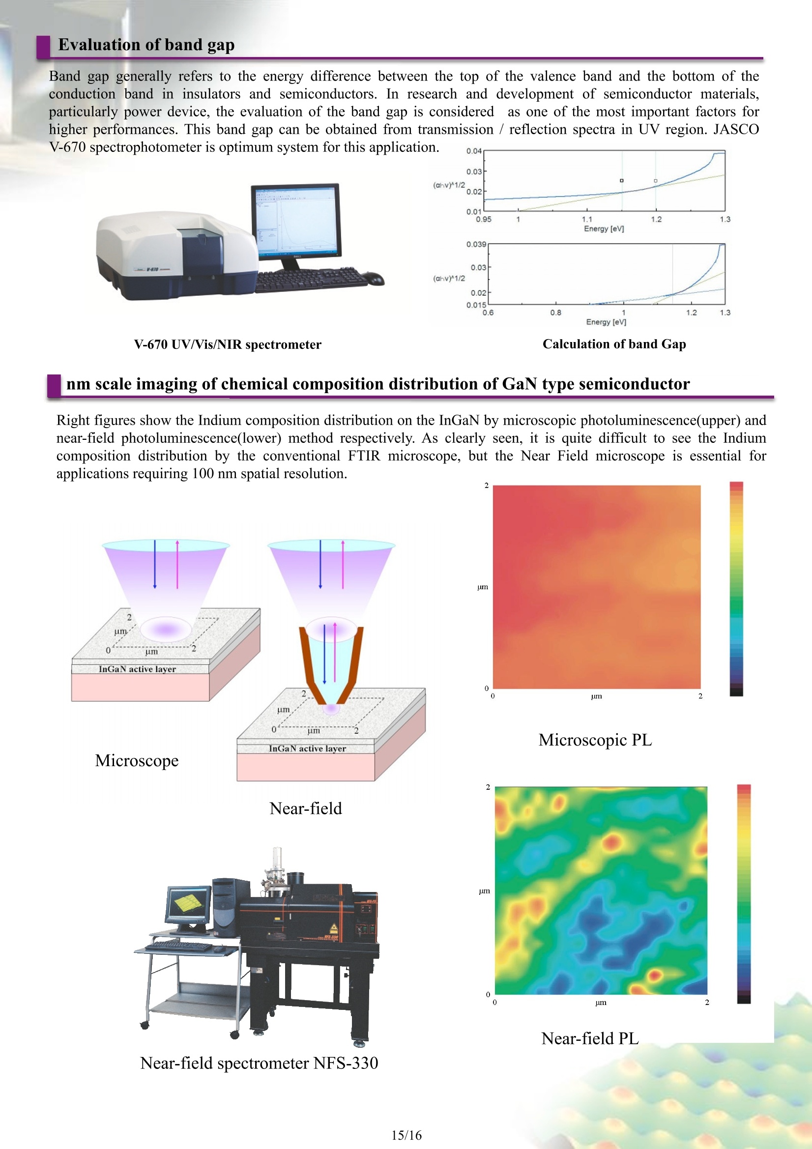
Evaluation of crystallinity of Si for Solar cell Anode evaluation - Raman spectroscopy for Carbon nanotube (CNT) with different excitation Applications andSolutions For Research and Developmentin Material and Semiconductor field Materials research applications/ Materials evaluation applications JASCO offers a wide variety of instruments and applications for materials research and analysis. Fullvacuum UV UV/Vis * Evaluation of VUV Transmittancematerials * High energy band gap measurements elements Emission/Scattering Measurement Full vacuum UV fluorescence emissionmeasurementsFLV-1000 SpectrofluorometerFP-8000 series Laser Raman spectrophotometerNRS-5000/7000 series Near Field microscope system NFS series * VUV excitation for fluorescencemeasurements *Evaluation of white LED * Evaluation of Si stress * Band gap measurements of a fluorescent materials * Evaluation of crystallization microscopic area by near * Evaluation of PDP fluorescentmaterials * Evaluation of luminescence * Diameter estimation of Carbon field luminescence from organic EL compounds nanotubes * Lattice defect measurements *Colorrendering evaluation * Evaluation of Carbon of a microscopic area by near of illumination sources materials field luminescence Polarization Measurement Full vacuum UV Double refractionmonitor Polarization film evaluation system BRV-100 V-7000 with VAP-7070 * VUV double refraction monitoring *Electro-optical constant measurement* Film thickness and refractive indexmeasurement *Polarization film evaluation * Static and dynamic double refraction measurement Materials research applications/Materials evaluation applications JASCO offers a wide variety of instruments and applications for materials research and analysis. Film Thickness Measurement Optical methods for thickness measurement are applicable to various research and development ofmaterials such as novel coatings of dielectrics and semiconductor. The primary advantage of thesemethods is to provide non-destructive and non-contact measurement, as well as wide measurementrange from sub nm to um. JASCO can provide the most suitable method for measurement andanalysis depending on thickness of film, number of multiple layers and substrate materials. Thickness range 0.1A-10nm 10-100 nm 0.1-1pm 1-10 um 10-100um Ellipsometry Transmittance/Reflectance measurements Measurement methods UV/Vis region Near IR region IR region Analysis methods Multi layer analysisFrequency analysis Interference analysis Ellipsometry with Multi-layer analysis : 0.1A -- several 100 nm JASCO's ellipsometer employs a proprietary polarization modulation technique (a PEM dual lock-in system) utilizing aphotoelastic modulator, instead of the rotational drive mechanism of conventional ellipsometers. The PEM dual lock-insystem provides a stable measurement with additional capabilities including high speed data sampling and wavelengthscanning. PEM Transmittance /Reflectance measurement with Multi-layer analysis :10 - several 100 nm Multi layer analysis of SiO,/TiO, layers on Si substrate and optical constant of TiO,by calculation based on Tauc-Lorentz formula and reflective index table of SiO,. Reflectance spectrum of YAG layer on glass substrate This method is well known as classical method for film thickness measurement by calculation based on wavelength ofpeak and valley, and interval between peaks of interference curve. Visible region : Several hundred nm to several umNear IR region : Several um to 100 umMid IR region : Several 10 um to several hundred um V-600 with SLM-738 Film thickness distribution of protective layer on semiconductor detector UV/Vis microscope system has optional function of this film thickness distribution measurement using standard filmthickness measurement and mapping measurement function in micro area. The film thickness distribution of semiconductor detector protection layer was calculated from interference curve inNIR region. MSV-5000 UV/Vis/NIR microscope Film thickness measurement of multi layer film by using frequency analysis method Reflectance spectrum of multi layer film sample consists of complex overlaid multiple interference curves.JASCO film thickness program can calculate thickness of each layer accurately by using frequency analysis ofreflectance spectra. UTS-2000 FT-IR Microscope system Impurity Analysis Impurity analysis is one of the most important analyses for quality control and research in thematerialsscience industry. The vibrational spectroscopy technique such as IR and Ramanspectroscopy with subsequent analysis using a spectral library is critical for identification of theimpurities in products or specific samples.JASCO has developed a wide range of instruments andaccumulated a series of applications to meet these impurity analysis requirements. [Sample size ] 11um 2 um 5um Raman microscope system ·Non destructive measurements ·Inorganic compound measurements inthe low wavenumber region ·Measurement of complex impurities ina short time using high speed imagingfunction Two different rust portions on an ironsamplee were measured. The obtainedspectra show Fe04 (B) and IronOxyhydroxide(A). A .B A B-FeOOH Int. Fe3O4 B 一w 3700 3000 2000 1000 200 0 4000 3500 30002500 2000 1500 1000 Wavenumber [cm'] IR Microscope system ·Most extensiveespectral idatabaseinformation ·Minimal sample preparation ·Measurement of complex impurities in a short time using high speed imaging function .n.... Simultaneous sample observation andmeasurement area selection with Clear-View ATR objectives and IQ mappingcapability. Overlay of sample viewand chemical image Solar cellrmaterial evaluation JASCO has a wide range of applications for evaluation of cutting edge materials for solar cell. Material Application Instrument Crystalline silicon solar cell Impurity analysis FTIR Defect in Photoluminescence PL Silicon based thin film solar cell Hydrogen bond condition FTIR Crystallinity/Stress/crystallite size Raman CIGS solar cell Transmittance and Reflectance characteristics of Transparent electrode, Buffer layer, Glass substrate UV/Vis/NIR/IR Dye Sensitized Solar Cell Crystallization of Semiconductor thin layer electrode Raman Absorption band of Dye sensitized element UV/Vis/NIR/IR Structural analysis FTIR, Raman Upconversion Phosphors (UCP) system Recently, upconversion technique as converting long wavelength light to short wavelength becomes popular inresearch and development of Solar cell materials. JASCO has developed dedicated evaluation system using FP-8000with upconversion accessory including 980 nm NIR laser. As one of fluorescence measurement results, several peakswere observed in visible region with 980 nm excitation. Haze measurement of textured structure For improving the efficiency of Silicon based thin film solar cell, it is important to develop substrate material whichhas different textured structures for scattering the incident light. In order to evaluate the scattering property ofmaterials, haze measurement by UV/VIS spectrophotometer for both reflection and transmission is usually utilized. Sample Line Tt (%) T4(%) Td (%) Haze (%) Texture #1 Blue 87.4 84.7 84.7 97 Texture #2 Green 68.2 67.3 67.3 98.7 Texture #3 Red 82.5 81.8 81.8 99.1 Spectra of reflection plates with 3 different textures. V-670 UV/Vis/NIR spectrometer The peak of monocrystal Silicon spectrum shifts to lower wavenumber side as crystallinity of Silicon becomes lesswith peak shape broader. Distribution of crystallinity was evaluated by peak position and half width in XY mappingmeasurement of surface of Polycrystalline Silicon. 400Raman Shift [cm] Laser Raman Spectrophotometer NRS-5100 Complex impurities on Silicon Wafer X[um] Crystallinity Image of polycrystalline Silicon on glasssubstrate Black: Measured spectrum / Red: Spectrum in Sadtler data base FT/IR-6100 +Microscope system IRT-7000 850 Observation view Imaging view Lithium Ion battery JASCO has a wide range of applications for evaluation of cutting edge materials for Lithium Ion battery. Material Application Instrument Anode/Cathode Crystallization, Deterioration analysis Raman Electrode/ Chemical composition analysis of FTIR Surface of electrode and surface ofelectrolyte electrolyte Binder Chemical composition analysis FTIR Separator Chemical composition analysis FTIR Separator-Orientation distribution analysis of Polypropylene In general, polyolefin porous material such as polyethylene and polypropylene isused for separator of Lithium Ion battery. IR spectroscopy is widely used forevaluation of such materials in molecular size level. Here the molecular orientation distribution of stretched polypropylene wasevaluated by transmission method using JASCO microscope system IRT-7000 andpolarizer. Ratio of peak at 809 cm due to vertical vibration to peak at 1304 cmdue to horizontal vibration is utilized to show the orientation distribution inimaging profiles. By polarization imaging method using IRT-7000, orientationdistribution of sample can be seen clearly. X[um] Polarizer : 0 degree FT/IR-6100+Microscope system IRT-7000 0 Polarizer : 90 degree Cathode evaluation Transition metal oxide such as LiCoO, is used as material for cathode electrode.Raman spectroscopy is an effective method for analysis of material deterioration. Laser Raman Spectroscopy NRS-5100 Raman Shift [cm] It is possible to measure carbon nanotubes with differentdiameters selectively by changing excitation wavelength and toevaluate crystallinity by D-band. JASCO NRS-5000/7000 seriesVwith multi laser mountingcapability can provide optimum method for carbon nanotubeevaluation. Laser Raman Spectroscopy NRS-5100 PVDF is one of the materials used for binder of Lithium ionbattery. The material quality and distribution condition of thebinder are closely related to lifetime and performance of battery.Raman imaging can analyze distribution condition of bothactive materials and binder. Chirality analysis of Carbon nanotube JASCO NIR Spectrofluorometer is the upgraded system based on FP-8600 with NIR Photomultiplier tube, which haswider measurement range up to 1700 nm. This system can measure fluorescence spectra of materials which have fluorescence in NIR region such as rare earthmaterials and Carbon nanotube. The evaluation method by 3D fluorescence spectrum measurement using ofexcitation / fluorescence wavelength scanning function is very useful especially for carbon nanotube sample since itscharacteristics depends very much on tube diameter and chiral angle. Topics Application Instrument Oriented film/Substrate Impurity/abnormality analysis FTIR microscope Contrast evaluation by polarization spectroscopy UV/Vis Color filter Analysis of pigments and binder resin FTIR microscope Color appraisal UV/Vis,UV/Vis microscope Organic EL/LED Color analysis Fluorescence Film thickness, optical constant Ellipsometer Energy conversion of emitting material Quantum efficiency Fluorescence Lens Graphic image of LED 3D imaging of LCD panel Raman spectroscopy is optimum measurement method to obtain 3D imaging of samples with even complex structuresuch as LCD Panel. In this application, 3-D image indicates the structure of polarization film which is sandwiched byTAC films, thickness of glass substrate and depth position of color filter. Laser Raman Spectrophotometer NRS-7100 3D image of key band in each layer Photoelastic phase difference measurement A feature such as the high measurement sensitivity of minute phase difference can be applied to high sensitivephotoelastic measurement. Left side figure shows overlaid phase difference spectra when applying load at every 100gram-weight on the circular synthetic quartz plate (20 mm diameter, 5 mm thickness). As conventionally usedSenarmont Method has low sensitivity, it is impossible to detect photoelastic phase difference until large load usinghydraulic pressure is applied, to the extent that glass is almost destroyed. On the other hand, PEM method can detectthe photoelastic phase difference with good signal to noise ratio. The value of 3.48+/-0.02Br (nm/cm)/(kg/cm²) wascalculated at 546 nm, and this obtained value is in good agreement with the value in Heraeus Kulzer’s catalogue. Ellipsometer M-220 JASCO MSV-5000 UV/Vis/NIR Microscope system allows wide range ofapplications in material research field such as evaluation of opticalcharacteristics of functional crystal, band gap measurement and filmthickness measurement of semiconductor materials and evaluation oftransmission/ reflection property of micro size devices. Chromaticity Microscopic image Transmittance spectra of color filters for LCD panelA circular 10 um aperture was applied foreach subpixel of red, green and blue (R, G, B). MSV-5200 Microscopic spectrophotometer Measuring system for Fluorescence/ Phosphorescence quantum yield Quantum yield measurement is essential to evaluate fluorescentmaterials, such as organic EL or white LED used in illuminationsystem. Three models of integrating sphere are available forFP-8000 series for measurement of total fluorescence of films.liquid and powder samples. Quantum yield can be calculated byanalyzing obtained1:spectra using [quantum yield calculation]program. Especially by using a model ILFC-847 100 mm diameter integratingsphere unit which can cool the ssaammppllee by liquid nitrooggeen,measurement of phosphorescence quantum yield of material fororganic EL can be done in addition to fluorescence quantum yieldmeasurement. Fluorescence quantum yield measurement of magnesium tungstate Magnesium tungstate used as blue-white fluorescent material in fluorescent lamp was sandwiched between two KBrplates and fluorescence spectrum was measured using FP-8500 with ILFC-847 /100 mm diameter integrating sphereunit. Then quantum yield was calculated and internal quantum efficiency was determined to be 80.8 %, which is ingood agreement with the published value of 81 %(J.IIIum. Engng.Inst.Jpn.Vol.83 No.2, 1999) Inside of integrating sphere Fluorescence spectrum of MgWOand a standard white plate Benzophenone was measured using FP-8500 with ILFC-847 / 100 mm diameter integrating sphere unit by coolingsample by liquid nitrogen and then phosphorescence quantum yield of bezophenone was determined to be 93 %. Integrating sphere with dewar Phosphorescence spectrum of benzophenone Polarization film evaluation With innovation for higher quality of the above high technology products, much higher accuracy have been requiredfor quality control of the polarizer to evaluate optical characteristic or color design. Liquid crystal display industry isespecially proceeding to achieve higher quality of display, and it is now getting very important to evaluate shieldingcapability more precisely on condition that polarized prisms are in crossed-Nicol status. In order to evaluate polarizer accurately, JASCO offers evaluationi system consisting of V-7100 UV/VISspectrophotometer and VAP-7070 polarizer film evaluation attachment. Incident light Sample compartment diagram JASCO V-7100 with VAP-7070 system nm Transmittance spectra of polarizer for crossed-Nicol and parallel Spectrum of crossed Nicol when mounting sample just in front of the integrating sphereSpectrum of crossed Nicol when mounting sample having some distance from integrating sphereSpectrum of parallel when mounting sample just in front of the integrating sphere Spectrum of parallel when mounting sample having some distance from integrating sphere Power semiconductor SiC and GaN are power semiconductor materials which have big band gap characteristics andcapability to control high current. Application Instrument Chemical composition/condition FTIR,Raman spectrophotometer UV/Vis spectrophotometer Band gap Carrier concentration of SiC crystal Raman spectrophotometer Photo luminescence (PL) measurement of InGaN Near Field System Porous distribution, Film thickness, Density FTIR, Ellipsometer Evaluation of SiC crystal polymorphism It is well known that SiC has more than 200 different types of polymorphism depending on atomic arrangement andeach polymorphism has different physical property. Among such many types of polymorphism, there are the mostvaluable ones starting from 4H polymorphism which has the biggest band gap and also high mobility and the trialshave been attempted to grow crystals selectively as one of hot topics and challenge in field. Raman spectroscopy can evaluate and determine the type ofpolymorphism by analysis of peak patterns due to lattice vibration ofcrystals,measurement is quite difficult by IR spectroscopy. A:(FLO) E(FLO) Raman spectra of 6H-SiC and 4H-SiC Evaluation of carrier density Collective oscillation of free electron which exists in n-type semiconductor as carrier is called as Plasmon, which islongitudinal wave similar to sound wave. This plasma oscillation is the same kind of wave as the longitudinal wavedue to lattice vibration, LO phonon and therefore they interact with each other. It is known that the Raman peak due tosuch interaction shifts to higher wavenumber side with broadening peak shape when carrier concentration is increasedand accordingly, the absolute carrier concentration is evaluated by the peak position. In this example, 3 kinds of 4H-SiC monocrystal were measured using JASCO NRS-5100 Raman Spectrophotometer. Raman spectroscopy makes itpossible to evaluate sample in micron level spatial resolution which is difficult by the technique for Hall measurement,to analyze surface by imaging and also to evaluate depth profile with ease as non-destructive method. Raman spectra comparison about carrier density of 4H-SiC Evaluation of band gap Band gap generally refers to the energy difference between the top of the valence band and the bottom of theconduction band in insulators and semiconductors. In research and development of semiconductor materials,particularly power device, the evaluation of the band gap is consideredas one of the most important factors forhigher performances. This band gap can be obtained from transmission /reflection spectra in UV region. JASCO V-670 spectrophotometer is optimum system for this application. 0.04 nm scale imaging of chemical composition distribution of GaN type semiconductor Right figures show the Indium composition distribution on the InGaN by microscopic photoluminescence(upper) andnear-field photoluminescence(lower) method respectively. As clearly seen, it is quite difficult to see the Indiumcomposition distribution by the conventional FTIR microscope, but the Near Field microscope is essential forapplications requiring 100 nm spatial resolution. Microscopic PL Near-field Near-field PL Near-field spectrometer NFS-330 Other applications Quantitative analysis of light element impurity in silicon In order to evaluate the quality of wafer, it is important to analyze the concentration of oxygen and carbon in siliconmaterial. For establishing the reliable analysis method, JASCO supplies FT/IR-6000 system with dedicated softwareto measure oxygen and carbon with ease and analyze quantitatively. The system can also evaluate molecular bonding state of Si-H, Si-H, inamorphous silicon and Si-H and N-H in silicon nitride film. Fourier Transform Infrared Spectrometer FT/IR-6000 Gas analysis system in semiconductor field Quantitative analysis of O2 in Silicon In order to measure accurately low level gas concentration, it is essential to select long path gas cell and to removeinfluence from CO, and H,O in air. JASCO supplies FT/IR-6300FV, full vacuum type with 12M gas cell as the mostsuitable system for high sensitive gas analysis. nwe3 FT/IR-6300FV+12M gas cell Optical characteristics evaluation of semiconductor laser JASCO Near-field system can evaluate optical characteristics of semiconductor laser in nano scale. Generally, thisevaluation method consists of radiation pattern analysis, electric luminescence distribution and wavelength ofluminescence. in position B
确定
还剩14页未读,是否继续阅读?

产品配置单

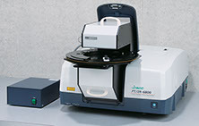
佳士科商贸有限公司为您提供《FTIR在材料和半导体领域研究和发展》,该方案主要用于其他中检测,参考标准--,《FTIR在材料和半导体领域研究和发展》用到的仪器有JASCO傅立叶变换红外光谱仪FT/IR-6000、JASCO FTIR-4000傅立叶变换红外光谱仪、jascoRFT-6000傅立叶变换红外拉曼光谱仪
推荐专场
相关方案
更多