


方案详情
文
长期以来阴极发光成像是地质研究的有力工具。最新的技术说明(technical note)为您讲解大面积高光谱阴极发光成像的采集模式。大面积(large area)光谱采集模式主要用于面积较大标本的阴极发光成像,例如锆石和其他矿物。
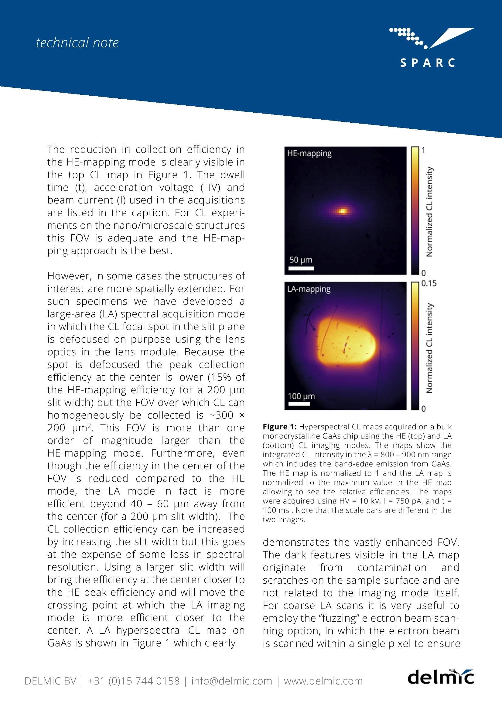
为了达到大面积阴极发光成像,特地调整光学模组中的光学器件,故意使狭缝平面中的CL焦点散焦。通过这一技术,我们就可以均匀地收集到较大阴极发光视场(FOV),视场大约~300×200μm2。通过调整狭缝宽度,平衡高效率(HE)和视野大小(与正常CL采集相比)
方案详情

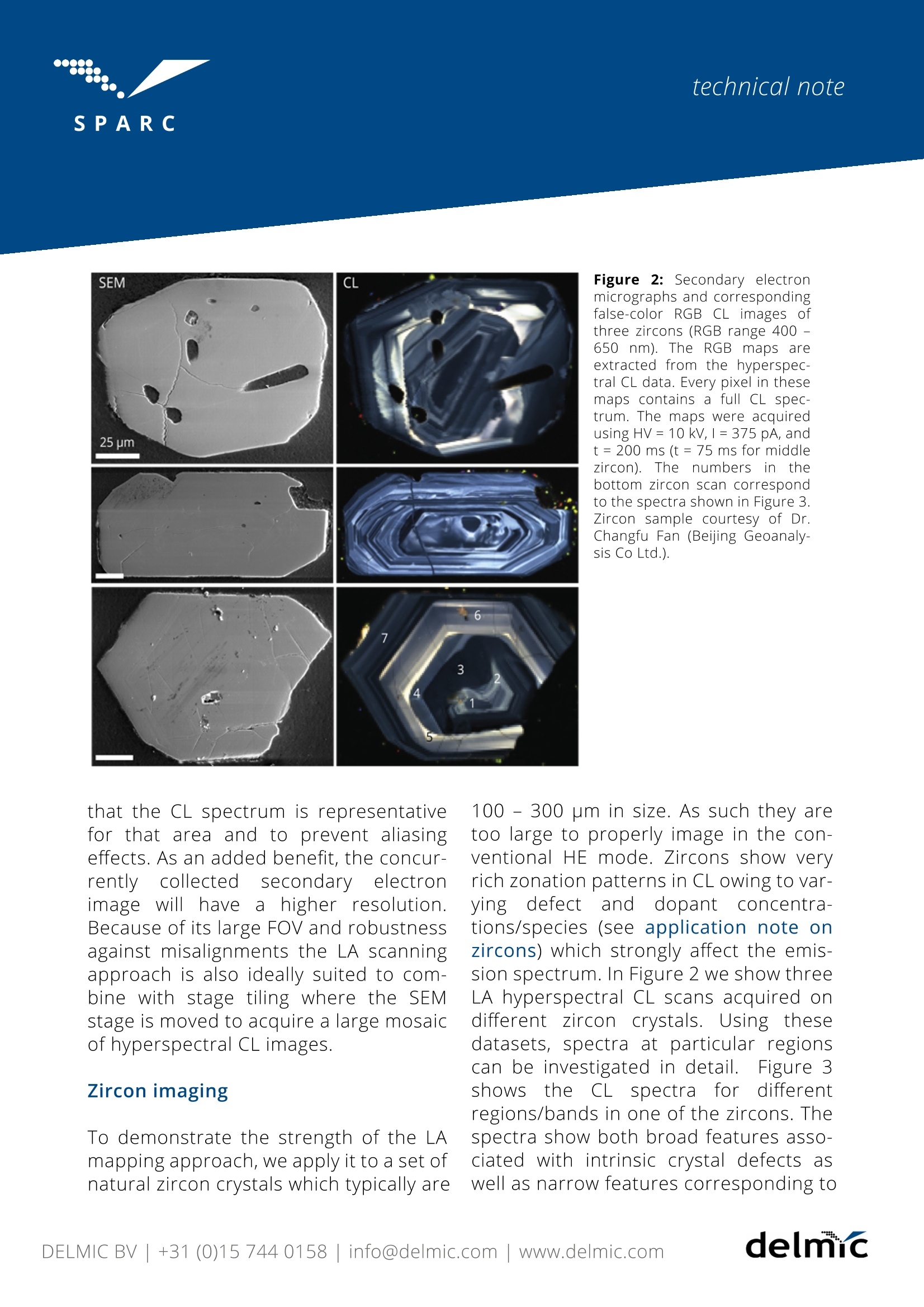
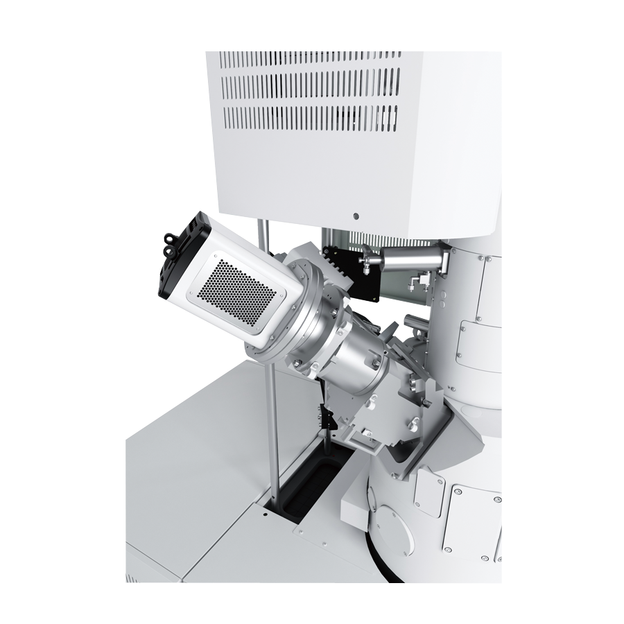
SPAR C technical note SPAR'C technical note Large-area hyperspectral cathodoluminescence imaging delnc In hyperspectral cathodoluminescenceimaging, the full emission spectrum isrecorded for a given electron beam posi-tion. In this imaging mode, light is senttowards a slit in a spectrograph (or anoptical fiber if an external spectrographISused),afterwhichthelight iisdispersed by a diffraction grating andthe spectrum is measured with a pixelat-ed CCD/CMOS camera (see technicalniote on hyperspectral imagingformore details) Large area CL imaging For efficient CL imaging the light has tobe focused onto the input slit such thatthe majority of CL is transmitted into thespectrograph,whichisachieved byproper alignment of theparaboloidcollection mirrorand focusinglensoptics. This high-efficiency(HE) collec-tion mode is conventionally used for CLexperiments in the SPARC as it providesthe ultimate performance in terms of signal to noise ratio. The paraboloidalignment is typically performed for acentral electron beam position within thefield of view (FOV) of the SEM. However,for many experiments CL image data isacquiredin1ia 2D raster scanwhichmeans that the electron beam has tomove with respect to this optimal focalposition. When the electron beam movesaway from the focal point of the parabo-loid the focal CL spot in the slit-planestarts to expand to the degree that it ispartially blocked by the slit. As a resultthe FOV from which CL can be homoge-neously extracted is limited to ~15×10um?,depending on the chosen slit width.The asymmetry in the FOV comes fromthe asymmetry in the paraboloid/slitgeometry, where the FOV along the opti-cal axis of the paraboloid is ~50% largercompared to the transverse direction.The FOV can be measured by acquiring aCL scan on ahomogenously emittingsample for which we use a single-crystalGaAs substrate in this case. The reduction in collection efficiency inthe HE-mapping mode is clearly visible inthe top CL map in Figure 1. The dwelltime (t), acceleration voltage(HV) andbeam current (l) used in the acquisitionsare listed in the caption. For CL experi-ments on the nano/microscale structuresthis FOV is adequate and the HE-map-ping approach is the best. However, in some cases the structures ofinterest are more spatially extended. Forsuch specimens we have developed alarge-area (LA) spectral acquisition modein which the CL focal spot in the slit planeis defocused on purpose using the lensoptics in the lens module. Because thespot is defocused the peak collectionefficiency at the center is lower (15% ofthe HE-mapping efficiency for a 200 pmslit width) but the FOV over which CL canhomogeneously be collected is ~300 x200 um2. This FOV is more than oneorder of magnitude larger thantheHE-mapping mode. Furthermore, eveenthough the efficiency in the center of theFOV is reduced compared to the HEmode, the LA mode in fact ismoreefficient beyond 40 - 60 um away fromthe center (for a 200 um slit width). TheCL collection efficiency can be increasedby increasing the slit width but this goesat the expense of some loss in spectralresolution. Using a larger slit width willbring the efficiency at the center closer tothe HE peak efficiency and will move thecrossing point at which the LA imagingmode iss more efficient closer to thecenter. A LA hyperspectral CL map onGaAs is shown in Figure 1 which clearly 0 Figure 1: Hyperspectral CL maps acquired on a bulkmonocrystalline GaAs chip using the HE (top) and LA(bottom) CL imaging modes. The maps show theintegrated CL intensity in the 入=800-900 nm rangewhich includes the band-edge emission from GaAs.The HE map is normalized to 1 and the LA map isnormalized to the maximum value in the HE mapallowing to see the relative efficiencies. The mapswere acquired using HV = 10 kV, 1= 750 pA, and t=100 ms . Note that the scale bars are different in thetwo images. demonstrates the vastly enhanced FOV.The dark features visible in the LA maporiginatetrom contamination andscratches on the sample surface and arenot related to the imaging mode itself.For coarse LA scans it is very useful toemploy the "fuzzing" electron beam scan-ning option, in which the electron beamis scanned within a single pixel to ensure Figure 2: Secondary electronmicrographs and correspondingfalse-color RGB CL images ofthree zircons (RGB range 400 -650 nm). The RGB maps areextracted from the hyperspec-tral CL data. Every pixel in thesemaps contains a full CL spec-trum. The maps were acquiredusing HV=10 kV,1= 375 pA, andt= 200 ms (t =75 ms for middlezircon).. Thennumbersinthebottom zircon scan correspondto the spectra shown in Figure 3.Zircon sample courtesy of Dr.Changfu Fan (Beijing Geoanaly-sis Co Ltd.). that the CL spectrum is representativefor that area and to prevent aliasingeffects. As an added benefit, the concur-rentlycollectedsecondaryelectronimage willhave a higher resolution.Because of its large FOV and robustnessagainst misalignments the LA scanningapproach is also ideally suited to com-bine with stage tiling where the SEMstage is moved to acquire a large mosaicof hyperspectral CL images. Zircon imaging To demonstrate the strength of the LAmapping approach, we apply it to a set ofnatural zircon crystals which typically are 100 - 300 um in size. As such they aretoo large to properly image in the con-ventional HE mode. Zircons show veryrich zonation patterns in CL owing to var-ying defect anddopant conce ra-tions/species (see application note onzircons) which strongly affect the emis-sion spectrum. In Figure 2 we show threeLA hyperspectral CL scans acquired onint zircon ccrryyststalasl.s. Usingthesedatasets, spectra at particular regionscan be investigated in detail. FFigure 3showsthe CL spectra for differentregions/bands in one of the zircons. Thespectra show both broad features asso-ciatedwith intrinsic crystal defects aswell as narrow features corresponding to Figure 3: On the left CL spectraare shown for different electronbeam positions (see Figure 2).The spectra are normalized andoffset vertically for visibility.Onthe right we show the spectrumfor position 6 in more detail.The sharp peaks present in thespectrum can be attributed toparticular rare-earthelementspecies as indicated. the emission of rare-earth elements. Thelatter can be identified based on the peakpositions(seeapplicationnote onrare-earth dopedmaterialsffor moredetails). The small bright yellow and redcolored particles visible at the edge ofthe zircons in some places correspond toresidual diamond particles from the pol-ishing process. Applicability of the technique The LA imaging is available for everySPARC spectral system and can be usedfor both detector slots on the integratedspectrometer. For a fiber-coupled spec-trograph the efficiency of the LA mode ismore limited as the fiber input facet actsas a 2D spatial filter leading to a largerloss in intensity compared to the slitwhich only acts as a 1D spatial filter. TheLA technique works particularly well onflat (polished) substrates. In samples withstrong surface topography or nanostruc-turing shadowing effects and/or distorted spectra if the LA mode is used. To checkthe validity of the LA mapping techniqueon given sample there are severales: 1) Scar sanHE mode (albeit on a smaller area) andchecking that it gives similar results tothe LA mode. 2) Scanning the sample indifferent orientations with respect to theparaboloid mirror in LA mode and check-ing whether the results are similar. Thesample can be rotated with SEM stage forthis check. 3) Checking the degree ofdirectionality/shadowinginangle-re-solved cathodoluminescence imaging (ifavailable). If this is limited, the LA methodcan be applied without any distortions. DELMIC B.V. is a company based in Delft, the Netherlands thatproduces correlative light and electron microscopy solutions.DELMIC's systems cater to a broad range of researchers infields ranging from nanophotonics to cell biology. The SPARC is a high-performance cathodoluminescencedetection system produced by DELMIC. The system is designedto optimally collect and detect cathodoluminescence emission,enabling fast and sensitive material characterization at thenanoscale. For questions regarding this note, contact our SPARC ProductManager Toon Coenen at: coenen@delmic.com For more resources, see: www.delmic.com/resources For more information on the SPARC, visit: www.delmic.com/sparc delnc delmic.com The Netherlands delmcDELMIC BV+()nfo@delmic.com www.delmic.com 长期以来阴极发光成像是地质研究的有力工具。最新的技术说明(technical note)为您讲解大面积高光谱阴极发光成像的采集模式。大面积(large area)光谱采集模式主要用于面积较大标本的阴极发光成像,例如锆石和其他矿物。 为了达到大面积阴极发光成像,我们特地调整光学模组中的光学器件,故意使狭缝平面中的CL焦点散焦。通过这一技术,我们就可以均匀地收集到较大阴极发光视场(FOV),视场大约~300×200μm2。通过调整狭缝宽度,平衡高效率(HE)和视野大小(与正常CL采集相比)。该技术说明(technical note)展示了以锆石晶体为例的大面积映射方法的优势。对于传统的高光谱阴极发光成像来说,通常尺寸为100-300μm的锆石面积过大。但通过以上大面积高光谱阴极发光扫描,就可以在特定区域观察和研究光谱细节。高光谱位于微区分析非常有意义,可以揭示如与固有晶体缺陷和稀土元素发射相关的细节特征。文章详情,请点击“阅读原文”或链接http://www.dervee.com/uppic/20190329/20190329152103663066.pdfCathodoluminescence imaging is a powerful tool for acquiring data from geological samples. Our new technical note describes in detail an acquisition mode called large-area hyperspectral cathodoluminescence imaging. Large-area (LA) spectral acquisition mode can be specifically used for imaging spatially extended specimen such as zircons and other minerals.In order to perform this cathodoluminescence imaging technique, the CL focal spot in the slit plane has to be defocused on purpose, using the lens optics in the lens module. The field of view (FOV) over which cathodoluminescence can homogeneously be collected is ~300 × 200 μm2. By adjusting the slid width it is possible to achieve both high-efficiency (HE) and the vastly enhanced field of view (compared to normal CL acquisition). The technical note demonstrates the strength of LA mapping approach on the example of zircon crystals. Being typically 100-300 μm in size, these minerals are normally too large for a conventional hyperspectral cathodoluminescence imaging. By acquiring LA hyperspectral CL scans it is possible to observe and study in detail spectra at particular regions. The spectra can reveal, for example, features associated with intrinsic crystal defect and the emission of rare-earth elements. http://www.dervee.com/uppic/20190329/20190329152103663066.pdf
确定

还剩4页未读,是否继续阅读?

产品配置单
苏州德尓微仪器有限公司为您提供《锆石中地质稀有元素检测方案(电镜部件)》,该方案主要用于金属矿产中地质稀有元素检测,参考标准--,《锆石中地质稀有元素检测方案(电镜部件)》用到的仪器有SPARC -高性能SEM阴极发光成像系统
推荐专场
相关方案
更多