


方案详情
文
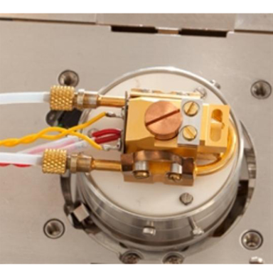
充分利用SEM的高空间分辨率, 结合阴极发光对材料的官能表征, 实现纳米级光学性能和材料结构表征。
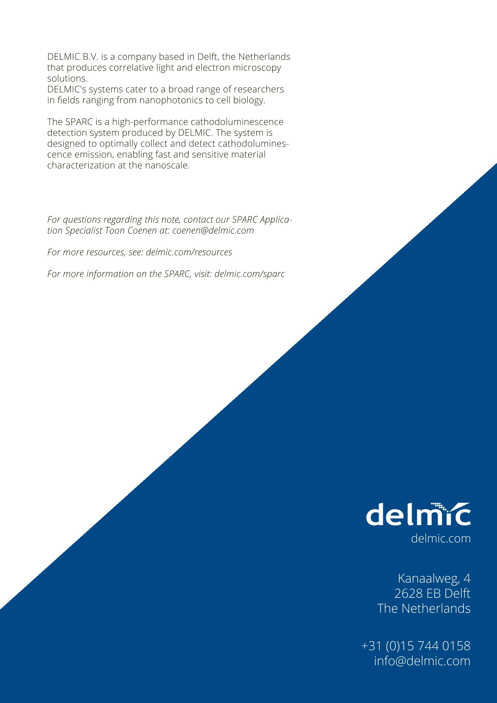
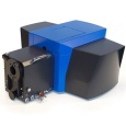
ARC(angle resolved cathodoluminescence)由FOM Institute of AMOLF的Albert Polman group 创新研发, 获得2014年MRS创新大奖。 后由荷兰Delmic公司重新设计并商用,它是一套高性能的阴极荧光检测系统。凭借独特的高精度镜面,SPARC开辟了新的研究途径,如电子束引起的纳米光子学。灵敏度和易用性,SPARC帮助科学家推动阴极荧光到更多和更高阶应用。
方案详情

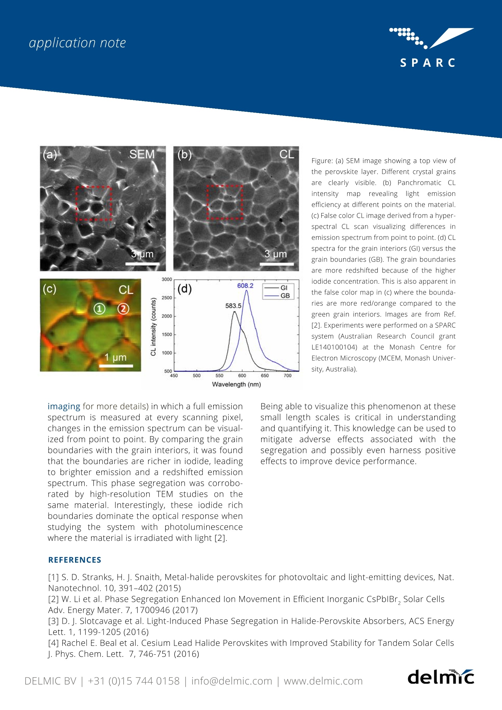
application noteSPARC SPAR'C application note Cathodoluminescence imaging on perovskites: phase segregation in inorganic CsPblBr2 delnc Image courtesy of Dr. Wei Li (Department ofMaterials Science and Engineering, MonashUniversity, Melbourne) Perovskite materials have gained significant inter-est because of their potential for cheap, flexible,and efficient optoelectronic devices such as solarcells and light-emitting diodes [1]. Perovskite is acollective term for materials that have an ABXcomposition and a perovskite crystal structure.Here, A can either be an organic cation such asCHNH*(methylammonium, MA*), H,NCHNH,+(formamidinum, FA*), or an inorganic cation suchas Cst. B is a metal dication such as Ge2+, Pb2+, orSn2+and Xis a halogen anion such as Cl, Br,orl. In this note, we focus on CsPbIBr,, a fully inorgan-ic perovskite material in which a mix of iodide andbromide is present [2]. Using a mixed halide com-position it is possible to boost power conversionefficiencies. However, it is known that under theinfluence of external stimuli such as light the IandBr halogen ions canmovewithin theperovskite material leading to phase segregation.Such segregation can have a major impact on theelectrical properties of the material and its func-tion as a solar cell or light emitting device [3,4]. which means that high-resolution microscopytechniques have to be used to investigate it.Cathodoluminescence (CL)microscopyISanexcellent tool in this context. Generally, CLmicroscopy allows studying the optical/materialproperties of semiconductors by mapping the CLemission at subwavelength length scales. Indirect band gapsemiconductors suchasperovskites the CL emission normally is dominat-ed by band edge emission, although defect emis-sion can also be visible depending on the (qualityof the) material. The Cs based material is morerobust than partially organic perovskite materi-als, which makes it more suitable for microscopicoptical and electron beam studies. As such itserves as a good model system for perovskitematerials in general. Figure:(a) SEM image showing a top view ofthe perovskite layer. Different crystal grainsare (clearlyvisible. (b)Panchromatic CLintensityy map revealing lighntt emissionefficiency at different points on the material.(c) False color CL image derived from a hyper-spectral CL scan visualizing differences inemission spectrum from point to point. (d) CLspectra for the grain interiors (GI) versus thegrain boundaries (GB). The grain boundariesare more redshifted because of the higheriodide concentration. This is also apparent inthe false color map in (c) where the bounda-ries are more red/orange compared to thegreen grain interiors. Images are from Ref.[2]. Experiments were performed on a SPARCsystem (Australian Research Council grantLE140100104) at the Monash Centre forElectron Microscopy(MCEM, Monash Univer-sity,Australia). imaging for more details) in which a full emissionspectrum is measured at every scanning pixel,changes in the emission spectrum can be visual-ized from point to point. By comparing the grainboundaries with the grain interiors, it was foundthat the boundaries are richer in iodide, leadingto brighter emission and a redshifted emissionspectrum. This phase segregation was corrobo-ratedby high-resolution TEM studies on thesame material. Interestingly, these iodide richboundaries dominate the optical response whenstudying the system with photoluminescencewhere the material is irradiated with light [2]. Being able to visualize this phenomenon at thesesmall length scales is critical in understandingand quantifying it. This knowledge can be used tomitigate adverse effects associated with thesegregation and possibly even harness positiveeffects to improve device performance. REFERENCES [1] S. D. Stranks,H.J. Snaith, Metal-halide perovskites for photovoltaic and light-emitting devices, Nat.Nanotechnol. 10, 391-402(2015) [2] W. Li et al. Phase Segregation Enhanced Ion Movement in Efficient Inorganic CsPblBr, Solar CellsAdv. Energy Mater. 7, 1700946 (2017) [3] D.J. Slotcavage et al. Light-Induced Phase Segregation in Halide-Perovskite Absorbers, ACS EnergyLett.1,1199-1205(2016) [4] Rachel E. Beal et al. Cesium Lead Halide Perovskites with Improved Stability for Tandem Solar CellsJ. Phys. Chem. Lett. 7, 746-751 (2016) DELMIC B.V. is a company based in Delft, the Netherlandsthat produces correlative light and electron microscopysolutions. DELMIC's systems cater to a broad range of researchersin fields ranging from nanophotonics to cell biology. The SPARC is a high-performance cathodoluminescencedetection system produced by DELMIC. The system isdesigned to optimally collect and detect cathodolumines-cence emission, enabling fast and sensitive materialcharacterization at the nanoscale. For questions regarding this note, contact our SPARC Applica-tion Specialist Toon Coenen at: coenen@delmic.com For more resources, see: delmic.com/resources For more information on the SPARC, visit: delmic.com/sparc delmic delmic.com Kanaalweg, 4 The Netherlands delmicDELMIC BV I+nfo@delmic.com www.delmic.com Cathodoluminescence imaging on perovskites: phase segregation in inorganic CsPbIBr2In this note, we focus on CsPbIBr2, a fully inorgan- ic perovskite material in which a mix of iodide and bromide is present [2]. Using a mixed halide com- position it is possible to boost power conversion efficiencies. However, it is known that under the influence of external stimuli such as light the I and Br halogen ions can move within the perovskite material leading to phase segregation. Such segregation can have a major impact on the electrical properties of the material and its func- tion as a solar cell or light emitting device [3,4].
确定
还剩2页未读,是否继续阅读?

产品配置单
苏州德尓微仪器有限公司为您提供《钙钛矿中晶体结构检测方案(电镜部件)》,该方案主要用于金属矿产中晶体结构检测,参考标准--,《钙钛矿中晶体结构检测方案(电镜部件)》用到的仪器有SPARC -高性能SEM阴极发光成像系统
推荐专场


相关方案
更多