


方案详情
文
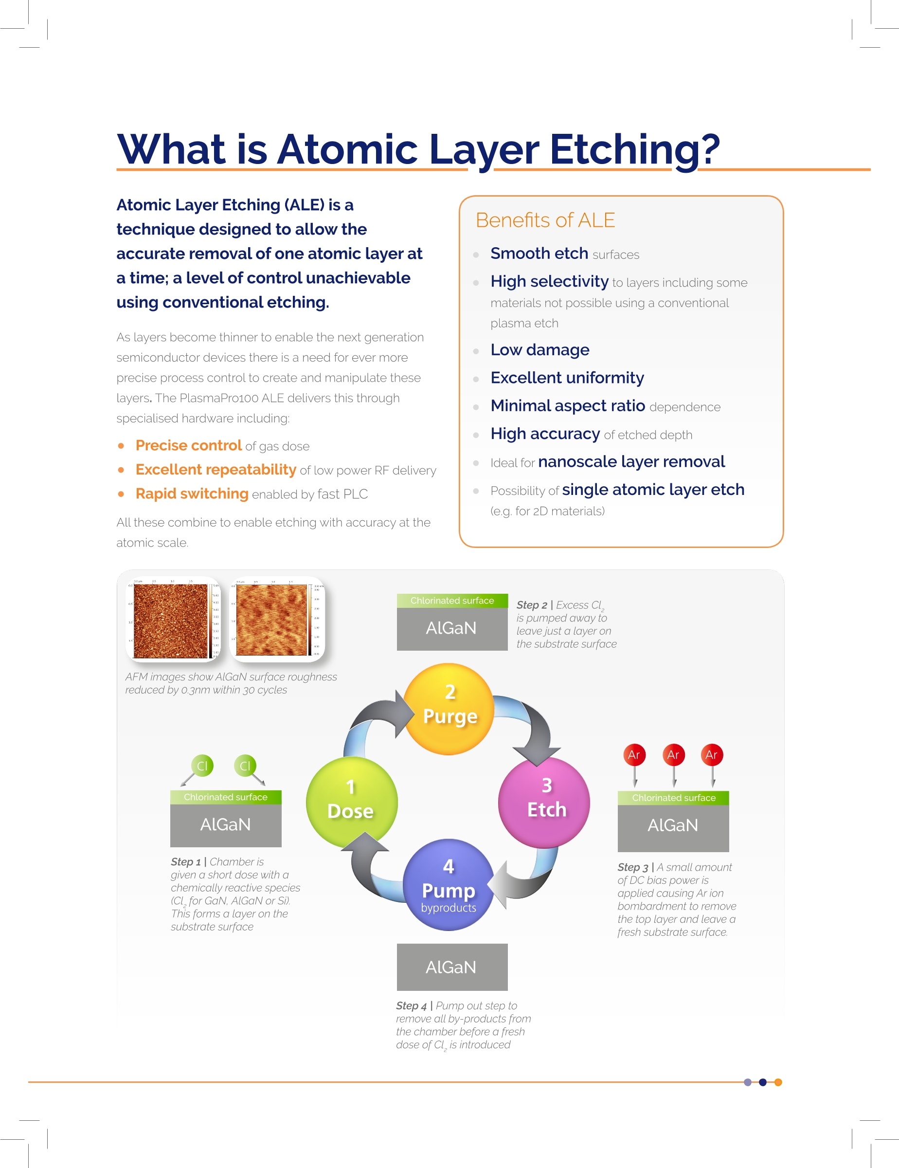
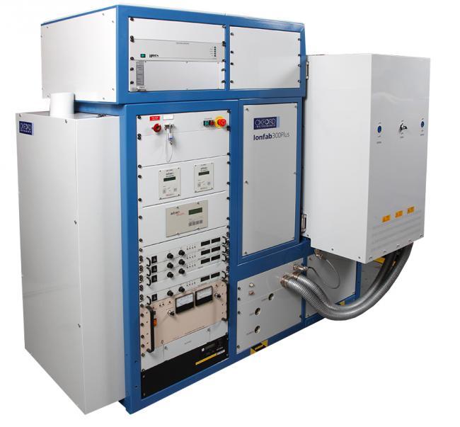
提供等离子体原子层刻蚀实现无损伤刻蚀。原子层蚀刻(ALE)是一种技术允许每次精确除去一个原子层,是使用常规刻蚀无法达到的控制水平。 牛津仪器的设备和工艺已通过充分验证,正常运转时间可达90%以上,一旦设备安装完毕,可立即投入使用。PlasmaPro 100系列市场应用广,包括但不限于: MEMS和传感器、光电子、分立元器件和纳米技术。它具有足够的灵活性,可用于研究和开发,通过打造质量满足生产需求。
方案详情

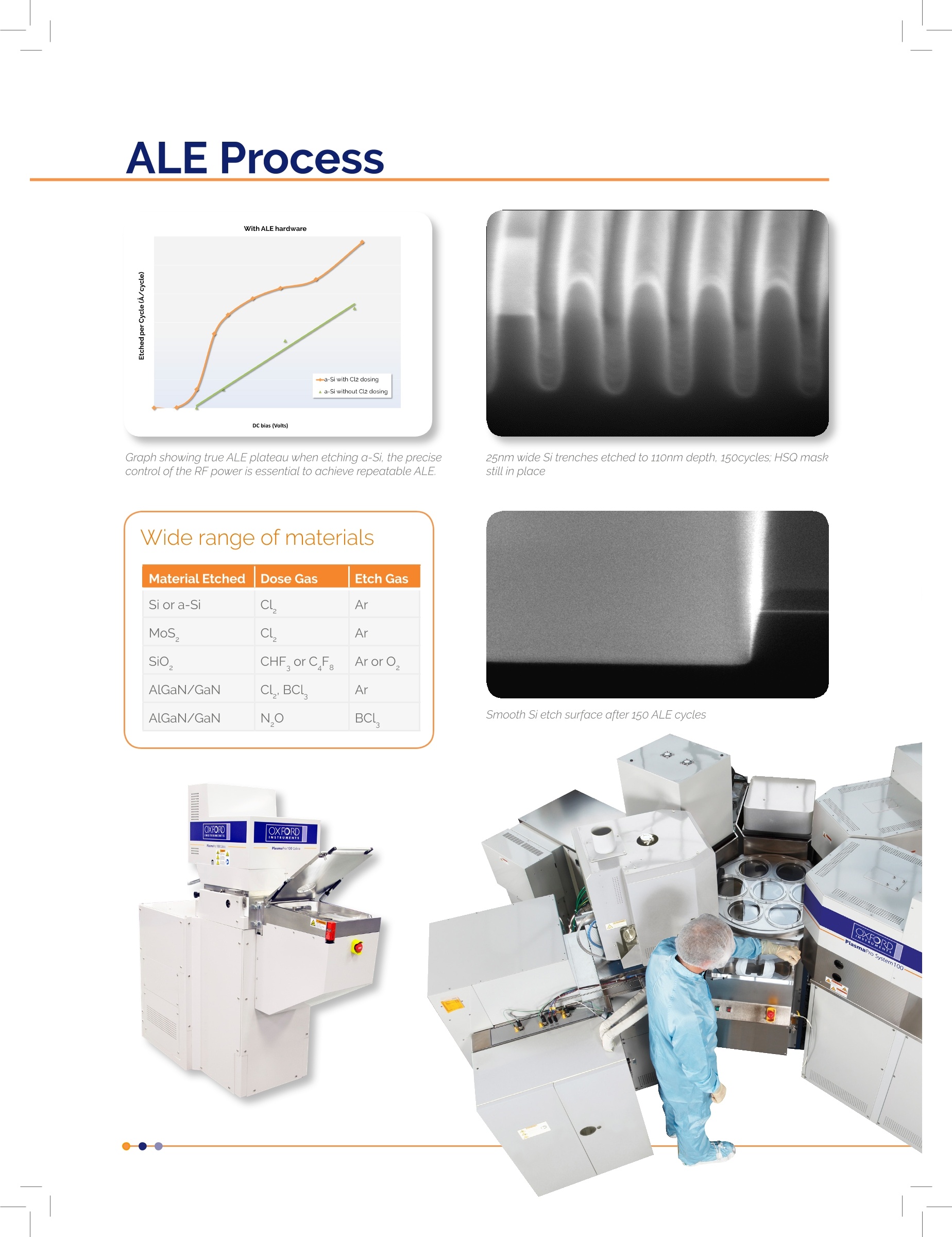
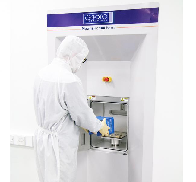
Atomic Layer Etching Innovative solutions for etching to the atomic layer Atomic Layer Etching (ALE) is atechnique designed to allow theaccurate removal of one atomic layer ata time; a level of control unachievableusing conventional etching. As layers become thinner to enable the next generationsemiconductor devices there is a need for ever moreprecise process control to create and manipulate theselayers. The PlasmaPro100 ALE delivers this throughspecialised hardware including: ●Precise control of gas dose Excellent repeatability of low power RF delivery Rapid switching enabled by fast PLC All these combine to enable etching with accuracy at theatomic scale. Benefits of ALEeSmooth etch surfacesHigh selectivity to layers including somematerials not possible using a conventionalplasma etchLow damageExcellent uniformityMinimal aspect ratio dependenceHigh accuracy of etched depthldeal for nanoscale layer removal●Possibility of single atomic layer etch(e.g. for 2D materials) ALE Process Graph showing true ALE plateau when etching a-Si, the precisecontrol of the RFpower is essential to achieve repeatable ALE 25nm wide Si trenches etched to 110nm depth, 150cycles; HSQ maskstill in place Smooth Si etch surface after 150 ALE cycles Global Serviceand Support Worldwide Service and Support For furtherinformation aboutour tools, pleasecontact your localOxford InstrumentsPlasma Technologyoffice Oxford Instruments is committed to supporting our customers' success.We recognise that this requires world class products complemented byworld class support. Our global service force is backed by regional offices,offering rapid support wherever you are in the world. For more information please emailplasmaaoxinst.com We can provide: UKYattonTel: +44 (0) 1934 837000 Flexible service agreements to meet your needs Germany TaiLored system training courses Wiesbaden Tel: +49 (0) 6122 937161 System upgrades and refurbishments India Immediate access to genuine spare partsand accessories Mumbai Tel: +91 22 4253 5100 JapanTokyoTel: +81 3 5245 3261 PR China Beijing Tel: +86 10 6518 8160/1/2 Shanghai Tel: +86 21 6132 9688 Singapore Tel:+65 6337 6848 Taiwan Tel:+886 3 5788696 US, Canada &Latin America Concord,MA TOLLFREE: +1 800 447 4717 visit plasma.oxinst.com for more information Oxford Instruments, at Yatton,UK. operates Quality Management Systems approved to therequirements of BS EN ISO 9001. This publication is the copyright of Oxford Instruments plc andprovides outline information only, which (unless agreed by the company in writing) may not beused, applied or reproduced for any purpose or form part of any order or contract or regarded asthe representation relating to the products or services concerned.Oxford Instruments policy is oneof continued improvement. The company reserves the right to alter without notice the specification,design or conditions of supply of any product or service, Oxford Instruments acknowledges alltrademarks and registrations. Certain processes are not offered in a few countries, respecting localpatents. O Oxford Instruments plc, 2018. AlL rights reserved.RefOIPT/ALE/2018/001 OXFORDINSTRUMENT S 原子层蚀刻(ALE)是一种技术允许每次精确除去一个原子层,是使用常规刻蚀无法达到的控制水平。 牛津仪器的设备和工艺已通过充分验证,正常运转时间可达90%以上,一旦设备安装完毕,可立即投入使用。PlasmaPro 100系列市场应用广,包括但不限于: MEMS和传感器、光电子、分立元器件和纳米技术。它具有足够的灵活性,可用于研究和开发,通过打造质量满足生产需求。
确定
还剩2页未读,是否继续阅读?

产品配置单
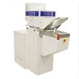
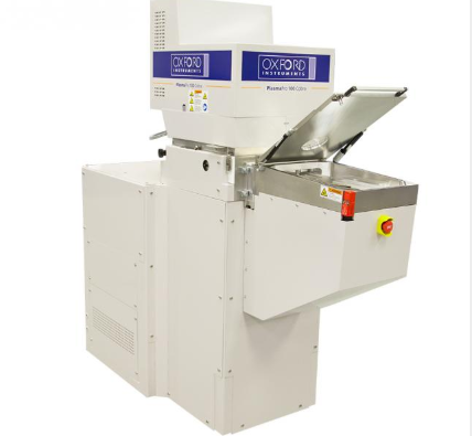
牛津仪器科技(上海)有限公司为您提供《等离子体中原子层蚀刻检测方案(半导体检测仪)》,该方案主要用于其他中原子层蚀刻检测,参考标准--,《等离子体中原子层蚀刻检测方案(半导体检测仪)》用到的仪器有牛津仪器PlasmaPro100 ALE原子层刻蚀
推荐专场
相关方案
更多