


方案详情
文
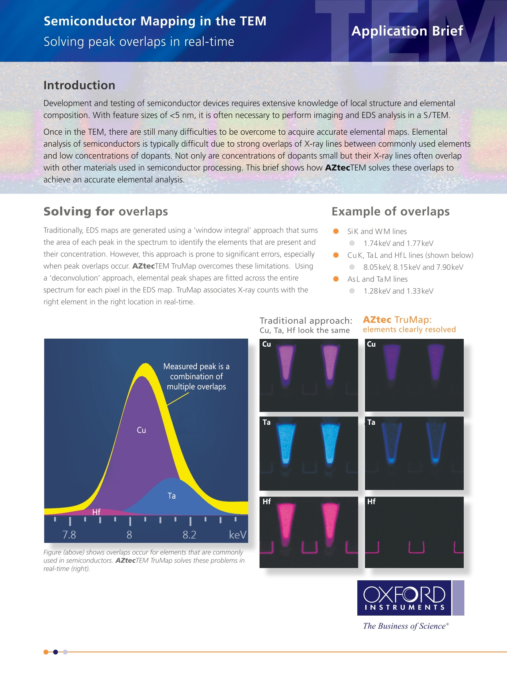
Development and testing of semiconductor devices requires extensive knowledge of local structure and elemental
composition. With feature sizes of <5 nm, it is often necessary to perform imaging and EDS analysis in a S / TEM.
Once in the TEM, there are still many difficulties to be overcome to acquire accurate elemental maps. Elemental
analysis of semiconductors is typically difficult due to strong overlaps of X-ray lines between commonly used elements
and low concentrations of dopants. Not only are concentrations of dopants small but their X-ray lines often overlap
with other materials used in semiconductor processing. This brief shows how AZtecTEM solves these overlaps to
achieve an accurate elemental analysis.
TEM Semiconductor Mapping in the TEM
Solving peak overlaps in real-time
Application Brief
方案详情

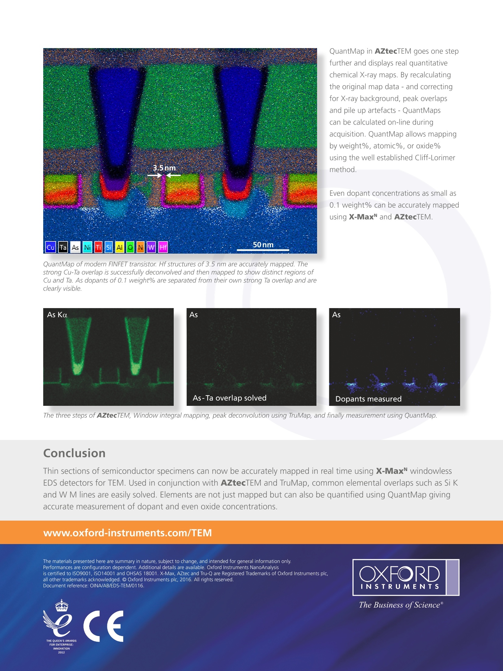
Semiconductor Mapping in the TEMSolving peak overlaps in real-time Application Brief Introduction Development and testing of semiconductor devices requires extensive knowledge of local structure and elementalcomposition. With feature sizes of <5 nm, it is often necessary to perform imaging and EDS analysis in a S/TEM. Once in the TEM,there are still many difficulties to be overcome to acquire accurate elemental maps. Elementalanalysis of semiconductors is typically difficult due to strong overlaps of X-ray lines between commonly used elementsand low concentrations of dopants. Not only are concentrations of dopants small but their X-ray lines often overlapwith other materials used in semiconductor processing. This brief shows how AZtecTEM solves these overlaps toachieve an accurate elemental analysis. Traditionally, EDS maps are generated using a 'window integral' approach that sumsthe area of each peak in the spectrum to identify the elements that are present andtheir concentration. However, this approach is prone to significant errors, especiallywhen peak overlaps occur. AZtecTEM TruMap overcomes these limitations. Usinga 'deconvolution' approach, elemental peak shapes are fitted across the entirespectrum for each pixel in the EDS map. TruMap associates X-ray counts with theright element in the right location in real-time. Example of overlaps SiK and WM lines ● 1.74keV and 1.77keV CuK, TaL and HfL lines (shown below) ● 8.05keV, 8.15keV and 7.90keV As L and Ta M lines ● 1.28keV and 1.33keV Traditional approach: AZtec TruMap:Cu, Ta, Hf look the same elements clearly resolved Figure (above) shows overlaps occur for elements that are commonlyused in semiconductors. AZtecTEM TruMap solves these problems inreal-time (right). INSTRUMENTS The Business of Science" QuantMap in AZtecTEM goes one stepfurther and displays real quantitativechemical X-ray maps. By recalculatingthe original map data - and correctingfor X-ray background, peak overlapsand pile up artefacts -QuantMapscan be calculated on-line duringacquisition. QuantMap allows mappingby weight%, atomic%, or oxide%using the well established Cliff-Lorimermethod. Even dopant concentrations as small as0.1 weight% can be accurately mappedusing X-Max" and AZtecTEM. QuantMap of modern FINFET transistor. Hf structures of 3.5 nm are accurately mapped. Thestrong Cu-Ta overlap is successfully deconvolved and then mapped to show distinct regions ofCu and Ta. As dopants of 0.1 weight% are separated from their own strong Ta overlap and areclearly visible. The three steps of AZtecTEM, Window integral mapping, peak deconvolution using TruMap, and finally measurement using QuantMap. Conclusion Thin sections of semiconductor specimens can now be accurately mapped in real time using X-Max windowlessEDS detectors for TEM. Used in conjunction with AZtecTEM and TruMap, common elemental overlaps such as Si Kand W M lines are easily solved. Elements are not just mapped but can also be quantified using QuantMap givingaccurate measurement ot dopant and even oxide concentrations. www.oxford-instruments.com/TEM The materials presented here are summary in nature, subject to change, and intended for general information only. Performances are configuration dependent. Additional details are available. Oxford Instruments NanoAnalysisis certified to ISO9001, ISO14001 and OHSAS 18001.X-Max, AZtec and Tru-Q are Registered Trademarks of Oxford Instruments plc,all other trademarks acknowledged. @ Oxford Instruments plc, 2016. All rights reserved. Document reference: OINA/AB/EDS-TEM/0116. The Business of Science" INNOVATION 2012 Development and testing of semiconductor devices requires extensive knowledge of local structure and elementalcomposition. With feature sizes of <5 nm, it is often necessary to perform imaging and EDS analysis in a S / TEM.Once in the TEM, there are still many difficulties to be overcome to acquire accurate elemental maps. Elementalanalysis of semiconductors is typically difficult due to strong overlaps of X-ray lines between commonly used elementsand low concentrations of dopants. Not only are concentrations of dopants small but their X-ray lines often overlapwith other materials used in semiconductor processing. This brief shows how AZtecTEM solves these overlaps toachieve an accurate elemental analysis.TEM Semiconductor Mapping in the TEMSolving peak overlaps in real-timeApplication Brief
确定
还剩1页未读,是否继续阅读?

产品配置单

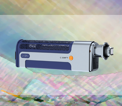
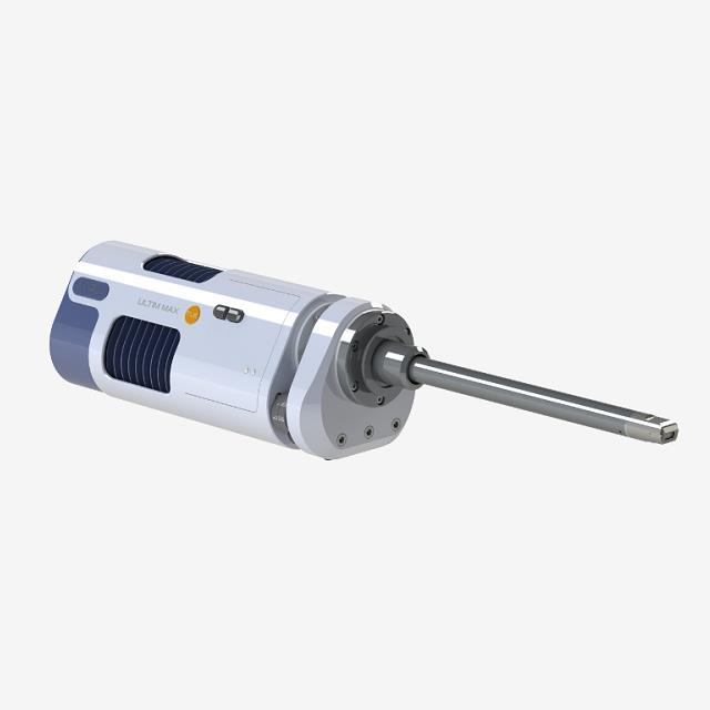
牛津仪器科技(上海)有限公司为您提供《半导体中局部结构和元素组成检测方案(EBSD系统)》,该方案主要用于其他中局部结构和元素组成检测,参考标准--,《半导体中局部结构和元素组成检测方案(EBSD系统)》用到的仪器有牛津仪器C-Swift EBSD探测器、电镜专用自动清洁度分析系统---牛津仪器AZtecFeature、电镜专用微区成分分析---牛津仪器Ultim Max能谱仪
推荐专场
电子背散射衍射系统(EBSD)
更多


相关方案
更多