


方案详情
文
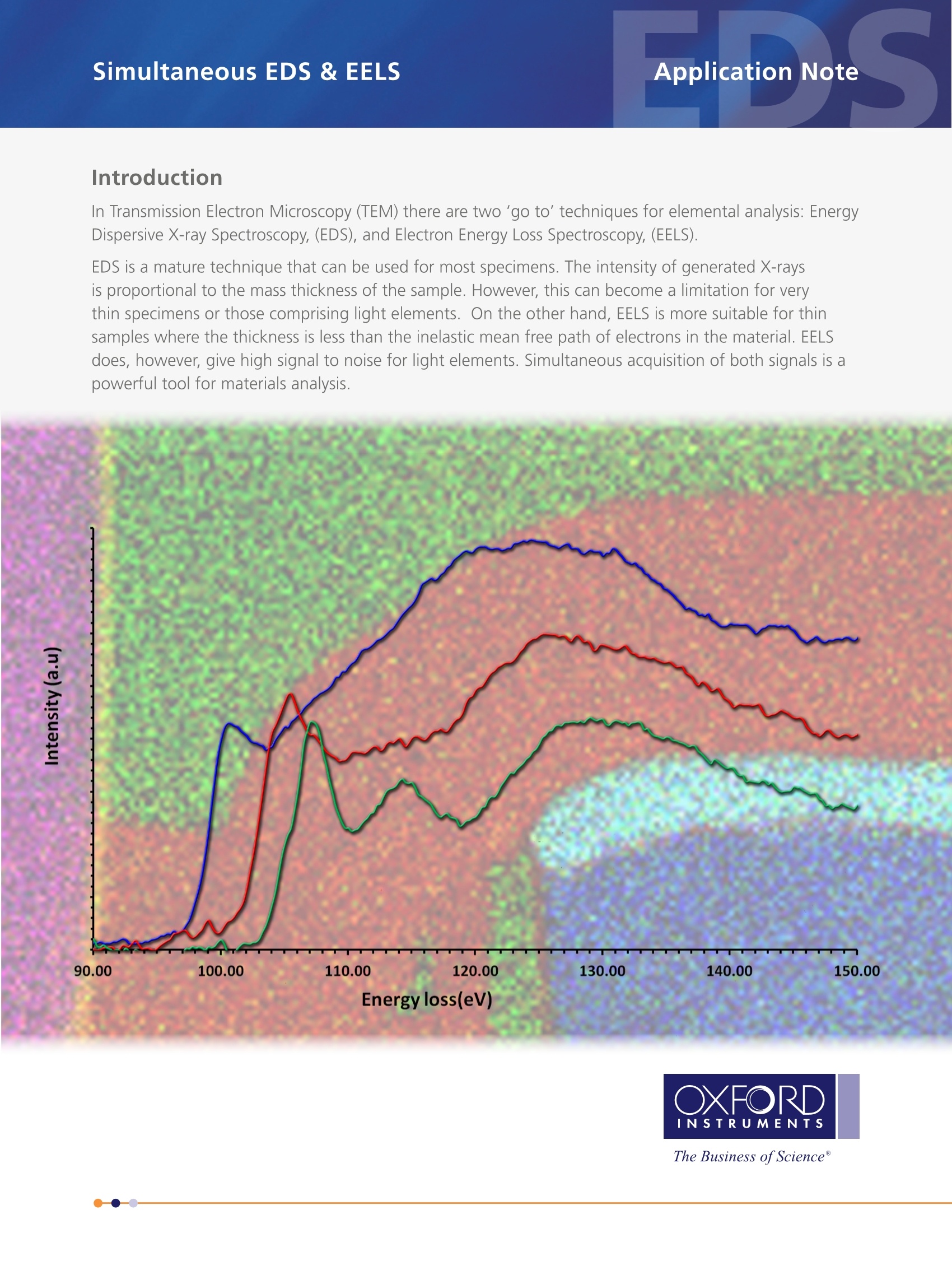
Introduction
In Transmission Electron Microscopy (TEM) there are two ‘go to’ techniques for elemental analysis: Energy
Dispersive X-ray Spectroscopy, (EDS), and Electron Energy Loss Spectroscopy, (EELS).
EDS is a mature technique that can be used for most specimens. The intensity of generated X-rays
is proportional to the mass thickness of the sample. However, this can become a limitation for very
thin specimens or those comprising light elements. On the other hand, EELS is more suitable for thin
samples where the thickness is less than the inelastic mean free path of electrons in the material. EELS
does, however, give high signal to noise for light elements. Simultaneous acquisition of both signals is a
powerful tool for materials analysis.
方案详情

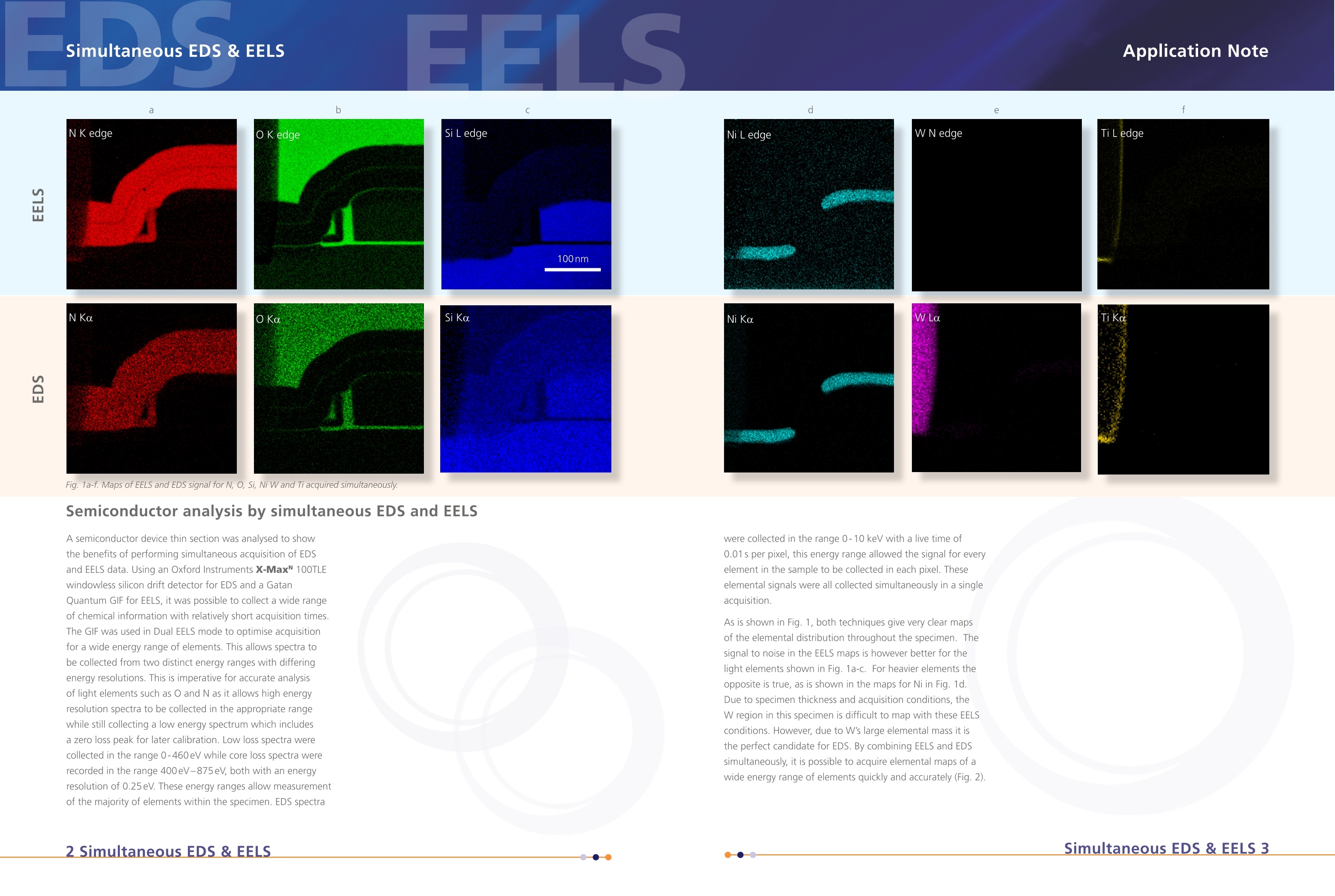
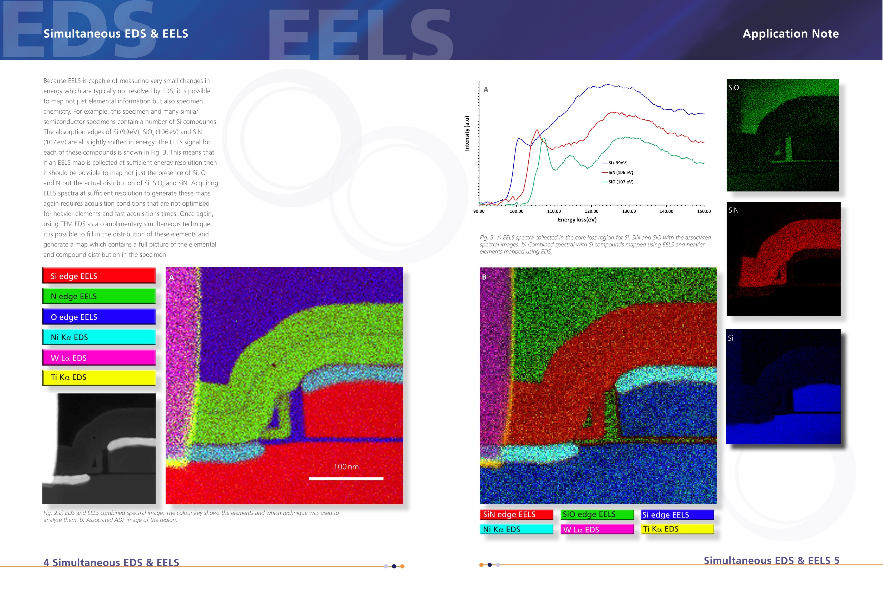
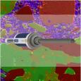
Application NoteSimultaneous EDS & EELS Introduction In Transmission Electron Microscopy (TEM) there are two 'go to'techniques for elemental analysis: EnergyDispersive X-ray Spectroscopy,(EDS), and Electron Energy Loss Spectroscopy, (EELS). EDS is a mature technique that can be used for most specimens. The intensity of generated X-raysis proportional to the mass thickness of the sample. However, this can become a limitation for verythin specimens or those comprising light elements. On the other hand, EELS is more suitable for thinsamples where the thickness is less than the inelastic mean free path of electrons in the material. EELSdoes, however, give high signal to noise for light elements. Simultaneous acquisition of both signals is apowerful tool for materials analysis. 90.00 100. 0 0 110.00 120.00 130.00 1 4 0.00 150.00 Energy loss(eV) The Business ofScience" FFLS ww TiLedge l Ni Ka sw Fig. 1a-f. Maps of EELS and EDS signal for N, O, Si, Ni W and Ti acquired simultaneously. Semiconductor analysis by simultaneous EDS and EELS A semiconductor device thin section was analysed to showthe benefits of performing simultaneous acquisition of EDSand EELS data. Using an Oxford Instruments X-Max100TLEwindowless silicon drift detector for EDS and a GatanQuantum GIF for EELS, it was possible to collect a wide rangeof chemical information with relatively short acquisition times.The GIF was used in Dual EELS mode to optimise acquisitionfor a wide energy range of elements. This allows spectra tobe collected from two distinct energy ranges with differingenergy resolutions. This is imperative for accurate analysisof light elements such as O and N as it allows high energyresolution spectra to be collected in the appropriate rangewhile still collecting a low energy spectrum which includesa zero loss peak for later calibration. Low loss spectra werecollected in the range 0-460 eV while core loss spectra wererecorded in the range 400eV-875eV both with an energyresolution of 0.25 eV. These energy ranges allow measurementof the majority of elements within the specimen. EDS spectra were collected in the range 0-10 keV with a live time of0.01 s per pixel, this energy range allowed the signal for everyelement in the sample to be collected in each pixel. Theseelemental signals were all collected simultaneously in a singleacquisition. As is shown in Fig. 1, both techniques give very clear mapsof the elemental distribution throughout the specimen. Thesignal to noise in the EELS maps is however better for thelight elements shown in Fig. 1a-c. For heavier elements theopposite is true, as is shown in the maps for Ni in Fig. 1d.Due to specimen thickness and acquisition conditions, theW region in this specimen is difficult to map with these EELSconditions. However, due to W's large elemental mass it isthe perfect candidate for EDS. By combining EELS and EDSsimultaneously, it is possible to acquire elemental maps of awide energy range of elements quickly and accurately (Fig. 2). Fig.2.a) EDS and EELS combined spectral image. The colour key shows the elements and which technique was used toanalyse them. b) Associated ADF image of the region. Fig.3. a) EELS spectra collected in the core loss region for Si, SiN and SiO with the associatedspectral images. b) Combined spectral with Si compounds mapped using EELS and heavierelements mapped using EDS. Conclusion The use of simultaneous EDS-EELS acquisition to fully characterise a semiconductor device specimen hasbeen demonstrated. It has been shown that, although each technique individually is able to characterisethe whole specimen, there are limitations to consider when optimising analysis. By using the EELSoptimised for light element analysis and the heavy element capabilities of EDS it is possible to generatefull specimen maps with improved signal to noise in shorter acquisition times. It was also shown that bycollecting EELS spectra at high energy resolution it is possible to identify not just single elements but alsocompounds. Using this technique the distributions of Si, SiN and SiO can be mapped in a specimen withhigh resolution while also using simultaneous EDS acquisition to map those elements not observable inthe chosen EELS energy range. Data collected in collaboration with the University of Warwick, UK. www.oxford-instruments.com/eds The Business of Science" Simy taneous EDS & EELSSimultaneous EDS & EELS Simy taneous EDS & EELS Simultaneous EDS & EELS IntroductionIn Transmission Electron Microscopy (TEM) there are two ‘go to’ techniques for elemental analysis: EnergyDispersive X-ray Spectroscopy, (EDS), and Electron Energy Loss Spectroscopy, (EELS).EDS is a mature technique that can be used for most specimens. The intensity of generated X-raysis proportional to the mass thickness of the sample. However, this can become a limitation for verythin specimens or those comprising light elements. On the other hand, EELS is more suitable for thinsamples where the thickness is less than the inelastic mean free path of electrons in the material. EELSdoes, however, give high signal to noise for light elements. Simultaneous acquisition of both signals is apowerful tool for materials analysis.
确定
还剩2页未读,是否继续阅读?

产品配置单
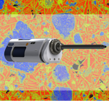
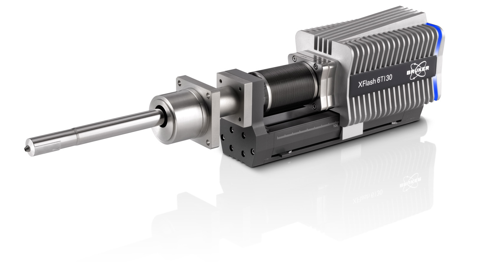
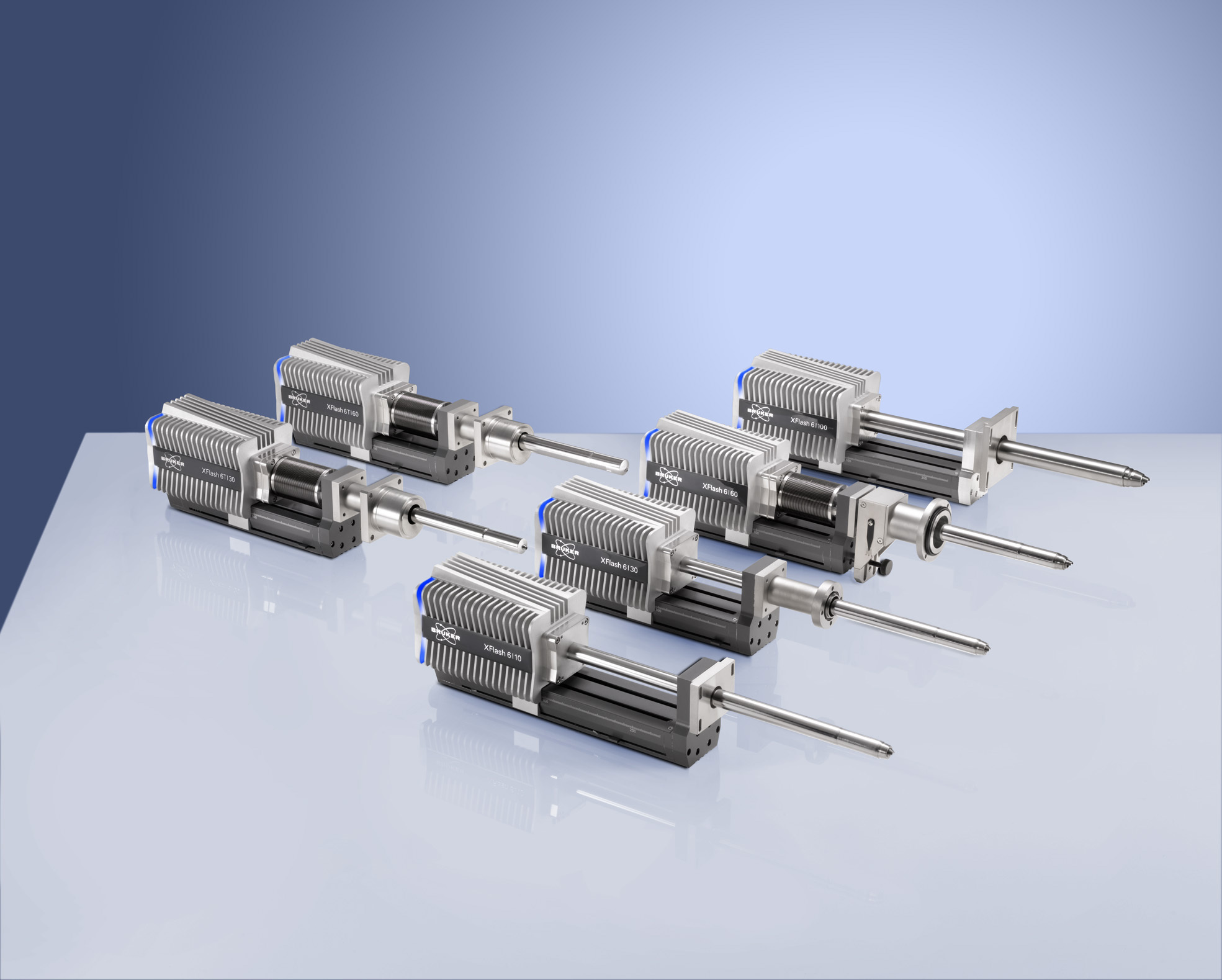
牛津仪器科技(上海)有限公司为您提供《半导体器件样品中完全表征检测方案(X射线能谱仪)》,该方案主要用于其他中完全表征检测,参考标准--,《半导体器件样品中完全表征检测方案(X射线能谱仪)》用到的仪器有电镜专用微区成分分析---牛津仪器Xplore能谱仪
推荐专场
相关方案
更多