


采用立陶宛Ekspla公司的T-Spec型太赫兹时域光谱仪,对可拉伸超薄碳聚合物双层在太赫兹波段的吸收特性进行了研究。表明这是一种理想的太赫兹吸收体,可以吸收99.9%以上的太赫兹波。
方案详情

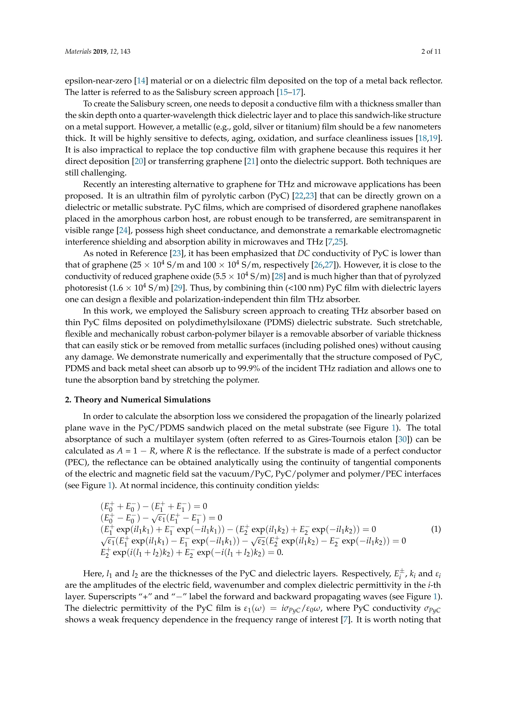
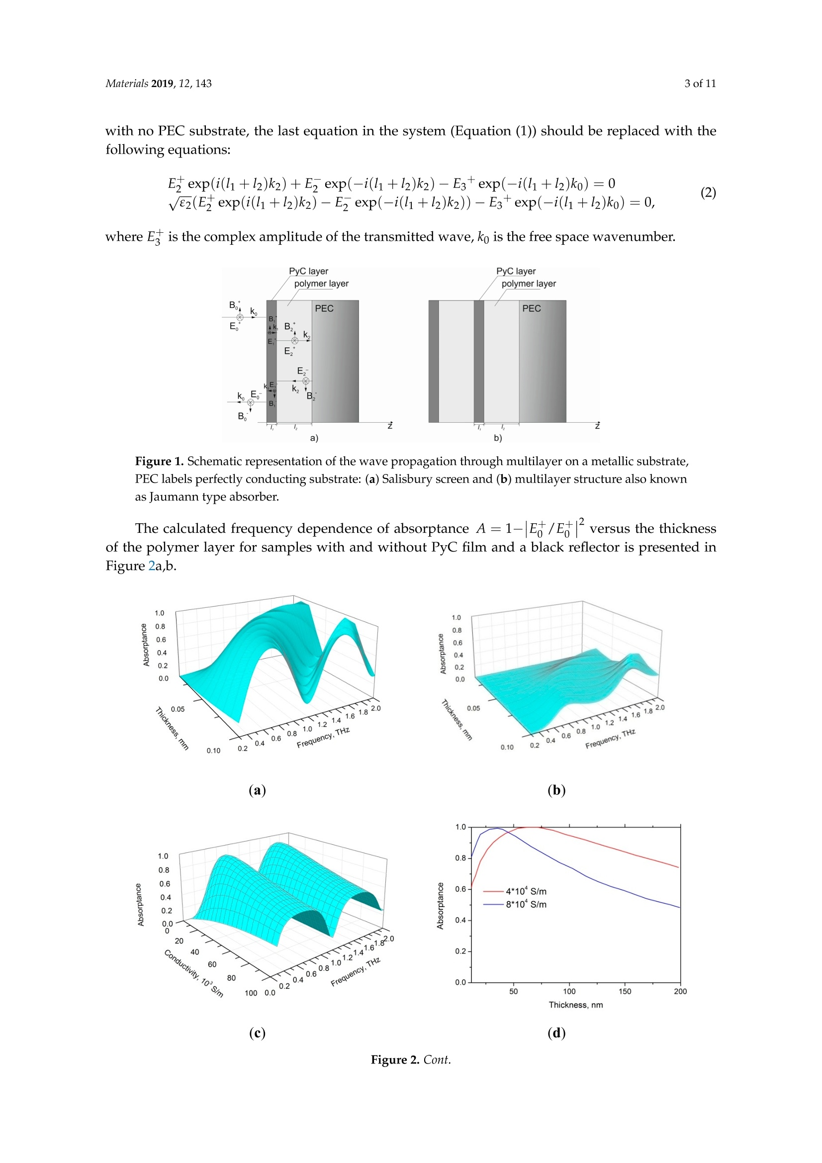
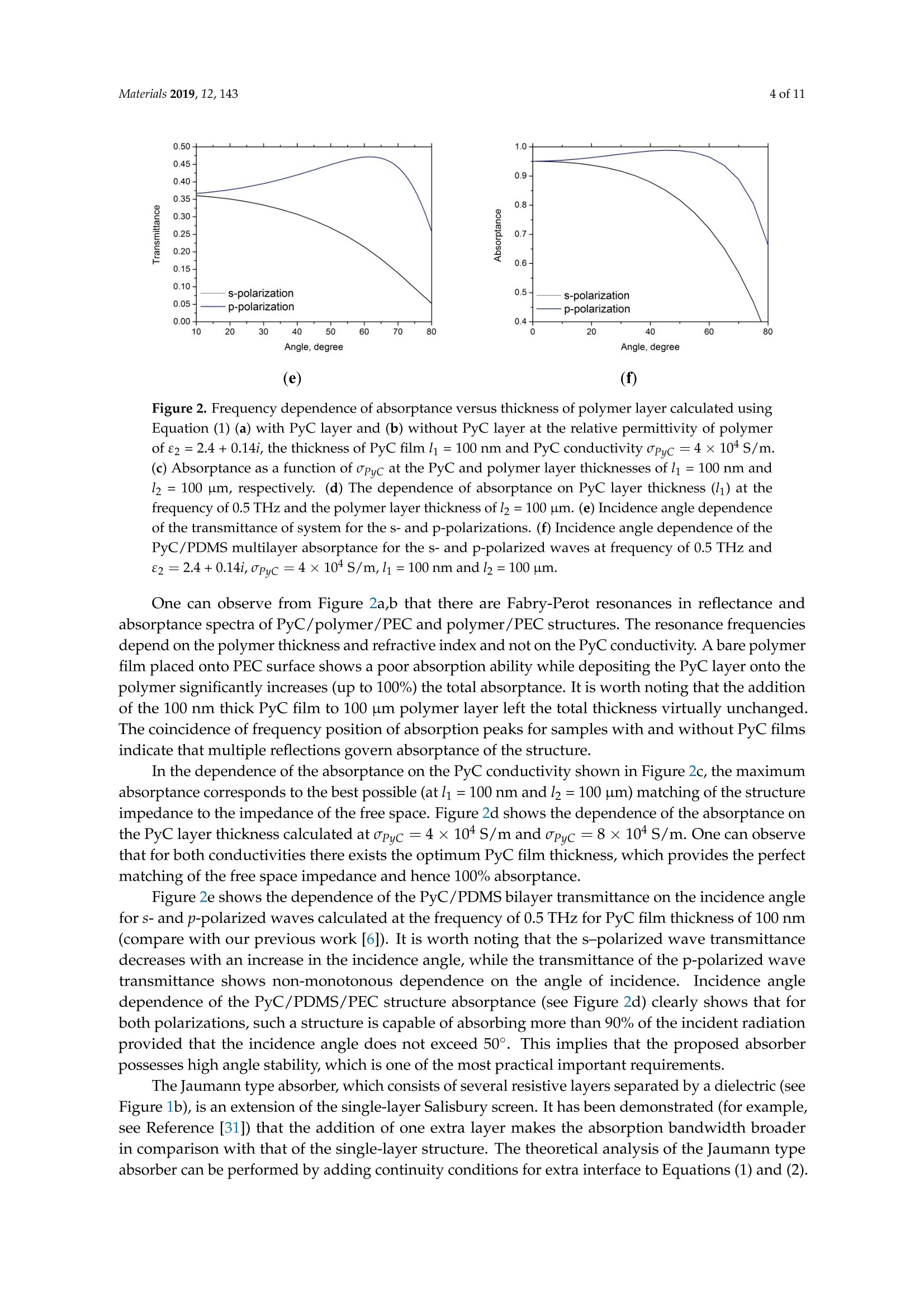
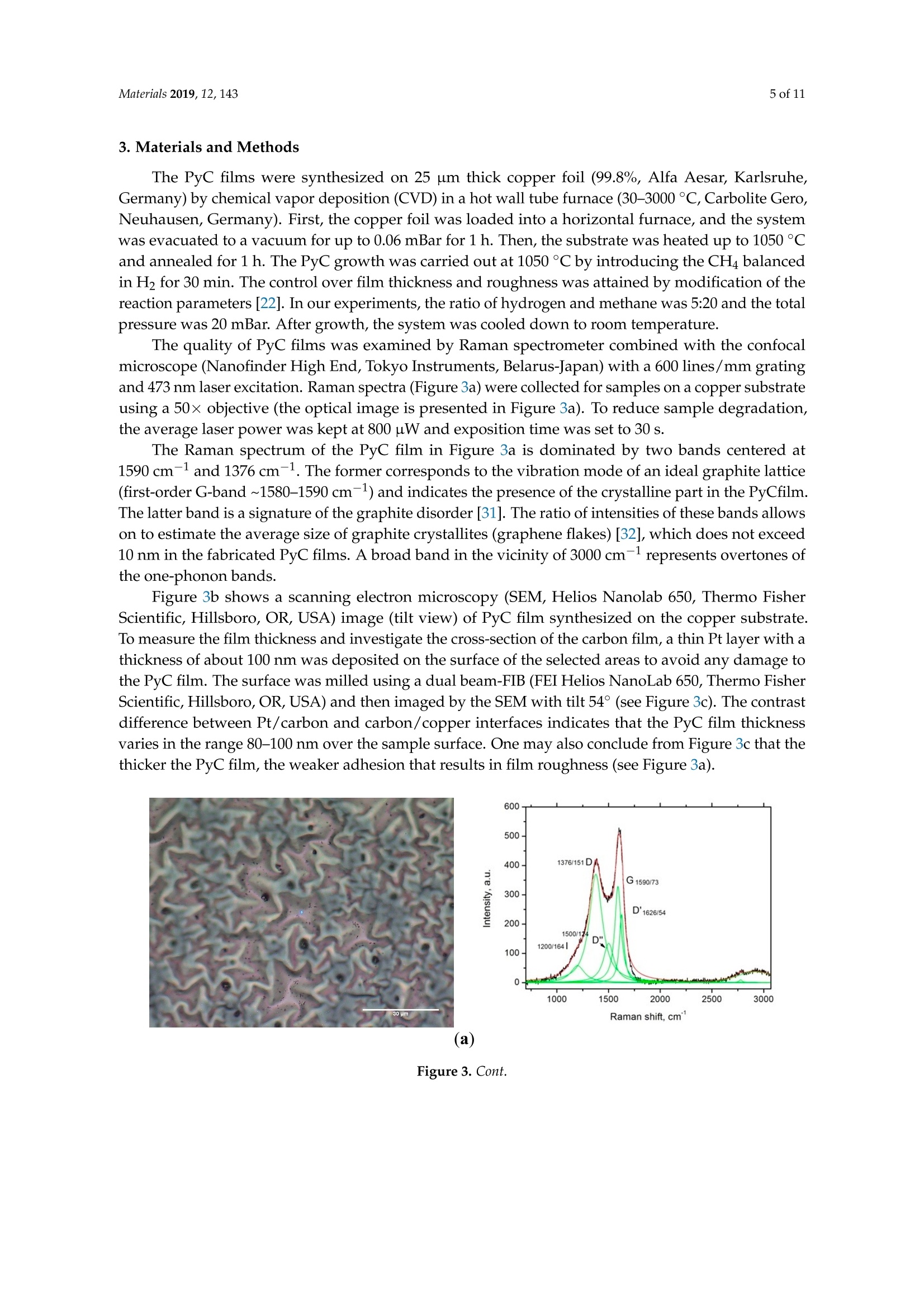
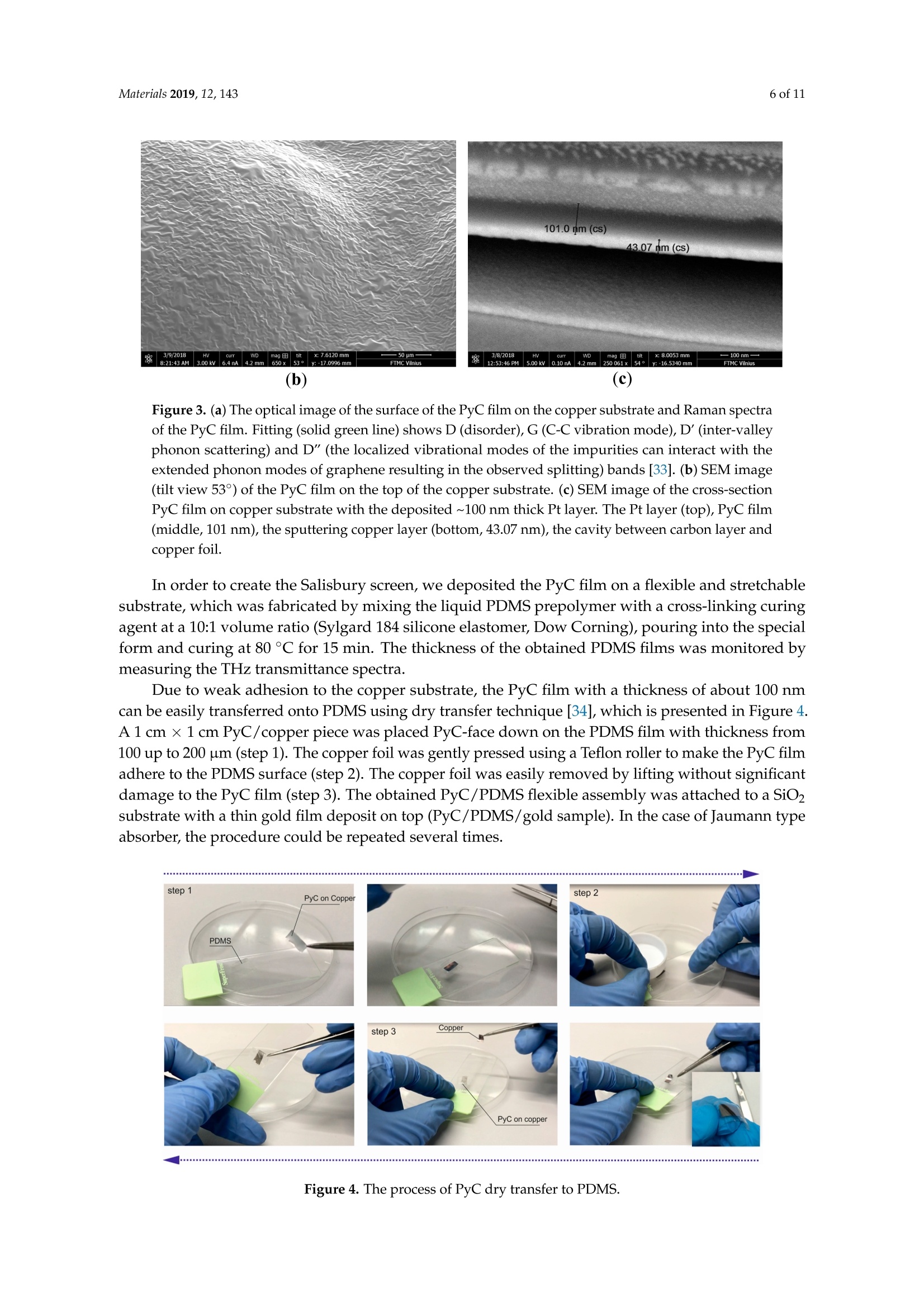
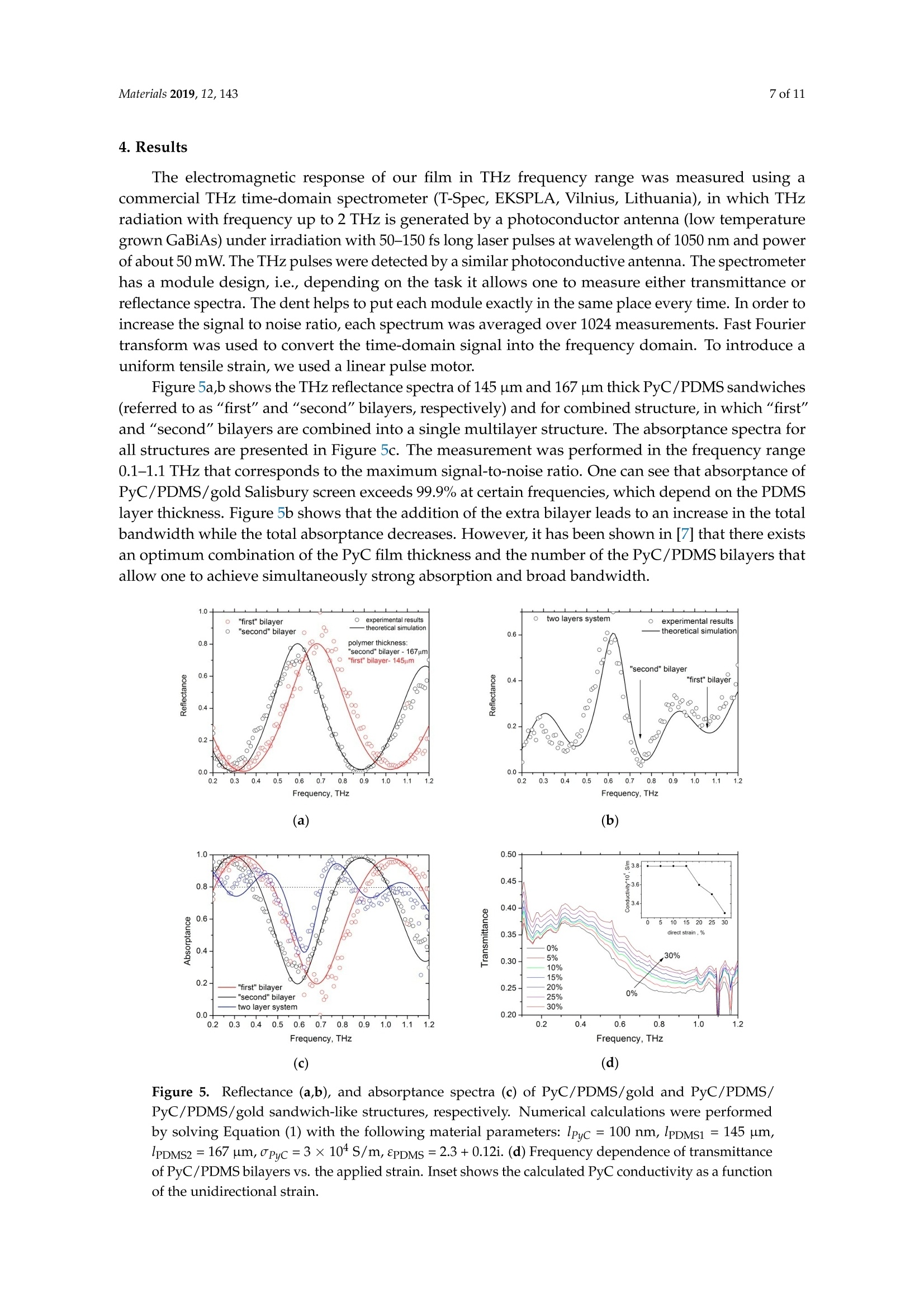
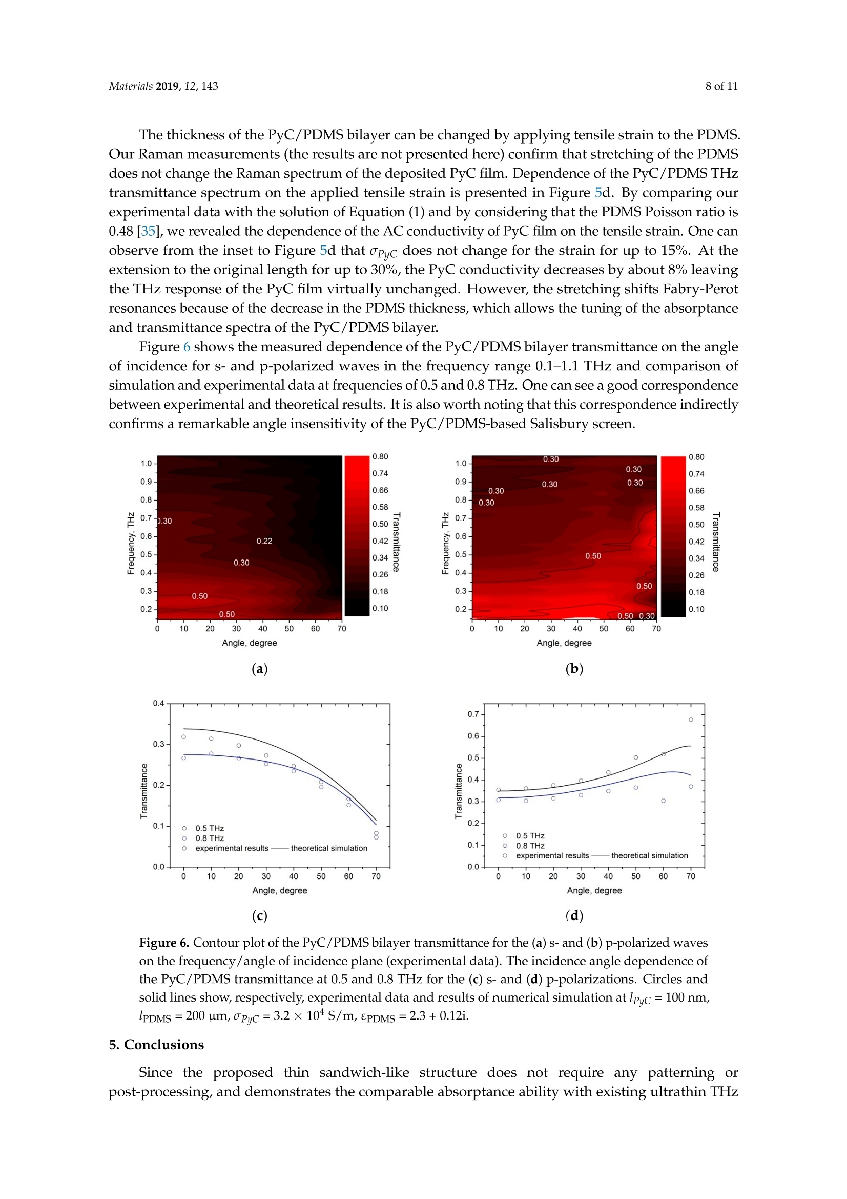
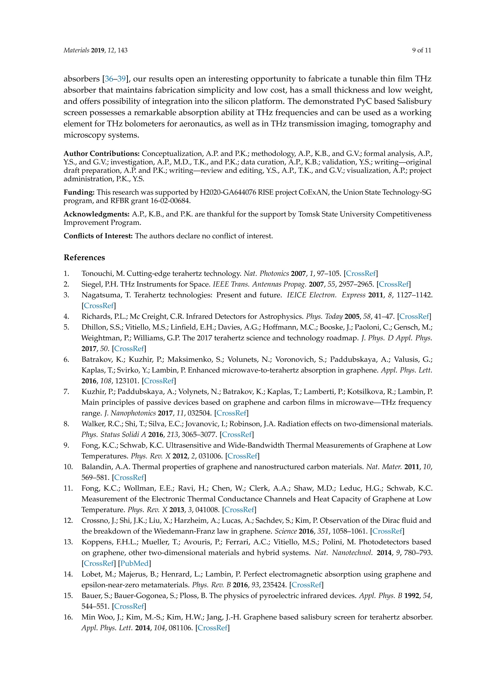
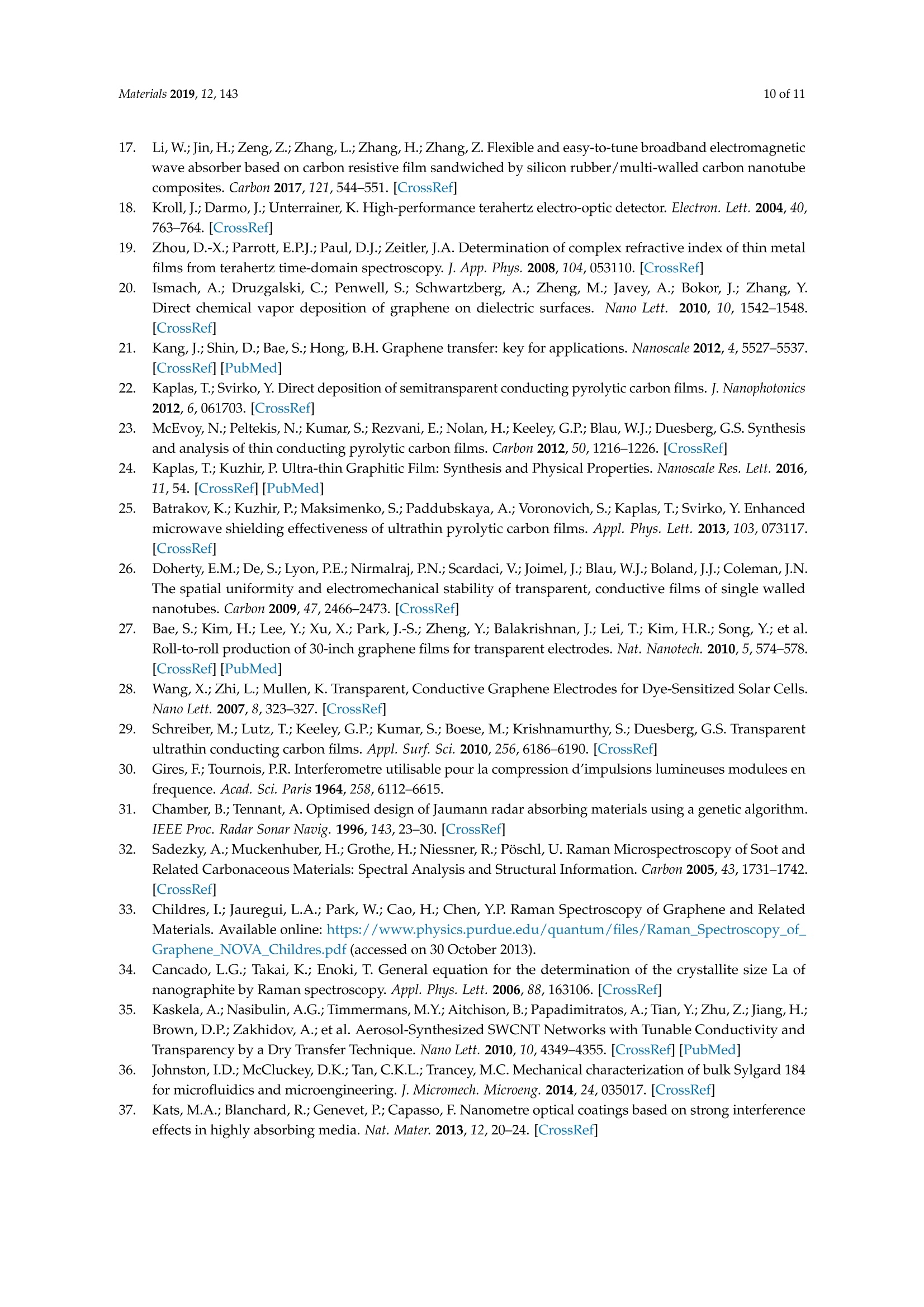
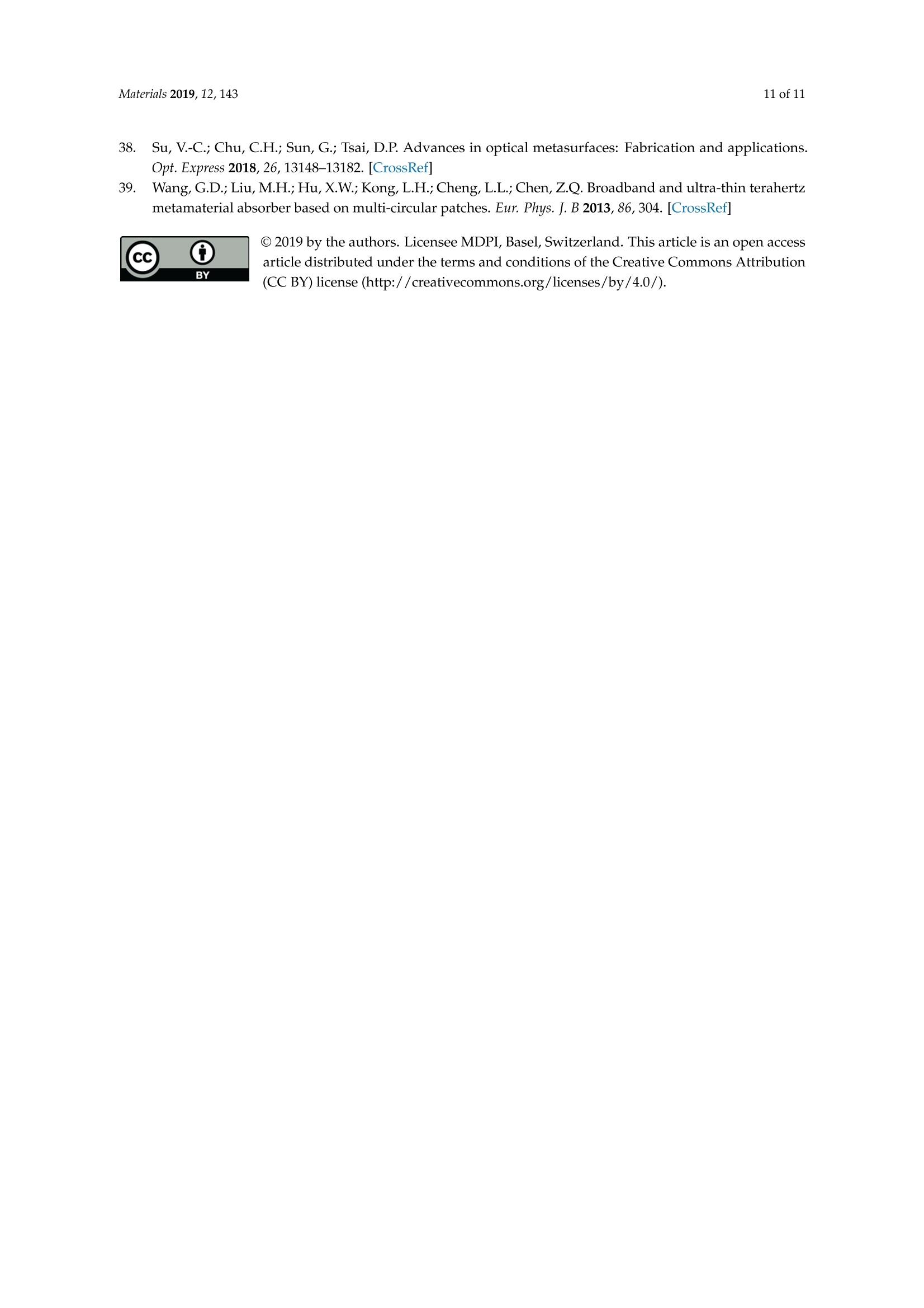
materials Materials 2019, 12, 1432 of 11 Materials 2019, 12, 143; doi:10.3390/ma12010143www.mdpi.com/journal/materials Article Tunable Perfect THz Absorber Based on a StretchableUltrathin Carbon-Polymer Bilayer Alesia Paddubskaya 1,2D, Marina Demidenko 1, Konstantin Batrakov 1,2, Gintaras Valusis ‘3Tommi Kaplas 3,4, Yuri Svirko 4,5 and Polina Kuzhir 1,2,* D 1 Institute for Nuclear Problems of Belarusian State University, Bobruiskaya 11, 220030 Minsk, Belarus;paddubskaya@gmail.com (A.P.); demidenko@inp.bsu.by (M.D.); kgbatrakov@gmail.com (K.B.) 2 Tomsk State University, 36 Lenin Prospekt, 634050 Tomsk, Russia 3 Center for Physical Sciences and Technology, Sauletekio av. 3, LT-10257 Vilnius, Lithuania;gintaras.valusis@ftmc.lt (G.V.); tommi.kaplas@uef.fi (T.K.) 4 Institute of Photonics, University of Eastern Finland, 7 Yliopistokatu, FI-80100 Joensuu, Finland;yuri.svirko@uef.fi 5 Department of Physics,M.V. Lomonosov Moscow State University, Leninskie Gory, 1199991 Moscow, Russia Correspondence: polina.kuzhir@gmail.com Received: 23 November 2018; Accepted: 26 December 2018;Published: 4 January 2019 check forupdates Abstract: By exploring the Salisbury screen approach, we propose and demonstrate a thin filmabsorber of terahertz (THz) radiation. The absorber is comprised of a less than 100 nm thick layerof pyrolytic carbon deposited on a stretchable polydimethylsiloxane (PDMS) film followed by themetal film. We demonstrate that being overall less than 200 microns thick, such a sandwich structureabsorbs resonantly up to 99.9%of the incident THz radiation, and that the absorption resonance isdetermined by the polymer thickness, which can be adjusted by stretching. Keywords: terahertz; perfect absorption; pyrolytic carbon; Salisbury screen 1. Introduction Growing interest in THz science in the last decade is due to its numerous applications in physics,astronomy, chemistry, biology, and medicine. These include THz imaging, microscopy, non-destructivetesting, tomography, medical diagnosis, health monitoring, environmental control, and chemicaland biological identification [1-3]. Most of these applications involve the detection and decoding ofultra-weak THz signals using bolometers. For example, in astronomy, THz bolometers are key elementsof Herschel Space Observatory, James Clerk Maxwell Telescope, and Stratospheric Observatory forInfrared Astronomy [4], which detect the spectra of THz radiation from space objects providing theinsights into formation and evolution of galaxies and other fundamental problems of astrophysics.To operate in open space, THz bolometers must be durable and robust, provide detection within a broadfrequency range in which the celestial objects may radiate, and comply with payload requirements. Fabrication of highly sensitive bolometers requires materials and structures with low heatcapacity [5] that can absorb almost 100%of the incident radiation. The latter implies perfect matchingof the structure impedance with the impedance of free space that can be achieved with bilayersand multi layers comprising of conductive and dielectric films. For example, the perfect absorptioncan be achieved by placing graphene sheet onto a quarter-wavelength thick dielectric substrate,when radiation comes from the substrate side [6,7]. It is worth noting that graphene (see ref. [8]for review) possesses a record-low heat capacity [9-12] and short thermal relaxation time [13].In order to match the impedance of the free space, the graphene sheet can either be placed onto epsilon-near-zero [14] material or on a dielectric film deposited on the top of a metal back reflector.The latter is referred to as the Salisbury screen approach [15-17]. To create the Salisbury screen, one needs to deposit a conductive film with a thickness smaller thanthe skin depth onto a quarter-wavelength thick dielectric layer and to place this sandwich-like structureon a metal support. However, a metallic (e.g., gold, silver or titanium) film should be a few nanometersthick. It will be highly sensitive to defects, aging, oxidation, and surface cleanliness issues [18,19].It is also impractical to replace the top conductive film with graphene because this requires it herdirect deposition [20] or transferring graphene [21] onto the dielectric support. Both techniques arestill challenging. Recently an interesting alternative to graphene for THz and microwave applications has beenproposed. It is an ultrathin film of pyrolytic carbon (PyC) [22,23] that can be directly grown on adielectric or metallic substrate. PyC films, which are comprised of disordered graphene nanoflakesplaced in the amorphous carbon host, are robust enough to be transferred, are semitransparent invisible range [24], possess high sheet conductance, and demonstrate a remarkable electromagneticinterference shielding and absorption ability in microwaves and THz [7,25]. As noted in Reference [23], it has been emphasized that DC conductivity of PyC is lower thanthat of graphene (25×104S/m and 100×104 S/m, respectively [26,27]). However, it is close to theconductivity of reduced graphene oxide (5.5×10⁴S/m) [28] and is much higher than that of pyrolyzedphotoresist (1.6×10⁴ S/m) [29]. Thus, by combining thin (<100 nm) PyC film with dielectric layersone can design a flexible and polarization-independent thin film THz absorber. In this work, we employed the Salisbury screen approach to creating THz absorber based onthin PyC films deposited on polydimethylsiloxane (PDMS) dielectric substrate. Such stretchable,flexible and mechanically robust carbon-polymer bilayer is a removable absorber of variable thicknessthat can easily stick or be removed from metallic surfaces (including polished ones) without causingany damage. We demonstrate numerically and experimentally that the structure composed of PyC,PDMS and back metal sheet can absorb up to 99.9% of the incident THz radiation and allows one totune the absorption band by stretching the polymer. 2. Theory and Numerical Simulations In order to calculate the absorption loss we considered the propagation of the linearly polarizedplane wave in the PyC/PDMS sandwich placed on the metal substrate (see Figure 1). The totalabsorptance of such a multilayer system (often referred to as Gires-Tournois etalon [30]) can becalculated as A=1- R, where R is the reflectance. If the substrate is made ofa perfect conductor(PEC), the reflectance can be obtained analytically using the continuity of tangential componentsof the electric and magnetic field sat the vacuum/PyC, PyC/polymer and polymer/PEC interfaces(see Figure 1). At normal incidence, this continuity condition yields: Here, li and l2 are the thicknesses of the PyC and dielectric layers. Respectively, E-,k; and eiare the amplitudes of the electric field, wavenumber and complex dielectric permittivity in the i-thlayer. Superscripts"+"and"-"label the forward and backward propagating waves (see Figure 1).The dielectric permittivity of the PyC film is e1(w) = iopyc/eow, where PyC conductivity opycshows a weak frequency dependence in the frequency range of interest [7]. It is worth noting that with no PEC substrate, the last equation in the system (Equation (1)) should be replaced with thefollowing equations: where E, is the complex amplitude of the transmitted wave, ko is the free space wavenumber. Figure 1. Schematic representation of the wave propagation through multilayer on a metallic substrate,PEC labels perfectly conducting substrate: (a) Salisbury screen and (b) multilayer structure also knownas Jaumann type absorber. The calculated frequency dependence of absorptance A=1-|E/E2 versus the thicknessof the polymer layer for samples with and without PyC film and a black reflector is presented inFigure 2a,b. Figure 2. Cont (e) (f) Figure 2. Frequency dependence of absorptance versus thickness of polymer layer calculated usingEquation (1) (a) with PyC layer and (b) without PyC layer at the relative permittivity of polymerof e2=2.4+0.14i, the thickness of PyC film l=100 nm and PyC conductivity pyc =4×10⁴ S/m.(c) Absorptance as a function of upuc at the PyC and polymer layer thicknesses of l1=100 nm andl2=100 um, respectively. (d) The dependence of absorptance on PyC layer thickness (l1) at thefrequency of 0.5 THz and the polymer layer thickness of l2=100 um. (e) Incidence angle dependenceof the transmittance of system for the s- and p-polarizations. (f) Incidence angle dependence of thePyC/PDMS multilayer absorptance for the s-and p-polarized waves at frequency of 0.5 THz ande2=2.4+0.14i, CPyc=4×10⁴ S/m,l1=100 nm and l2=100 um. One can observe from Figure 2a,b that there are Fabry-Perot resonances in reflectance andabsorptance spectra of PyC/polymer/PEC and polymer/PEC structures. The resonance frequenciesdepend on the polymer thickness and refractive index and not on the PyCconductivity. A bare polymerfilm placed onto PEC surface shows a poor absorption ability while depositing the PyC layer onto thepolymer significantly increases (up to 100%) the total absorptance. It is worth noting that the additionof the 100 nm thick PyC film to 100 um polymer layer left the total thickness virtually unchanged.The coincidence of frequency position of absorption peaks for samples with and without PyC filmsindicate that multiple reflections govern absorptance of the structure. In the dependence of the absorptance on the PyC conductivity shown in Figure 2c, the maximumabsorptance corresponds to the best possible(at l1=100 nm and l2=100 um) matching of the structureimpedance to the impedance of the free space. Figure 2d shows the dependence of the absorptance onthe PyC layer thickness calculated at opyc =4×10⁴ S/m and opyc =8×10+S/m. One can observethat for both conductivities there exists the optimum PyC film thickness, which provides the perfectmatching of the free space impedance and hence 100% absorptance. Figure 2e shows the dependence of the PyC/PDMS bilayer transmittance on the incidence anglefor s- and p-polarized waves calculated at the frequency of 0.5 THz for PyC film thickness of 100 nm(compare with our previous work [6]). It is worth noting that the s-polarized wave transmittancedecreases with an increase in the incidence angle, while the transmittance of the p-polarized wavetransmittance shows non-monotonous dependence on the angle of incidence. Incidence angledependence of the PyC/PDMS/PEC structure absorptance (see Figure 2d) clearly shows that forboth polarizations, such a structure is capable of absorbing more than 90% of the incident radiationprovided that the incidence angle does not exceed 50°. This implies that the proposed absorberpossesses high angle stability, which is one of the most practical important requirements. The Jaumann type absorber, which consists of several resistive layers separated by a dielectric (seeFigure 1b), is an extension of the single-layer Salisbury screen. It has been demonstrated (for example,see Reference [31]) that the addition of one extra layer makes the absorption bandwidth broaderin comparison with that of the single-layer structure. The theoretical analysis of the Jaumann typeabsorber can be performed by adding continuity conditions for extra interface to Equations (1) and (2). 3. Materials and Methods The PyC films were synthesized on 25 um thick copper foil (99.8%, Alfa Aesar, Karlsruhe,Germany) by chemical vapor deposition (CVD) in a hot wall tube furnace (30-3000C, Carbolite Gero,Neuhausen, Germany). First, the copper foil was loaded into a horizontal furnace, and the systemwas evacuated to a vacuum for up to 0.06 mBar for 1 h. Then, the substrate was heated up to 1050 °Cand annealed for 1 h. The PyC growth was carried out at 1050 °℃ by introducing the CH4 balancedin H for 30 min. The control over film thickness and roughness was attained by modification of thereaction parameters [22]. In our experiments, the ratio of hydrogen and methane was 5:20 and the totalpressure was 20 mBar. After growth, the system was cooled down to room temperature. The quality of PyC films was examined by Raman spectrometer combined with theconfocalmicroscope (Nanofinder High End, Tokyo Instruments, Belarus-Japan) with a 600 lines/mm gratingand 473 nm laser excitation. Raman spectra (Figure 3a) werecollected for samples on a copper substrateusing a 50x objective (the optical image is presented in Figure 3a). To reduce sample degradation,the average laser power was kept at 800 uW and exposition time was set to 30 s. The Raman spectrum of the PyC film in Figure 3a is dominated by two bands centered at1590 cm-1 and 1376 cm-1. The former corresponds to the vibration mode of an ideal graphite lattice(first-order G-band ~1580-1590 cm-1) and indicates the presence of the crystalline part in the PyCfilm.The latter band is a signature of the graphite disorder [31]. The ratio of intensities of these bands allowson to estimate the average size of graphite crystallites (graphene flakes) [32], which does not exceed10 nm in the fabricated PyC films. A broad band in the vicinity of 3000 cm- represents overtones ofthe one-phonon bands. Figure 3b shows a scanning electron microscopy (SEM, Helios Nanolab 650, Thermo FisherScientific, Hillsboro, OR, USA) image (tilt view) of PyC film synthesized on the copper substrate.To measure the film thickness and investigate the cross-section of the carbon film, a thin Pt layer with athickness of about 100 nm was deposited on the surface of the selected areas to avoid any damage tothe PyC film. The surface was milled using a dual beam-FIB (FEI Helios NanoLab 650, Thermo FisherScientific, Hillsboro,OR, USA) and then imaged by the SEM with tilt 54° (see Figure 3c). The contrastdifference between Pt/carbon and carbon/copper interfaces indicates that the PyC film thicknessvaries in the range 80-100 nm over the sample surface. One may also conclude from Figure 3c that thethicker the PyC film, the weaker adhesion that results in film roughness (see Figure 3a). (a) (b) Figure 3. (a) The optical image of the surface of the PyC film on the copper substrate and Raman spectraof the PyC film. Fitting (solid green line) shows D (disorder), G (C-C vibration mode), D'(inter-valleyphonon scattering) and D" (the localized vibrational modes of the impurities can interact with theextended phonon modes of graphene resulting in the observed splitting) bands [33]. (b) SEM image(tilt view 53°) of the PyC film on the top of the copper substrate. (c) SEM image of the cross-sectionPyC film on copper substrate with the deposited~100 nm thick Pt layer. The Pt layer (top), PyC film(middle, 101 nm), the sputtering copper layer (bottom, 43.07 nm), the cavity between carbon layer andcopper foil. In order to create the Salisbury screen, we deposited the PyC film on a flexible and stretchablesubstrate, which was fabricated by mixing the liquid PDMS prepolymer with a cross-linking curingagent at a 10:1 volume ratio (Sylgard 184 silicone elastomer, Dow Corning), pouring into the specialform and curing at 80 °C for 15 min. The thickness of the obtained PDMS films was monitored bymeasuring the THz transmittance spectra. Due to weak adhesion to the copper substrate, the PyC film with a thickness of about 100 nmcan be easily transferred onto PDMS using dry transfer technique [34], which is presented in Figure 4.A 1 cm x1 cm PyC/copper piece was placed PyC-face down on the PDMS film with thickness from100 up to 200 um (step 1). The copper foil was gently pressed using a Teflon roller to make the PyC filma:1Aydhere to the PDMS surface (step 2). The copper foil was easily removed by lifting without significantdamage to the PyC film (step 3). The obtained PyC/PDMS flexible assembly was attached to a SiO2substrate with a thin gold film deposit on top (PyC/PDMS/gold sample). In the case of Jaumann typeabsorber, the procedure could be repeated several times. immmmmm Figure 4. The process of PyC dry transfer to PDMS. 4. Results The electromagnetic response of our film in THz frequency range was measured using acommercial THz time-domain spectrometer (T-Spec, EKSPLA, Vilnius, Lithuania), in which THzradiation with frequency up to 2 THz is generated by a photoconductor antenna (low temperaturegrown GaBiAs) under irradiation with 50-150 fs long laser pulses at wavelength of 1050 nm and powerof about 50 mW. The THz pulses were detected by a similar photoconductive antenna. The spectrometerhas a module design, i.e., depending on the task it allows one to measure either transmittance orreflectance spectra. The dent helps to put each module exactly in the same place every time. In order toincrease the signal to noise ratio, each spectrum was averaged over 1024 measurements. Fast Fouriertransform was used to convert the time-domain signal into the frequency domain. To introduce auniform tensile strain, we used a linear pulse motor. Figure 5a,b shows the THz reflectance spectra of 145 um and 167 um thick PyC/PDMS sandwiches(referred to as "first" and"second"bilayers, respectively) and for combined structure, in which"first"and "second"bilayers are combined into a single multilayer structure. The absorptance spectra forall structures are presented in Figure 5c. The measurement was performed in the frequency range0.1-1.1 THz that corresponds to the maximum signal-to-noise ratio. One can see that absorptance ofPyC/PDMS/gold Salisbury screen exceeds 99.9% at certain frequencies, which depend on the PDMSlayer thickness. Figure 5b shows that the addition of the extra bilayer leads to an increase in the totalbandwidth while the total absorptance decreases. However, it has been shown in [7] that there existsan optimum combination of the PyC film thickness and the number of the PyC/PDMS bilayers thatallow one to achieve simultaneously strong absorption and broad bandwidth. Figure 5. Reflectance (a,b), and absorptance spectra (c) of PyC/PDMS/gold and PyC/PDMS/PyC/PDMS/gold sandwich-like structures, respectively. Numerical calculations were performedby solving Equation (1) with the following material parameters: lPyc=100 nm, lpDMS1=145 um,lPDMS2=167 um,0Puc=3×10⁴ S/m,ePDMS =2.3 + 0.12i. (d) Frequency dependence of transmittanceof PyC/PDMS bilayers vs. the applied strain. Inset shows the calculated PyC conductivity as a functionof the unidirectional strain. The thickness of the PyC/PDMS bilayer can be changed by applying tensile strain to the PDMS.Our Raman measurements (the results are not presented here) confirm that stretching of the PDMSdoes not change the Raman spectrum of the deposited PyC film. Dependence of the PyC/PDMS THztransmittance spectrum on the applied tensile strain is presented in Figure 5d. By comparing ourexperimental data with the solution of Equation (1) and by considering that the PDMS Poisson ratio is0.48 [35], we revealed the dependence of the AC conductivity of PyC film on the tensile strain. One canobserve from the inset to Figure 5d that opyc does not change for the strain for up to 15%. At theextension to the original length for up to 30%, the PyC conductivity decreases by about 8% leavingthe THz response of the PyC film virtually unchanged. However, the stretching shifts Fabry-Perotresonances because of the decrease in the PDMS thickness, which allows the tuning of the absorptanceand transmittance spectra of the PyC/PDMS bilayer. Figure 6 shows the measured dependence of the PyC/PDMS bilayer transmittance on the angleof incidence for s-and p-polarized waves in the frequency range 0.1-1.1 THz and comparison ofsimulation and experimental data at frequencies of 0.5 and 0.8 THz. One can see a good correspondencebetween experimental and theoretical results. It is also worth noting that this correspondence indirectlyconfirms a remarkable angle insensitivity of the PyC/PDMS-based Salisbury screen. 0.80 0.30 0.80 (c) (d) Figure 6. Contour plot of the PyC/PDMS bilayer transmittance for the(a) s-and (b) p-polarized waveson the frequency/angle of incidence plane (experimental data). The incidence angle dependence ofthe PyC/PDMS transmittance at 0.5 and 0.8 THz for the (c) s-and (d) p-polarizations. Circles andsolid lines show, respectively, experimental data and results of numerical simulation at lPyc=100 nm,lpDMs =200 um,Cpvc=3.2×10⁴S/m, EpDMs =2.3 +0.12i. 5. Conclusions Since the proposed thin sandwich-like structure does not require any patterning orpost-processing, and demonstrates the comparable absorptance ability with existing ultrathin THz absorbers [36-39], our results open an interesting opportunity to fabricate a tunable thin film THzabsorber that maintains fabrication simplicity and low cost, has a small thickness and low weight,and offers possibility of integration into the silicon platform. The demonstrated PyC based Salisburyscreen possesses a remarkable absorption ability at THz frequencies and can be used as a workingelement for THz bolometers for aeronautics, as well as in THz transmission imaging, tomography andmicroscopy systems. Author Contributions: Conceptualization, A.P. and P.K.; methodology, A.P., K.B., and G.V.; formal analysis, A.P.,Y.S., and G.V.; investigation, A.P., M.D., T.K., and P.K.; data curation, A.P., K.B.; validation, Y.S.; writing-originaldraft preparation, A.P. and P.K.; writing-review and editing, Y.S.,A.P., T.K., and G.V.;visualization, A.P.; projectadministration, P.K., Y.S. Funding: This research was supported by H2020-GA644076 RISE project CoExAN, the Union State Technology-SGprogram, and RFBR grant 16-02-00684. Acknowledgments: A.P., K.B., and P.K. are thankful for the support by Tomsk State University CompetitivenessImprovement Program. Conflicts of Interest: The authors declare no conflict of interest. References ( 1, T onouchi, M. Cutting-edge terahertz t echnology. Nat. Photonics 2007,1,97-105.[C r o ssRef] ) ( 2. Siegel, P.H. THz I nstruments for Space. IEEE Trans. A n tennas Pr o pag. 2007,55,2957-2965. [Cro s s Ref] ) ( 3. Nagatsuma, T. Terahertz technologies: Present and future. IE I CE Ele c tron. Express 2011, 8, 11 2 7-1142. 「 CrossRef l ) ( 4. Richards, P.L.;Mc Creight, C.R. Infrared De t ectors for Astrophysics. Phys. Today 2005,58, 41-47.[CrossR e f ] ) ( 5. Dhillon, S.S.; Vitiello, M.S.; Linfield,E.H.; Davies, A.G.; Hoffmann,M.C.; Booske,J; Paoloni, C.;Gensch, M.;Weightman, P.; W i lliams, G.P . The 20 1 7 terahertz science and tec h nology roadmap. J. Phys. D Appl. Phys.2017,50. [ CrossRef] ) ( 6. Batrakov, K.; Kuzhir, P. ; Maksimenko, S .; Volunets, N.; Voronovich, S.; Paddubskaya, A.; V alusis, G.; Kaplas, T.; Svirko, Y.; Lambin, P . E nhanced microwave-to-terahertz absorption in grap h ene. Appl. Ph y s. Lett. 2016,108,123101.[ CrossRe f ) ( 7. Kuzhir,P.; Paddubskaya, A.; Volynets,N.; Batrakov, K.; Kaplas,T.;Lamberti,P.; Kotsilkova, R.; Lambin, P. Main principles of passive devices based on graphene and carbon films in microwave-THz frequency range. J. Nanophotonics 2017 , 11,032504.[C rossRef ] ) ( 8. Walker, R.C.; Shi, T.; Silva, E.C.; Jovanovic, I .; Robinson, J.A. Radiation effects on two-dimensional mat e rials.Phys. Status Solidi A 2016,213,3065-3077.[Cr o s s R ef ) ( 9. Fong,K.C.; Schwab,K.C. Ultrasensitive and Wide-Bandwidth Thermal Measurements of Graphene at LowTemperatures. Phys. Rev. X 2012,2,031006.[Cr o s sRef] ) ( 10. Balandin, A.A. Thermal properties of graphene and nanostructured carbon materials. Nat. Mater. 2 011, 1 0,569-581. [ CrossRef] ) ( 11. Fong, K.C.; Wollman, E.E.; Ravi, H.; Chen, W.; Clerk, A.A.; Shaw, M.D.; Leduc, H.G.; Schwab, K.C.Measurement of the Electronic Thermal Conductance Channels and Heat Capacity of Graphene at LowTemperature. Phys.R e v. X 2013,3,041008. [Cr o s s R ef] ) ( 12. Crossno,J.; Shi, J.K.; Liu, X.;Harzheim, A.; Lucas, A.; Sachdev, S.; Kim, P. Observation of the Dirac fluid andthe breakdown of the Wiedemann-Franz law in graphene. Science 2016,351,1058-1061. [Cr ossRef] ) ( 13. Koppens, F.H.L.; M u eller, T.; Avouris, P.; Ferrari, A .C.; V itiello, M.S.; Polini, M. Photodetectors basedon graphene, other t wo-dimensional m a terials and hybrid systems. N a t. N a notechnol. 2 0 14, 9,7 8 0-793. [ C r ossRe f ] [Pu b M e d ] ) ( 14. Lobet, M .; M ajerus, B .; Henrard, L.; Lambin, P. Perfect electromagnetic absorption u sing graphene and epsilon-near-zero metamaterials. Phys. Rev. B 2016,93,235424.[C rossRef] ) ( 15. Bauer, S.;Bauer-Gogonea,S.; Ploss, B. The physics of pyroelectric infrared devices. Appl. Phys. B 1992, 54,544-551. [ C r ossRef] ) ( 16. Min Woo,J.; Kim, M.-S.; Ki m , H.W.; Jang, J.-H. Graphene based salisbury screen for terahertz absorber. Appl. Phys. Lett . 2014,104,081 1 06. [ Cross R ef ] ) ( 17. Li, W.; Jin, H.; Zeng, Z.; Zhang, L.;Zhang, H.;Zhang, Z. Flexible and easy-to-tune broadband electromagnetic wave absorber based on carbon resistive film sandwiched by silicon rubber/multi-walled carbon nanotube composites. Carbon 2017,121,544-551. [Cr ossRe f ] ) ( 18. Kroll, J.;Darmo, J.; U n terrainer, K. High-performance tera h ertz elec t ro-optic detector. Elec t ron. Lett. 2004, 40,763-764.[ CrossRef ) ( 19. Zhou, D.-X.; Parrott, E.P.J.; Paul, D.J.; Zeitler, J.A . Determination of complex refractive index of t hi n metalfilms from terahertz time-domain spectroscopy. J. App. Phys. 2008,104,053110. [C r ossRef ] ) ( 20. Ismach, A.; D ruzgalski, C . ; P e nwell, S.; S c hwartzberg, A. ; Zh e ng, M.; Javey, A.; Bok o r, J.; Zhang, Y. Direct chemical vapor deposition of graphene on d ielectric surfaces. Nan o Lett . 201 0 , 10, 1 542-1548. T C r ossRe f l ) ( 22. 2 . Kaplas,T.; Svirko, Y. Direct deposition of semitransparent conducting pyrolytic carbon films. J. Nanophotonics2012, 6,061703.[ CrossRe f ] ) ( 23. McEvoy,N.;Peltekis, N.; Ku m ar, S.; Rezvani,E.;N o lan, H.; Keeley, G.P.; Blau, W.J.;Du e sberg, G.S. Synthesisand analysis of thin conducting pyrolytic carbon films. Carbon 2012, 50, 1216-1226. [Cro s s R e f] ) ( 24. Kaplas, T.; Kuzhir, P.Ultra-thin Graphitic Film: S ynthesis and Physical Properties. Nanoscale Res. L e tt. 2016,11,54. [ C rossRe f ] [PubMed ] ) ( 25. Batrakov, K.; Kuzhir, P.; Maksimenko, S.;Paddubskaya,A.; Voronovich, S.; Kaplas, T.; Svirko, Y. Enhancedmicrowave shielding effectiveness of ultrathin pyrolytic carbon films. Appl. Phys. Lett. 20 1 3,103,073117. 「 CrossRef l ) ( 26. Doherty, E . M.;De, S.; Lyon, P.E.; Nirmalraj, P.N.;Scardaci, V.; Joimel, J.;Blau, W.J.; Boland, J.J.; Coleman, J.N. The spatial uniformity and electromechanical stability of transparent, conductive films of single walled nanotubes. Carbon 2009, 47, 2466-2473. [ CrossRef] ) ( 27. Bae, S.; Kim, H.; Lee, Y.; Xu, X.; P ark, J.-S.; Zheng, Y.; Balakrishnan, J; Lei, T.; Kim, H.R.; Song, Y.; et al.Roll-to-roll production of 30-inch graphene films for transparent electrodes. Nat. Nanotech. 2010,5,574-578.[ C r ossRef] [ P ub M ed] ) ( 28. Wang, X.; Zhi, L.; Mullen, K. Transparent, Conductive Graphene E l ectrodes f o r Dye-Sensitized Solar Cells. Nano Lett. 2007,8,323-327.[C rossRef] ) ( 29. Schreiber, M.; Lutz, T.;Keeley, G.P.; Kumar, S.; Boese, M.; Krishnamurthy, S.;Duesberg, G.S. Transparent ultrathin conducting carbon films. Appl. Surf. Sci. 2010, 256, 6186-6190. [ C ro ssR e f ] ) ( 30. Gires, F.; Tournois,P.R. Interferometre utilisable pour la compression d'impulsions lumineuses modulees en frequence. Acad. Sci. P aris 1964, 258,6112-6615. ) ( 31. Chamber,B.; Tennant, A. Optimised design of Jaumann radar absorbing materials using a genetic algorithm.IEEE Proc. Radar Sonar Navig. 1996,143,23-30. [ CrossRef ] ) ( 32. Sadezky, A.; M uckenhuber, H.; Grothe, H.;Nie s sner, R.; Poschl, U. Raman Micr o spectroscopy of Soot and Related Carbonaceous Materials: Spectral Analysis and Structural Information . Carbon 2005,43,1731-1742. [ C r ossRe f l ) ( 33. Childres, I .; Jauregui, L.A.; Park, W.; Cao, H.; Chen, Y.P. Raman Spectroscopy of Graphene and Relate d Materials. Available online : https://www.physics.pu r du e .edu/quantum / files/Raman_Spectr o sco p y_of_Graphen e _N O VA_Ch i ldr e s . pdf ( a c cessed on 30 October 2013). ) ( 34. Cancado, L.G.; T a kai, K . ; Enoki, T. G e neral equation for the determination of t h e crys t allite size La ofnanographite by Raman spectroscopy. Appl. Phy s . Let t . 2006,88,163106. [Cros s R e f ] ) ( 35. Kaskela, A.; Nasibulin, A.G.; Timmermans, M.Y.; Aitchison, B.; Papadimitratos, A.; Tian,Y.;Z h u, Z.; Jiang, H.;Brown, D.P.;Zakhidov, A.; et al. Aerosol-Synthesized SWCNT Networks with Tunable Conductivity and T ransparency by a Dry Transfer Technique. Nano Lett. 2010,10, 4349-4355. [C rossRef ] [ PubM ed ] ) ( 36. Johnston, I.D.;McCluckey, D.K.; Tan, C.K.L.; Trancey, M.C. Me c hanical characterization of bulk Sylgard 184for microfluidics and microengineering. J. Micromech. Mic r oeng. 2014, 24,035017. [Cros s R ef] ) ( 37. Kats, M.A.; Blanchard, R.; Genevet, P.; Capasso, F.Na n ometre optical coatings based on strong interferenceeffects in highly absorbing media. Nat. Mater. 2013,12,20-24. [Cr ossRef] ) 38. Su, V.-C.; Chu, C.H.; Sun, G.; Tsai, D.P. Advances in optical metasurfaces: Fabrication and applications.Opt. Express 2018, 26,13148-13182. [CrossRef] 39. Wang, G.D.; Liu, M.H.; Hu, X.W.; Kong, L.H.; Cheng, L.L.; Chen, Z.Q. Broadband and ultra-thin terahertzmetamaterial absorber based on multi-circular patches. Eur. Phys. J. B 2013,86, 304.[CrossRef] @ 2019 by the authors. Licensee MDPI, Basel, Switzerland. This article is an open accessCcarticle distributed under the terms and conditions of the Creative Commons Attribution(CC BY) license (http://creativecommons.org/licenses/by/4.0/). By exploring the Salisbury screen approach, we propose and demonstrate a thin filmabsorber of terahertz (THz) radiation. The absorber is comprised of a less than 100 nm thick layer of pyrolytic carbon deposited on a stretchable polydimethylsiloxane (PDMS) film followed by the metal film. We demonstrate that being overall less than 200 microns thick, such a sandwich structure absorbs resonantly up to 99.9%of the incident THz radiation, and that the absorption resonance is determined by the polymer thickness, which can be adjusted by stretching.
确定
还剩9页未读,是否继续阅读?

产品配置单
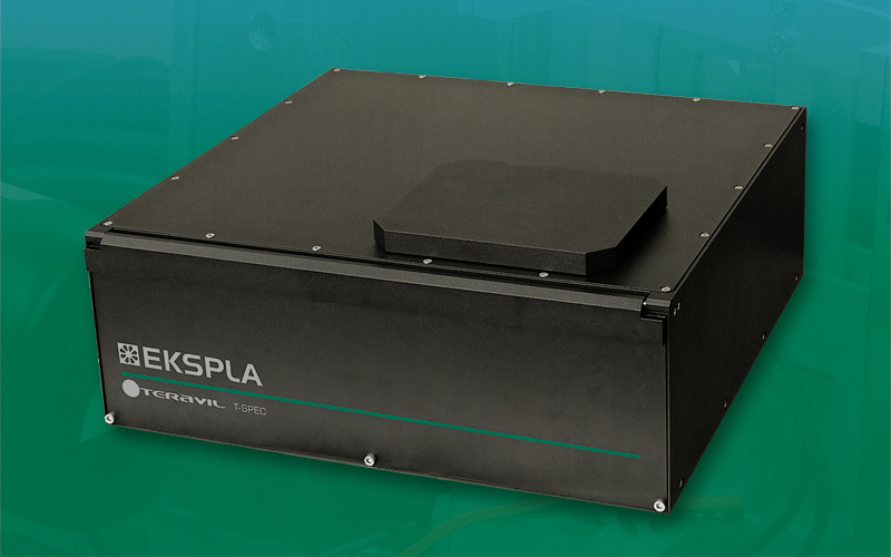
北京欧兰科技发展有限公司为您提供《超薄碳聚合物双层中太赫兹时域光谱检测方案(其它光谱仪)》,该方案主要用于其他中理化分析检测,参考标准--,《超薄碳聚合物双层中太赫兹时域光谱检测方案(其它光谱仪)》用到的仪器有Ekspla T-SPEC 实时太赫兹(THz)光谱仪
推荐专场
相关方案
更多
该厂商其他方案
更多