


方案详情
文
Introduction
There is increasing need for the micro-analyst to correctly determine chemical composition of regions
on the sub-micron scale. Field emission SEMs offer an ideal tool for these tasks due their excellent
spatial resolution and high brightness sources. However, in order to analyze these types of samples the
accelerating voltage of the electron beam is commonly in the range 1-5kV. Traditionally when working
at these voltages low count rates necessitated the use of EDS detectors with large crystals to maximize
collection solid angle. Analysis using EDS at low kV is, however, complicated by the large number of
overlapped X-ray lines seen in this part of the spectrum. New field emission SEMs that offer high
currents at low kV are opening new opportunities to use the higher spectral resolution and sensitivity
of WDS to analyze samples on the sub-micron scale.
方案详情

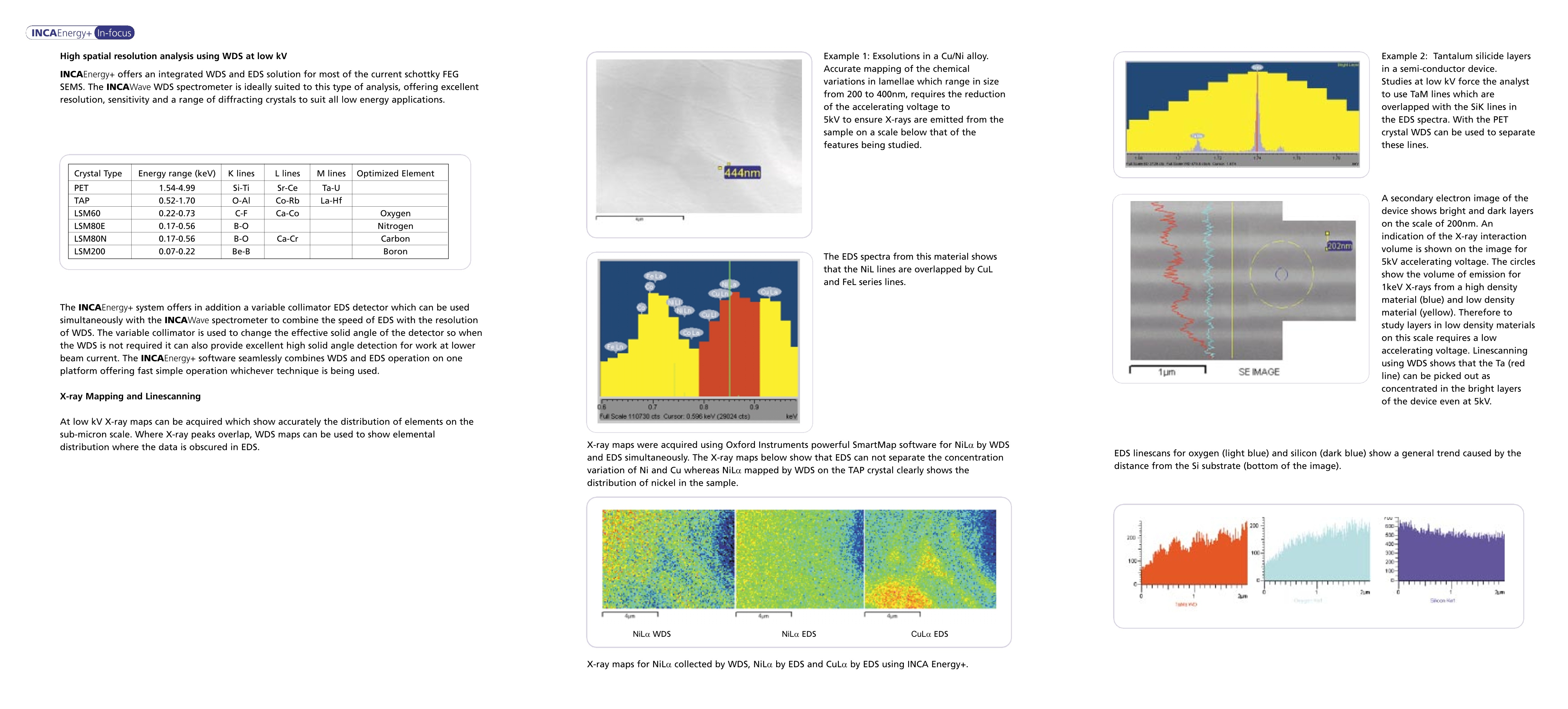
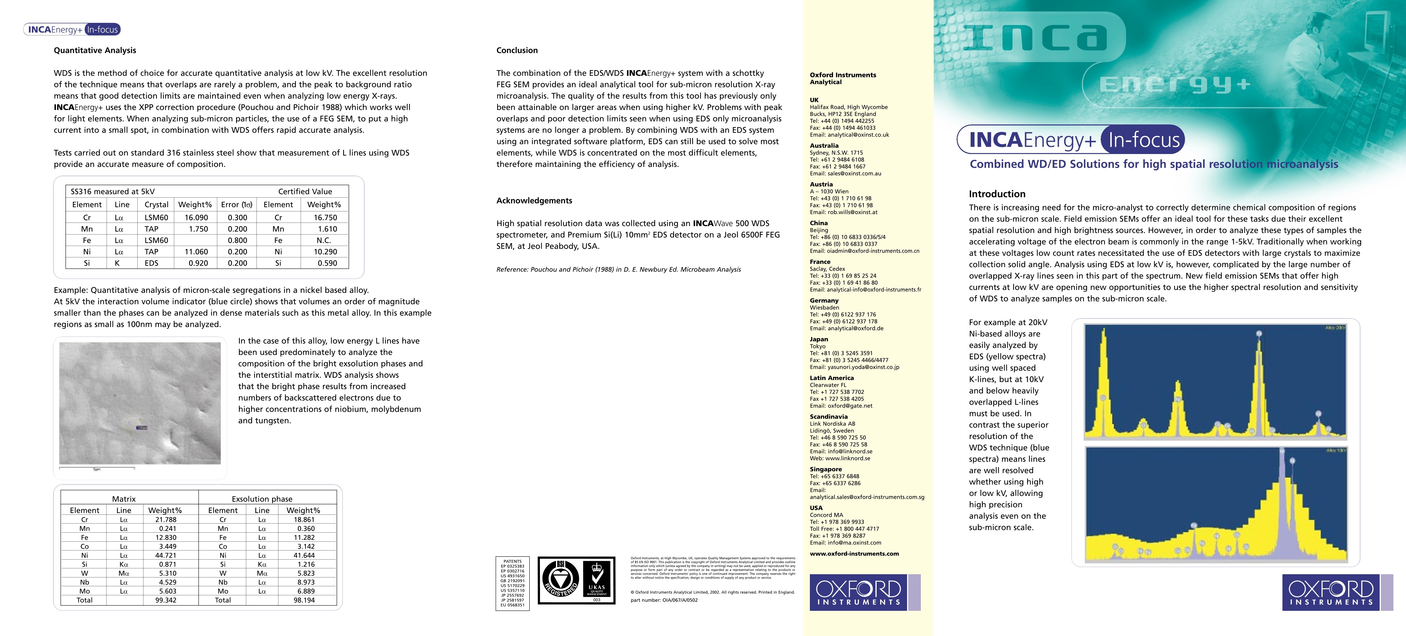
(INCAEnergy+In-focus 03cnca(INCAEnergy+i-In-focusQuantitative AnalysisX-ray maps for NiLa collected by WDS, NiLa by EDS and CuLo by EDS using INCA Energy+. High spatial resolution analysis using WDS at low kV INCAEnergy+ offers an integrated WDS and EDS solution for most of the current schottky FEGSEMS. The INCAWave WDS spectrometer is ideally suited to this type of analysis, offering excellentresolution, sensitivity and a range of diffracting crystals to suit all low energy applications. Crystal Type Energy range (keV) K lines L lines M lines Optimized Element PET 1.54-4.99 Si-Ti Sr-Ce TTa-U TAP 0.52-1.70 O-AI Co-Rb La-Hf LSM60 0.22-0.73 C-F Ca-Co Oxygen LSM80E 0.17-0.56 B-O Nitrogen LSM80N 0.17-0.56 B-O Ca-Cr Carbon LSM200 0.07-0.22 Be-B Boron The INCAEnergy+ system offers in addition a variable collimator EDS detector which can be usedsimultaneously with the INCAWave spectrometer to combine the speed of EDS with the resolutionof WDS. The variable collimator is used to change the effective solid angle of the detector so whenthe WDS is not required it can also provide excellent high solid angle detection for work at lowerbeam current. The INCAEnergy+ software seamlessly combines WDS and EDS operation on oneplatform offering fast simple operation whichever technique is being used. X-ray Mapping and Linescanning At low kV X-ray maps can be acquired which show accurately the distribution of elements on thesub-micron scale. Where X-ray peaks overlap, WDS maps can be used to show elementaldistribution where the data is obscured in EDS. Example 1: Exsolutions in a Cu/Ni alloy. Accurate mapping of the chemical variations in lamellae which range in size from 200 to 400nm, requires the reduction of the accelerating voltage to 5kV to ensure X-rays are emitted from the sample on a scale below that of the features being studied. 444nm The EDS spectra from this material showsthat the NiL lines are overlapped by CuLand FeL series lines coLa Ee 0.7 Full Scale 110730 cts Cursor:0.596keV (29024 cts) X-ray maps were acquired using Oxford Instruments powerful SmartMap software for NiLo by WDSand EDS simultaneously.The X-ray maps below show that EDS can not separate the concentrationvariation of Ni and Cu whereas NiLa mapped by WDS on the TAP crystal clearly shows thedistribution of nickel in the sample. Example 2: Tantalum silicide layersin a semi-conductor device.Studies at low kV force the analystto use TaM lines which areoverlapped with the SiK lines inthe EDS spectra. With the PETCIcrystal WDS can be used to separatethese lines. A secondary electron image of thedevice shows bright and dark layerson the scale of 200nm. Anindication of the X-ray interactionvolume is shown on the image for5kV accelerating voltage. The circlesSsIhow the volume of emission for1keV X-rays from a high densitymaterial (blue) and low densitymaterial (yellow). Therefore tostudy layers in low density materialson this scale requires a lowaccelerating voltage. Linescanningusing WDS shows that the Ta (redline) can be picked out asconcentrated in the bright layersof the device even at 5kV. EDS linescans for oxygen (light blue) and silicon (dark blue) show a general trend caused by thedistance from the Si substrate (bottom of the image). WDS is the method of choice for accurate quantitative analysis at low kV. The excellent resolutionof the technique means that overlaps are rarely a problem, and the peak to background ratiomeans that good detection limits are maintained even when analyzing low energy X-rays.INCAEnergy+ uses the XPP correction procedure (Pouchou and Pichoir 1988) which works wellfor light elements. When analyzing sub-micron particles, the use of a FEG SEM, to put a highcurrent into a small spot, in combination with WDS offers rapid accurate analysis. Tests carried out on standard 316 stainless steel show that measurement of L lines using WDSprovide an accurate measure of composition. SS316 measured at 5kV Certified Value Element Line Crystal Weight% Error (1o) Element Weight% Cr La LSM60 16.090 0.300 Cr 16.750 Mn La AP 1.750 0.200 Mn 1.610 Fe La LSM60 0.800 Fe N.C. Ni LO TAP 11.060 0.200 Ni 10.290 Si K EDS 0.920 0.200 Si 0.590 Example: Quantitative analysis of micron-scale segregations in a nickel based alloy.At 5kV the interaction volume indicator (blue circle) shows that volumes an order of magnitudesmaller than the phases can be analyzed in dense materials such as this metal alloy. In this exampleregions as small as 100nm may be analyzed. In the case of this alloy,low energy L lines havebeen used predominately to analyze thethat the bright phase results from increasedand tungsten. Element Line Weight% Element Line Weight% 21.788 Cr 18.861 0.241 Mn Mn La 11.282 Fe CoNi La La 3.142 La 44.721 41.6441.216 Si KaMa KaMa 5.823 Nb La 4.529 Nb La 8.973 Lc 5.60399.342 Mo Total La 6.88998.194 Total Conclusion The combination of the EDS/WDS INCAEnergy+system with a schottkyFEG SEM provides an ideal analytical tool for sub-micron resolution X-raymicroanalysis. The quality of the results from this tool has previously onlyybeen attainable on larger areas when using higher kV. Problems with peakoverlaps and poor detection limits seen when using EDS only microanalysissystems are no longer a problem. By combining WDS with an EDS systemusing an integrated software platform, EDS can still be used to solve mostelements, while WDS is concentrated on the most difficult elements,therefore maintaining the efficiency of analysis. Oxford InstrumentsAnalyticaall UK Halifax Road, High WycombeBucks, HP12 3SE England : +44(0) 1494 飞Tel: +44(0) 1494 442255lei.FEax: +44 (0) 1494 461033 Email: analytical@oxinst.co.uk Australia Sydney, N.S.W. 1715 Tlel: +61 2 94846108FEax: +61 2 9484 1667Email: sales@oxinst.com.au Austria A-1030\Wier AAcknowledgements T飞ell:: ++4433 (0) 1 710 61 98 l Fax: +43 (0) 1 710 61 98 Email: rob.wills@oxinst.at High spatial resolution data was collected using an INCAWave 500 WDS spectrometer, and Premium Si(Li) 10mm²EDS detector on a Jeol 6500F FEGSEM, at Jeol Peabody, USA. Reference: Pouchou and Pichoir (1988) in D. E. Newbury Ed. Microbeam Analysis ChinaBeijingTel· +86Tell:: +86 (0)10 6833 0336/5/4Fax: +86 (0) 10 6833 0337Email: oiadmin@oxford-instruiFranceSaslay Cede Tel+:33(0)1 f+333(0) 1 69 85 25 24 l:+3Fax:++33 (0) 1 69 41 86 80Email: analytical-info@oxford-instrunents.frGermany Wieshaden Tall·.iTel: +49 (0) e) 61122 937 176Fax: +49 (0) 6122 937 178 Email: analytical@oxford.de Japan Tkyn lokkyyo Tel: +81 (0) 3 5245 3591Fax: +81 (0) 35245 4466/4477 . Email: yasunori.yoda@oxinst.co.jr.jp Latin America learwaterTel: +1 727 538 7702 Fax+1 727 538 4205EEnmaili:l:ooxford@iagaatte.et Scandinavia Link Nordiska Al Lidingo, Sweden Tel:+46 8 590 725 5C Fax: +46 8 590 725 58FmaEmail: info@lirinkiknord.si Web: www.linknord.se Singapore SeTel 飞: +65 6337 6848Fax: +65 6337 6286 Fmnaail: analytical.sales@oxford-i its.com.sg . USA Concord MA Tel: +1 978 369 9933 rall Fron80n Toll Free: +1 800 447 4717Fax: +1 978 369 8287 Email: info@ma.oxinst.com www.oxford-instruments.com TENTS UsP 0302716 UISS 51 /S 535711C P 2557692 P2581597 Energyl+ INCAEnergy+In-focus Combined WD/ED Solutions for high spatial resolution microanalysis Introduction There is increasing need for the micro-analyst to correctly determine chemical composition of regionson the sub-micron scale. Field emission SEMs offer an ideal tool for these tasks due their excellentspatial resolution and high brightness sources. However, in order to analyze these types of samples theaccelerating voltage of the electron beam is commonly in the range 1-5kV.Traditionally when workingat these voltages low count rates necessitated the use of EDS detectors with large crystals to maximizecollection solid angle. Analysis using EDS at low kV is, however, complicated by the large number ofoverlapped X-ray lines seen in this part of the spectrum. New field emission SEMs that offer highcurrents at low kV are opening new opportunities to use the higher spectral resolution and sensitivityof WDS to analyze samples on the sub-micron scale. For example at 20kVNi-based alloys are easily analyzed by EDS (yellow spectra)using well spacedK-lines, but at 10kVand below heavilyoverlapped L-linesmust be used. Incontrast the superiorresolution of theWDS technique (bluespectra) means linesare well resolvedwhether using highor low kV, allowinghigh precisionanalysis even on thesub-micron scale. IntroductionThere is increasing need for the micro-analyst to correctly determine chemical composition of regionson the sub-micron scale. Field emission SEMs offer an ideal tool for these tasks due their excellentspatial resolution and high brightness sources. However, in order to analyze these types of samples theaccelerating voltage of the electron beam is commonly in the range 1-5kV. Traditionally when workingat these voltages low count rates necessitated the use of EDS detectors with large crystals to maximizecollection solid angle. Analysis using EDS at low kV is, however, complicated by the large number ofoverlapped X-ray lines seen in this part of the spectrum. New field emission SEMs that offer highcurrents at low kV are opening new opportunities to use the higher spectral resolution and sensitivityof WDS to analyze samples on the sub-micron scale.
确定
还剩1页未读,是否继续阅读?

产品配置单
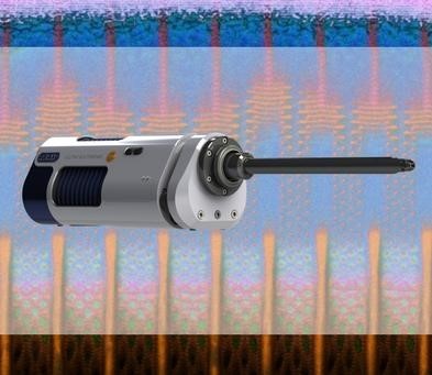
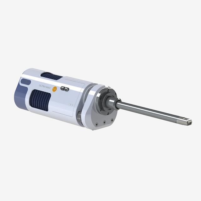
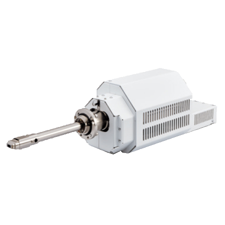
牛津仪器科技(上海)有限公司为您提供《材料中高空间分辨率显微分析检测方案(扫描透射电镜)》,该方案主要用于其他中理化分析检测,参考标准--,《材料中高空间分辨率显微分析检测方案(扫描透射电镜)》用到的仪器有牛津仪器Ultim Extreme无窗超级能谱
推荐专场
相关方案
更多
该厂商其他方案
更多