


方案详情
文
Introduction
Historically energy dispersive X-ray spectroscopy has been focused towards high energies where X-ray lines are well separated
and the X-ray background is low. Recently the demand for higher spatial resolution, whether that is when analysing
semiconductor devices or measuring precipitates in metals, has increased dramatically. To ensure maximum sensitivity when
working under these demanding conditions the Ultim® range of EDS detectors combine the largest area SDD with optimised
geometries to consistently deliver a higher count rate.
方案详情

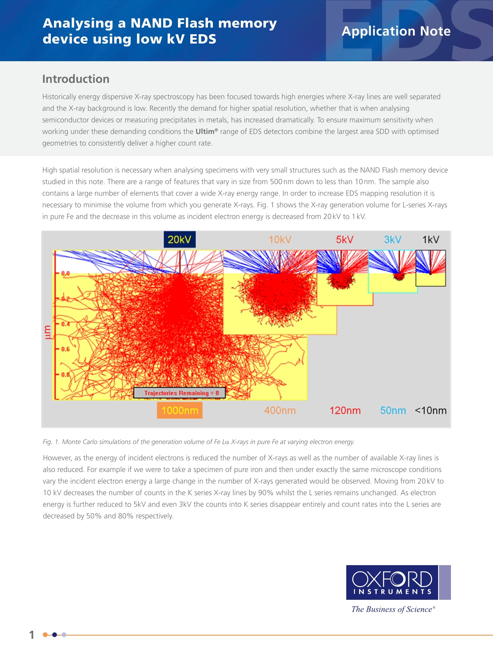
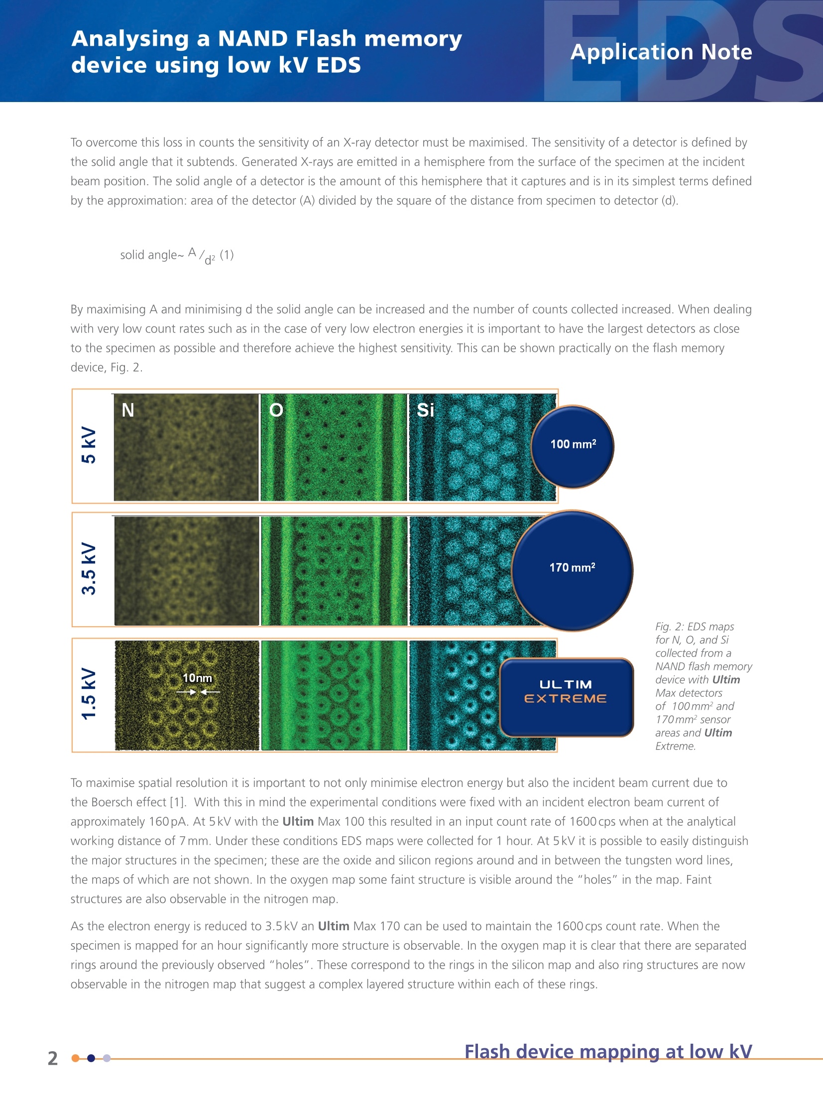
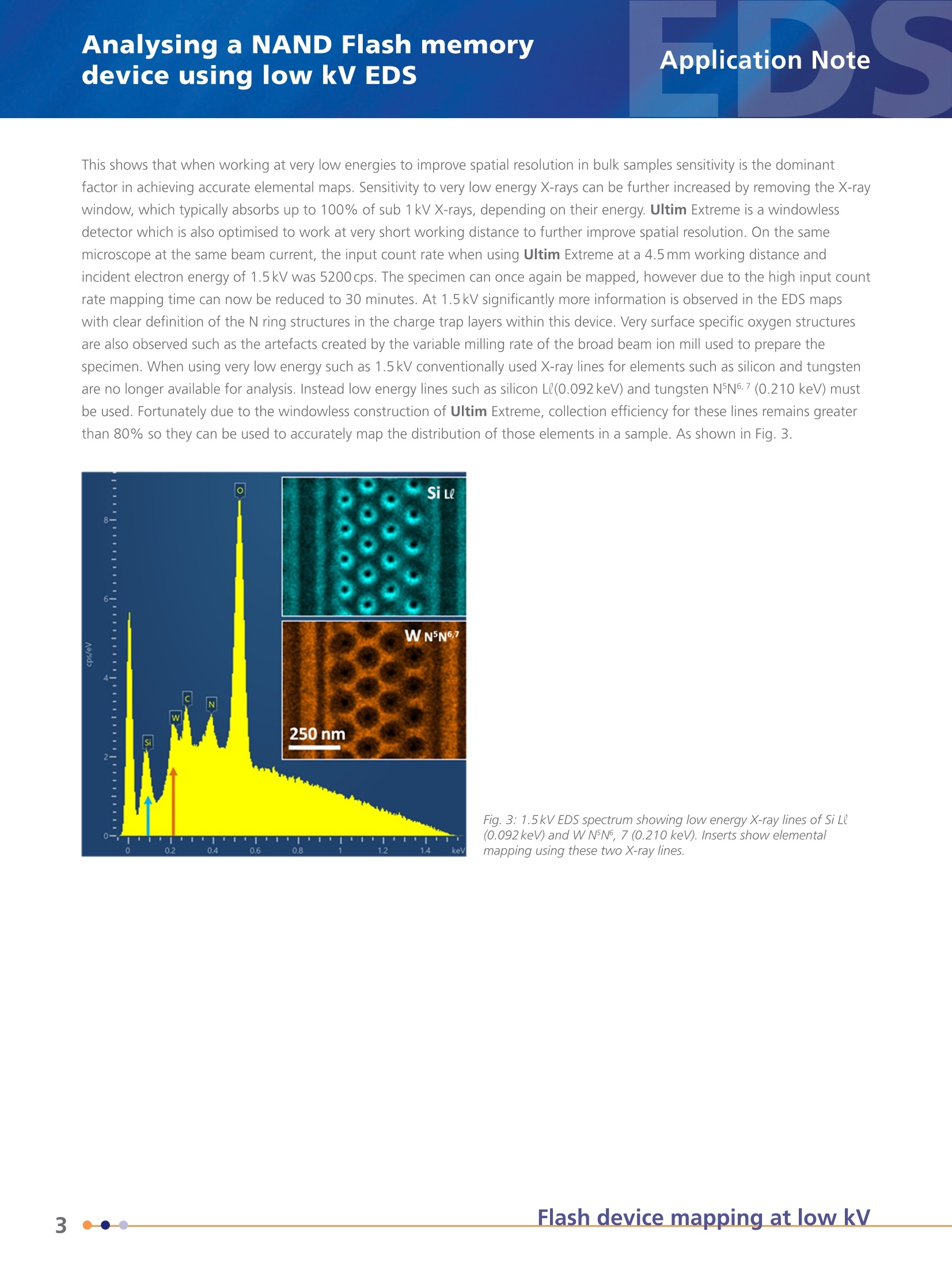
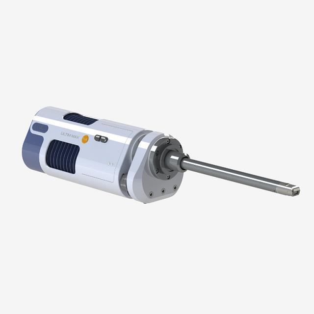
Application Note Analysing a NAND Flash memorydevice using low kV EDS Introduction Historically energy dispersive X-ray spectroscopy has been focused towards high energies where X-ray lines are well separatedand the X-ray background is low. Recently the demand for higher spatial resolution, whether that is when analysingsemiconductor devices or measuring precipitates in metals, has increased dramatically. To ensure maximum sensitivity whenworking under these demanding conditions the Ultim@ range of EDS detectors combine the largest area SDD with optimisedgeometries to consistently deliver a higher count rate. High spatial resolution is necessary when analysing specimens with very small structures such as the NAND Flash memory devicestudied in this note. There are a range of features that vary in size from 500 nm down to less than 10nm. The sample alsocontains a large number of elements that cover a wide X-ray energy range. In order to increase EDS mapping resolution it isnecessary to minimise the volume from which you generate X-rays. Fig. 1 shows the X-ray generation volume for L-series X-raysin pure Fe and the decrease in this volume as incident electron energy is decreased from 20kV to 1 kV. Fig. 1. Monte Carlo simulations of the generation volume of Fe Lo X-rays in pure Fe at varying electron energy. However, as the energy of incident electrons is reduced the number of X-rays as well as the number of available X-ray lines isalso reduced. For example if we were to take a specimen of pure iron and then under exactly the same microscope conditionsvary the incident electron energy a large change in the number of X-rays generated would be observed. Moving from 20kV to10 kV decreases the number of counts in the K series X-ray lines by 90% whilst the L series remains unchanged. As electronenergy is further reduced to 5kV and even 3kV the counts into K series disappear entirely and count rates into the L series aredecreased by 50%and 80% respectively. The Business ofScience@ Analysing a NAND Flash memorydevice using low kV EDS To overcome this loss in counts the sensitivity of an X-ray detector must be maximised. The sensitivity of a detector is defined bythe solid angle that it subtends. Generated X-rays are emitted in a hemisphere from the surface of the specimen at the incidentbeam position. The solid angle of a detector is the amount of this hemisphere that it captures and is in its simplest terms definedby the approximation: area of the detector (A) divided by the square of the distance from specimen to detector(d). solid angle~ A /c(1) By maximising A and minimising d the solid angle can be increased and the number of counts collected increased. When dealingwith very low count rates such as in the case of very low electron energies it is important to have the largest detectors as closeto the specimen as possible and therefore achieve the highest sensitivity. This can be shown practically on the flash memorydevice, Fig. 2. Fig. 2: EDS maps for N, O, and Si collected from a NAND flash memory device with Ultim Max detectors of 100mm²and 170mm² sensor areas and Ultim Extreme. To maximise spatial resolution it is important to not only minimise electron energy but also the incident beam current due tothe Boersch effect [1]. With this in mind the experimental conditions were fixed with an incident electron beam current ofapproximately 160 pA. At 5 kV with the Ultim Max 100 this resulted in an input count rate of 1600 cps when at the analyticalworking distance of 7 mm. Under these conditions EDS maps were collected for 1 hour. At 5 kV it is possible to easily distinguishthe major structures in the specimen; these are the oxide and silicon regions around and in between the tungsten word lines,the maps of which are not shown. In the oxygen map some faint structure is visible around the "holes" in the map. Faintstructures are also observable in the nitrogen map. As the electron energy is reduced to 3.5 kV an Ultim Max 170 can be used to maintain the 1600 cps count rate. When thespecimen is mapped for an hour significantly more structure is observable. In the oxygen map it is clear that there are separatedrings around the previously observed "holes". These correspond to the rings in the silicon map and also ring structures are nowobservable in the nitrogen map that suggest a complex layered structure within each of these rings. Analysing a NAND Flash memorydevice using low kV EDS Application Note This shows that when working at very low energies to improve spatial resolution in bulk samples sensitivity is the dominantfactor in achieving accurate elemental maps. Sensitivity to very low energy X-rays can be further increased by removing the X-raywindow, which typically absorbs up to 100% of sub 1 kV X-rays, depending on their energy. Ultim Extreme is a windowlessdetector which is also optimised to work at very short working distance to further improve spatial resolution. On the samemicroscope at the same beam current, the input count rate when using Ultim Extreme at a 4.5 mm working distance andincident electron energy of 1.5 kV was 5200 cps. The specimen can once again be mapped, however due to the high input countrate mapping time can now be reduced to 30 minutes. At 1.5 kV significantly more information is observed in the EDS mapswith clear definition of the N ring structures in the charge trap layers within this device. Very surface specific oxygen structuresare also observed such as the artefacts created by the variable milling rate of the broad beam ion mill used to prepare thespecimen. When using very low energy such as 1.5 kV conventionally used X-ray lines for elements such as silicon and tungstenare no longer available for analysis. Instead low energy lines such as silicon Ll(0.092 keV) and tungsten N5N6,7 (0.210 keV) mustbe used. Fortunately due to the windowless construction of Ultim Extreme, collection efficiency for these lines remains greaterthan 80% so they can be used to accurately map the distribution of those elements in a sample. As shown in Fig. 3. Fig. 3: 1.5kV EDS spectrum showing low energy X-ray lines of Si Ll(0.092keV)and WN5N67 (0.210 keV). Inserts show elementa/mapping using these two X-ray lines. Just as important to acquiring accurate data is the ability to process the data. AZtec TruMap deconvolutes peak overlaps andremoves the X-ray background in real time. This ensures that the structures in the elemental maps are real and are not the resultof spectral artefacts. This is shown in Fig. 4. When using electron energies of between 2.5 kV and 5 kV silicon and tungsten aremapped using their K and M lines, 1.74 keV and 1.77 keV respectively. These X-ray lines overlap strongly. This means that whenmapping Si K with a window integral (SmartMap) tungsten as well as silicon structures are observed. Using TruMap solves thisoverlap to display only the silicon counts and the real silicon distribution in the specimen. Fig. 4: Si and W maps collected at 3.5kVprocessed using window integral mappingand AZtec TruMap. Conclusion By increasing detector sensitivity either by sensor size, sensor-sample distance, or window removal, it is possible to collect X-raycounts at high resolution imaging condition and achieve elemental maps with sub 20nm spatial resolution even on the lightestof elements. This combined with the data processing of Aztec TruMap allows the accurate mapping of elemental distributions incomplex specimens with nano-structures such as a NAND flash memory device. [1] Boersch, H., Z. Physik, 115 (1954) www.oxford-instruments.com/ultim-max The materials presented here are summary in nature, subject to change, and intended for general information only. Performances are configuration dependent. Additional details are available. OxfordInstruments NanoAnalysis is certified to ISO9001,ISO14001 and OHSAS 18001. AZtec, Tru-Q, X-Max andUltim are Registered Trademarks of Oxford Instruments plc , all other trademarks acknowledged. O Oxford Instruments plc, 2017. All rights reserved.OINAV/EDS/AN/Flash device mapping/0817. The Business ofScience Flash device mapping at low kV IntroductionHistorically energy dispersive X-ray spectroscopy has been focused towards high energies where X-ray lines are well separatedand the X-ray background is low. Recently the demand for higher spatial resolution, whether that is when analysingsemiconductor devices or measuring precipitates in metals, has increased dramatically. To ensure maximum sensitivity whenworking under these demanding conditions the Ultim® range of EDS detectors combine the largest area SDD with optimisedgeometries to consistently deliver a higher count rate.
确定
还剩2页未读,是否继续阅读?

产品配置单
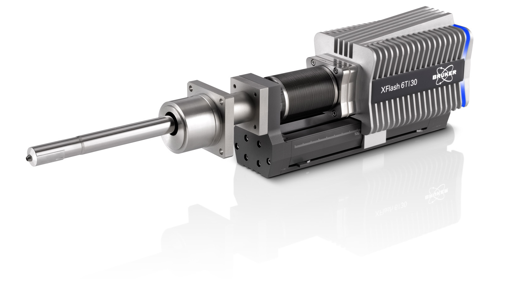
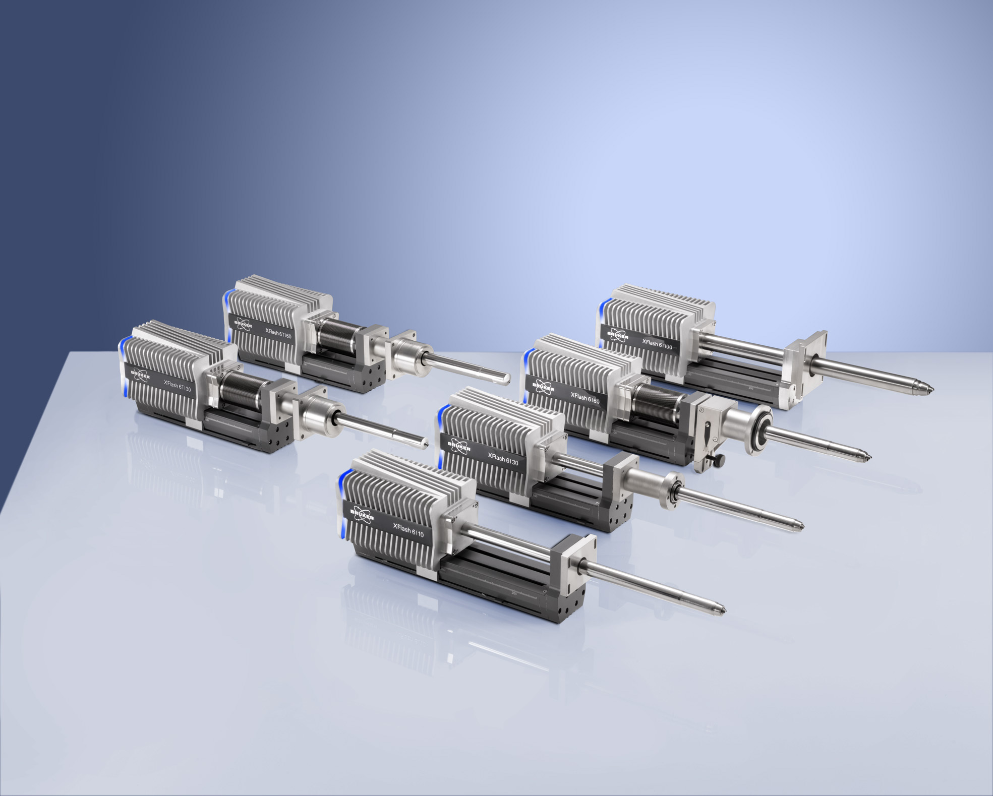
牛津仪器科技(上海)有限公司为您提供《闪存中分析NAND闪存检测方案(X射线能谱仪)》,该方案主要用于其他中分析NAND闪存检测,参考标准--,《闪存中分析NAND闪存检测方案(X射线能谱仪)》用到的仪器有牛津仪器Ultim Extreme无窗超级能谱、电镜专用微区成分分析---牛津仪器Ultim Max能谱仪
推荐专场
相关方案
更多
该厂商其他方案
更多