


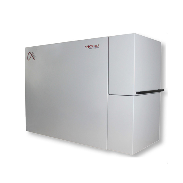
采用辉光放电光谱仪快速监测太阳能光伏电池中重要元素H、O、Cu、In、Ga、Se、Mo、Si、C、Ca、Zn、Cd、Te、Sn、Al等随深度的浓度变化,直观的分析太阳能光伏的镀层结构。辉光放电光谱仪的分析速度非常快,可快速反馈不同镀层加工条件对光伏性能的影响。非常适合工艺调整或质量监控。
方案详情

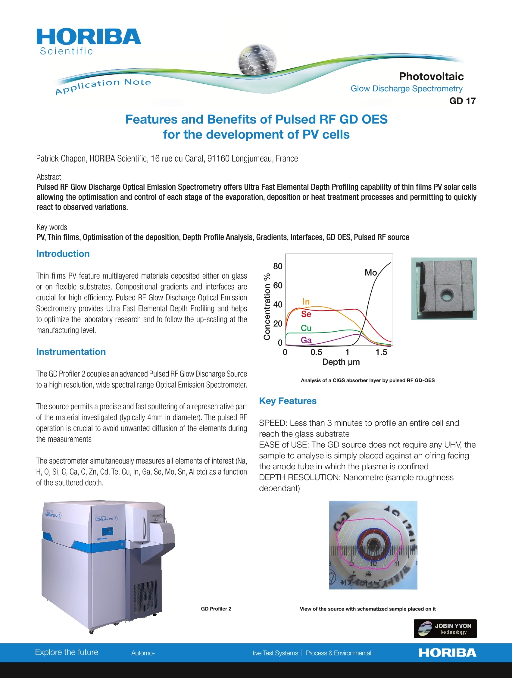
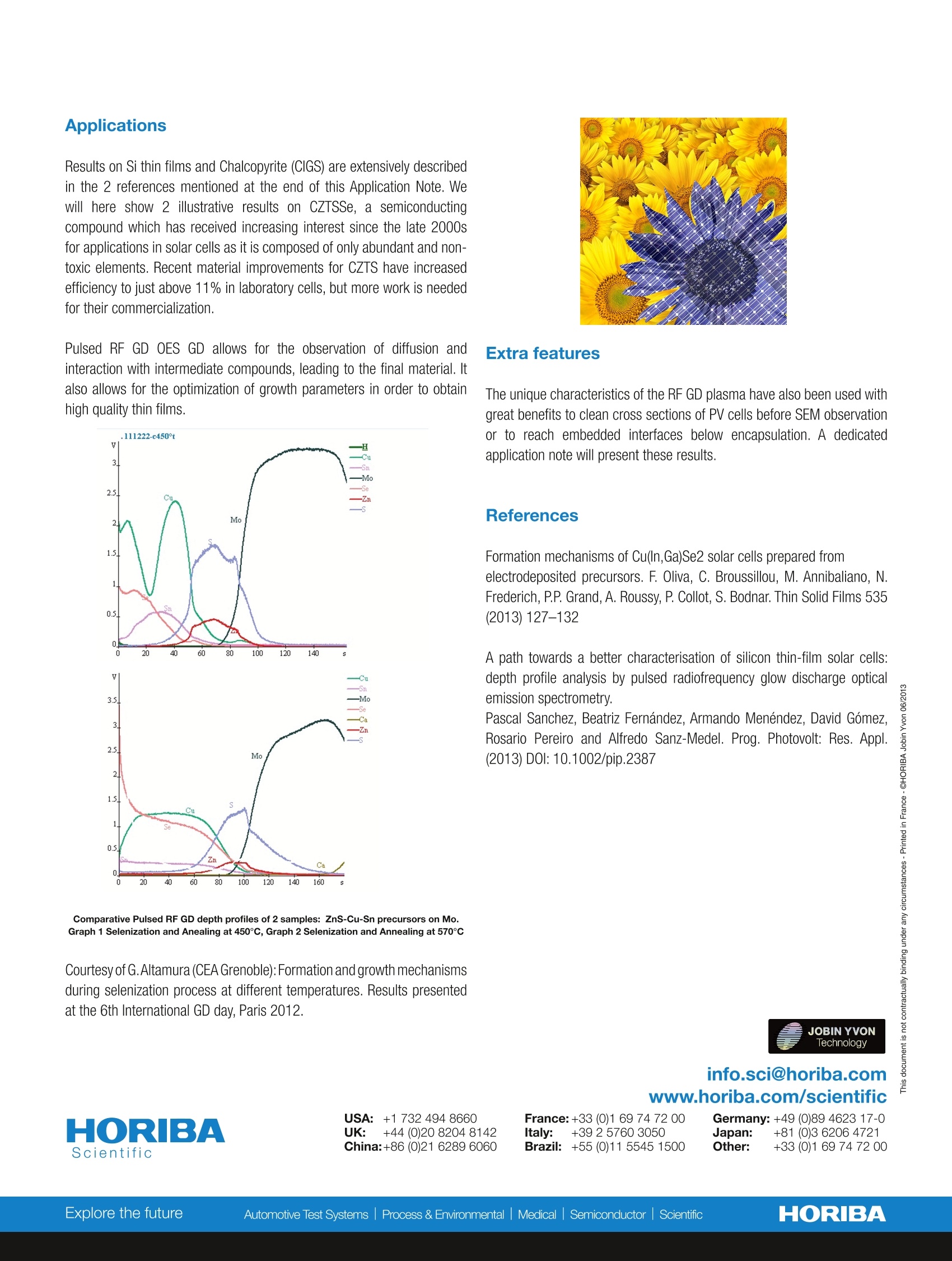
HORIBAScientificPhotovoltaicGD 17 Application Note Glow Discharge Spectrometry Features and Benefits of Pulsed RF GD OESfor the development of PV cells Patrick Chapon, HORIBA Scientific, 16 rue du Canal, 91160 Longjumeau,France Abstract Pulsed RF Glow Discharge Optical Emission Spectrometry offers Ultra Fast Elemental Depth Profiling capability of thin films PV solar cellsallowing the optimisation and control of each stage of the evaporation, deposition or heat treatment processes and permitting to quicklyreact to observed variations. Key words PV, Thin films, Optimisation of the deposition, Depth Profile Analysis, Gradients, Interfaces, GD OES, Pulsed RF source Introduction Thin films PV feature multilayered materials deposited either on glassor on flexible substrates. Compositional gradients and interfaces arecrucial for high efficiency. Pulsed RF Glow Discharge Optical EmissionSpectrometry provides Ultra Fast Elemental Depth Profiling and helpsto optimize the laboratory research and to follow the up-scaling at themanufacturing level. Instrumentation The GD Profiler 2 couples an advanced Pulsed RF Glow Discharge Sourceto a high resolution, wide spectral range Optical Emission Spectrometer The source permits a precise and fast sputtering of a representative partof the material investigated (typically 4mm in diameter). The pulsed RFoperation is crucial to avoid unwanted diffusion of the elements duringthe measurements The spectrometer simultaneously measures all elements of interest (Na,H, O, Si, C, Ca,C, Zn, Cd, Te, Cu, In, Ga, Se, Mo, Sn, Al etc) as a functionof the sputtered depth. Analysis of a CIGS absorber layer by pulsed RF GD-OES SPEED: Less than 3 minutes to profile an entire cell andreach the glass substrate EASE of USE: The GD source does not require any UHV, thesample to analyse is simply placed against an o’ring facingthe anode tube in which the plasma is confined DEPTH RESOLUTION: Nanometre (sample roughnessdependant) Results on Si thin films and Chalcopyrite (CIGS) are extensively describedin the 2 references mentioned at the end of this Application Note. Wewill here show2 illustrative results on CZTSSe, a semiconductingcompound which has received increasing interest since the late 2000sfor applications in solar cells as it is composed of only abundant and non-toxic elements. Recent material improvements for CZTS have increasedefficiency to just above 11% in laboratory cells, but more work is neededfor their commercialization. Pulsed RF GD OES GD allows for the observation of diffusion andinteraction with intermediate compounds, leading to the final material. Italso allows for the optimization of growth parameters in order to obtainhigh quality thin films. Comparative Pulsed RF GD depth profiles of 2 samples: ZnS-Cu-Sn precursors on Mo.Graph 1 Selenization and Anealing at 450°℃, Graph 2 Selenization and Annealing at 570°℃ Courtesy of G.Altamura (CEA Grenoble): Formation and growth mechanismsduring selenization process at different temperatures. Results presentedat the 6th International GD day, Paris 2012. USA::+1732 494 8660UK: +44 (0)20 8204 8142China:+86 (0)21 6289 6060 Extra features The unique characteristics of the RF GD plasma have also been used withgreat benefits to clean cross sections of PV cells before SEM observationor to reach embedded interfaces below encapsulation. A dedicatedapplication note will present these results. References Formation mechanisms of Cu(In,Ga)Se2 solar cells prepared fromelectrodeposited precursors. F. Oliva, C. Broussillou, M. Annibaliano, N.Frederich, P.P. Grand, A. Roussy, P. Collot,S. Bodnar. Thin Solid Films 535(2013) 127-132 A path towards a better characterisation of silicon thin-film solar cells:depth profile analysis by pulsed radiofrequency glow discharge opticalemission spectrometry. Pascal Sanchez, Beatriz Fernandez, Armando Menendez, David Gomez,Rosario Pereiro and Alfredo Sanz-Medel. Prog. Photovolt: Res. Appl.(2013) DOI: 10.1002/pip.2387 JOBIN YVON Technology info.sci@horiba.com www.horiba.com/scientific JOBIN YVONTechnologyHORIBAExplore the futureAutomo- tive Test Systems | Process & Environmental HORIBAExplore the futureAutomotive Test Systems| Process & Environmentalal|MedicalSemiconductorScientific
确定
还剩1页未读,是否继续阅读?

产品配置单

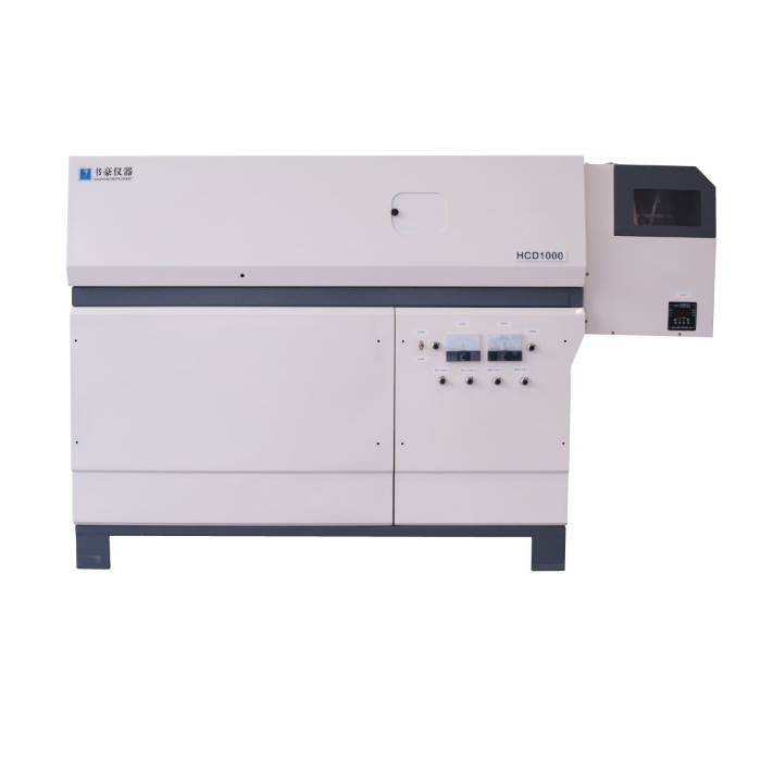
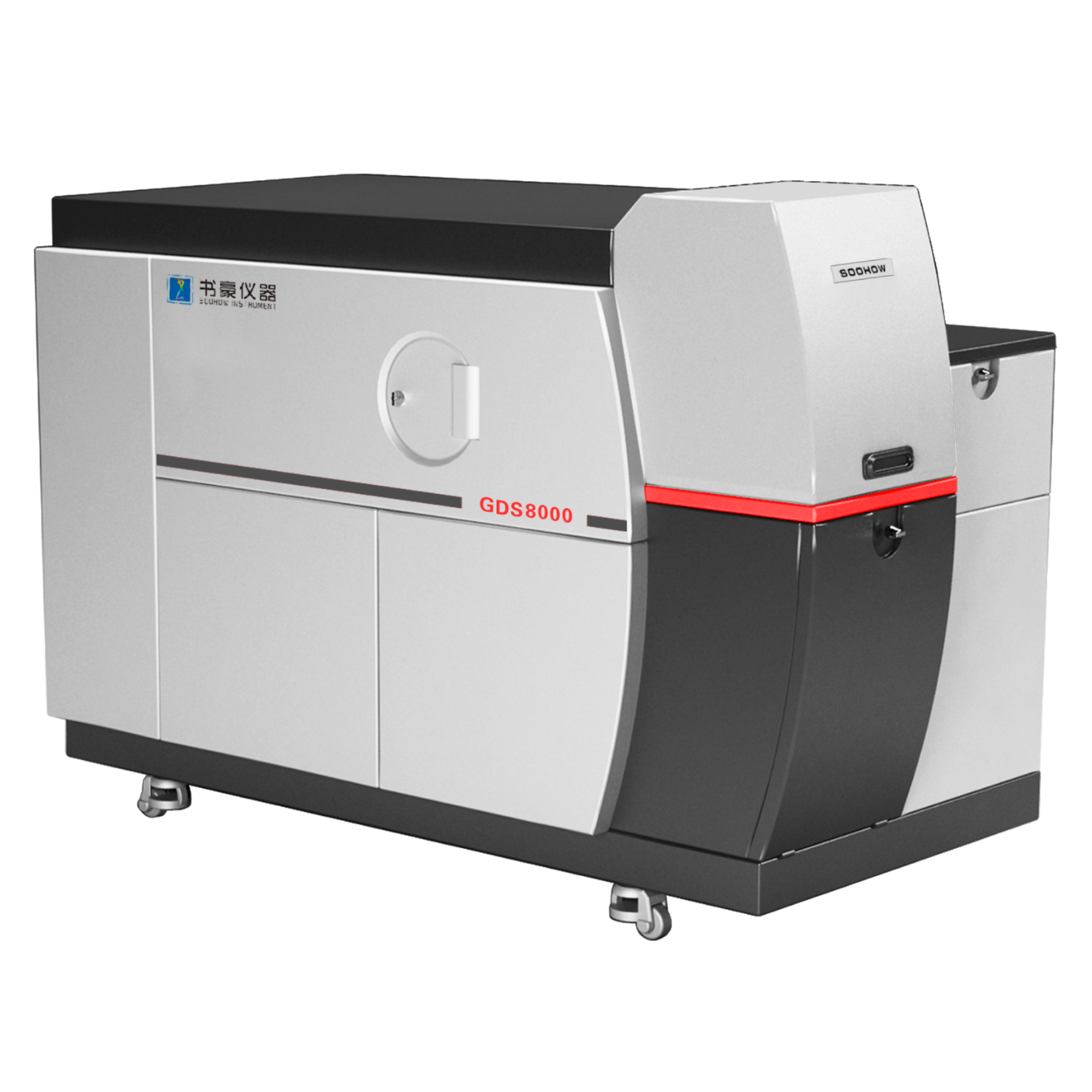
HORIBA(中国)为您提供《太阳能光伏电池的镀层结构表征》,该方案主要用于太阳能电池中--检测,参考标准--,《太阳能光伏电池的镀层结构表征》用到的仪器有HORIBA GD Profiler 2射频辉光放电光谱仪
推荐专场
相关方案
更多
该厂商其他方案
更多