


方案详情
文
人体血液中的铅( Pb )与严重的神经、行为和发育问题有关,在幼儿身上尤其如此。因此,欧盟通过了《限制有害物质指令》,禁止在电子产品中使用超过规定浓度的铅、镉、汞、铬( VI )、多溴联苯( PBB )和多溴联苯醚( PBDEs )。RoHS指令为电子设备和设备建立了1000ppm的Pb的最大允许浓度限值。 由于全球各地的制造商必须遵守其电子产品的有害物质限制规定,因此产品制造商及其供应链必须确定合适的分析仪器,以便对诸如铅等有害元素进行检测,因而灵敏度和准确度都很高。
目前,电感耦合等离子体光学和原子发射光谱(ICP-OES和ICP-AES)在业界被用作RoHS一致性验证的分析方法。 然而,ICP-OES需要在分析之前进行固体样品的复杂和耗时的酸溶解,以及重要的科学专业知识来执行分析。这使得ICP-OES不能作为一种快速的Pb监测技术,用于大量样品的质量控制。XRF近年来也用于监测成品中的铅。这种方法虽然方便,但其在为薄而小样品提供精确和精确的浓度测定方面面临着挑战。因此,XRF仅用于筛选RoHS元素,而不是用于最终确定元素含量。LIBS,LA-IC-PMS和ICP-OES在大多数样品上显示非常相似的结果
方案详情

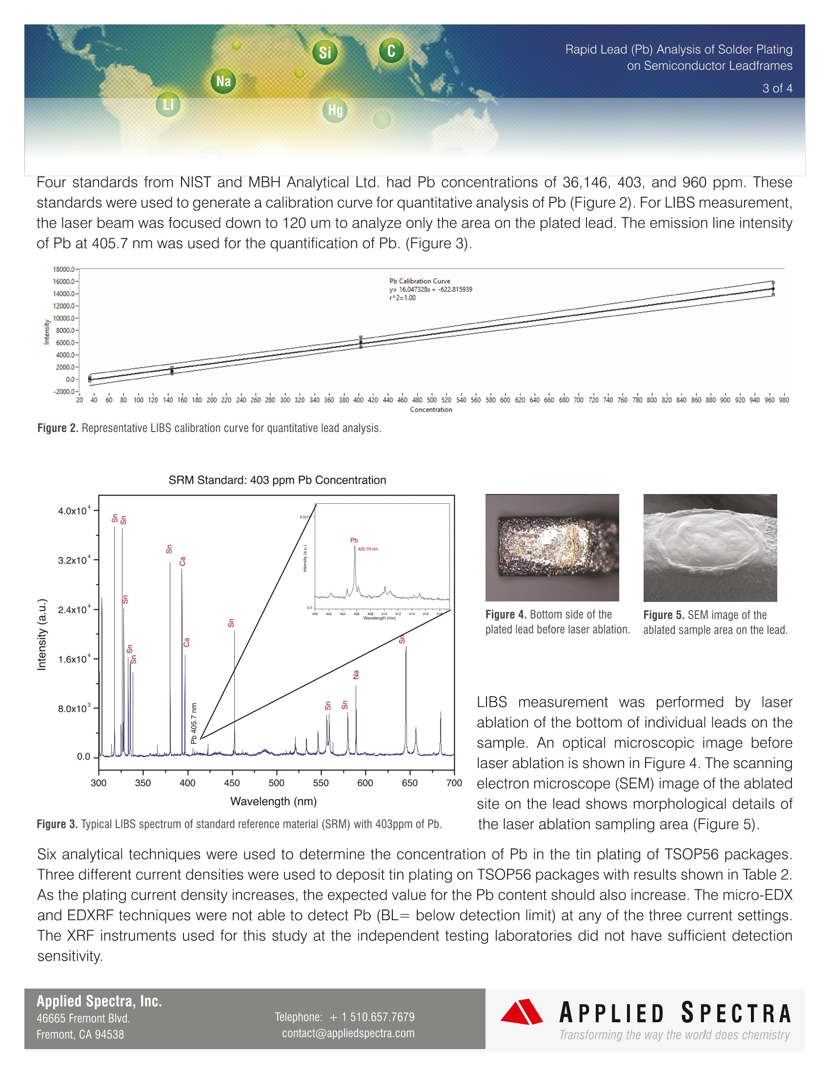
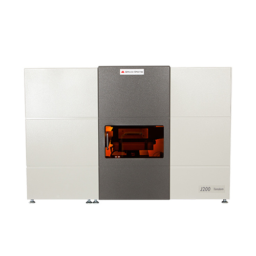
Pb Rapid Lead (Pb) Analysis of Thin Solder Platingon Semiconductor Leadframes Using LIBS Lead (Pb) in human blood has been associated withsevere neurological, behavioral and developmentalproblems, especially in young children. As a result, theEuropean Union passed the Restriction of HazardousSubstances Directive (RoHS) which bans the use ofPb, as well as Cd, Hg, Cr (VI), polybrominated biphenyl(PBBs) and polybrominated diphenyl ethers (PBDEs)above a specified concentration in electronic products. The RoHS directives establish a maximum allowableconcentration limit of Pb at 1000 ppm for electronicdevices and equipment. With manufacturers worldwidehaving to comply with hazardous substance restrictionsfor their electronic products, it is essential for the productmanufacturers and their supply chain to identify suitableanalytical instruments that are sensitive and accurate fortesting hazardous elements such as Pb. XRF techniques face challenges in providingaccurate and precise concentration determinationfor thin and small samples, such as tin solderplating for leadframe packages Currently, lInnductively Coupled Plasma-Optical andAtomic Emission Spectroscopy (ICP-OES and ICP-AES)are used in the industry as analytical methods for RoHScompliance verification. However, ICP-OES requirescomplex and time consuming acid dissolution of solidsamples prior to analysis, as well as significant scientificexpertise to perform the analysis. This makes ICP-OESunfit as a rapid Pb monitoring technique for applicationsrequiring high throughput of samples for quality control. XRF also has been used in recent years for monitoringPb in finished products. Although convenient, theXRF technique faces challenges in providing accurateandprecise concentration determination for thinand small samples, such as tin solder plating forleadframe packages. Consequently, XRF has beenused for screening RoHS elements, rather than for finaldetermination of the elemental content. LIBS (Laser Induced Breakdown Spectroscopy) is arapidly emerging analytical technology that usesafocused laser beam as the sample excitation source to perform sensitive elemental analysis even for small or thin samples. LIBS is ideal for the detection and measurementof toxic metals in small and thin electronic components, including those regulated by RoHS. This study demonstratedsensitive analysis of Pb content in thin solder plating of semiconductor leadframes by the J200 LIBS Instrument. Theperformance of the J200 LIBS Instrument was compared to five different methodologies commonly used to measurePb concentration in solder plating, namely: ·ICP-OES. ·Atomic Absorption (AA), · Energy Dispersive X-ray Fluorescence (EDXRF), ·micro-EDXRF, and · Laser Ablation-Inductively Coupled Plasma Mass Spectrometry (LA-ICPMS). Operating Parameters Applied Spectra Inc.'s J200 LIBS Instrument 1064 nm Nd:YAG laser (ns)and high performance ICCD detector(HP model) Applied Spectra Axiom Software FlexTM sample chamber ● Sample: Tin-plated semiconductor leadframe packages Quantitative analysis of Pb using Applied Spectra's Data Analysis Software Sample Analysis The samples used in this study were pure tin-plated, "thin small outline package”(TSOP56) products. These sampleswere divided into two groups: 1) tin plated TSOP56 packages at three different current densities, and 2) a group of 28leadframe packages produced without tin plating deposited on the leads, leaving the original bare copper substrateexposed. The last group acted as a control lot. Table 1 summarizes different currents applied to produce tin platingwith three Pb concentrations. Table 1. Summary of TSOP56 packages prepared with three different levels of Pb content of Snplating. No Pb Level Plating Current Total Quantity LOW Tin Plating at 50ASF 28 Strips 2 Regular Tin Plating at 140ASF 28 Strips 3 High Tin Plating at 200ASF 28 Strips 4 Copper bare frame No Tin Plating 28 Strips The samples were submitted to external, third-party laboratories for ICP-OES, AA, EDXRF,micro-EDXRF, and LA-ICP-MS analysis. LIBSanalysis was performed at Applied Spectra'sapplication laboratory in Fremont, CA using theJ200 LIBS Instrument. Laser and spectrometerparameters were optimized for the detection ofPb. Applied Spectra, Inc. Four standards from NIST and MBH Analytical Ltd. had Pb concentrations of 36,146, 403, and 960 ppm. Thesestandards were used to generate a calibration curve for quantitative analysis of Pb (Figure 2). For LIBS measurement,the laser beam was focused down to 120 um to analyze only the area on the plated lead. The emission line intensityof Pb at 405.7 nm was used for the quantification of Pb. (Figure 3). Figure 2. Representative LIBS calibration curve for quantitative lead analysis. Figure 4. Bottom side of theplated lead before laser ablation. Figure 5. SEM image of theablated sample area on the lead. Figure 3. Typical LIBS spectrum of standard reference material (SRM) with 403ppm of Pb. LIBS measurement was performed by laserablation of the bottom of individual leads on thesample. An optical microscopic image beforelaser ablation is shown in Figure 4. The scanningelectron microscope (SEM) image of the ablatedsite on the lead shows morphological details ofthe laser ablation sampling area (Figure 5). Six analytical techniques were used to determine the concentration of Pb in the tin plating of TSOP56 packages.Three different current densities were used to deposit tin plating on TSOP56 packages with results shown in Table 2.As the plating current density increases, the expected value for the Pb content should also increase. The micro-EDXand EDXRF techniques were not able to detect Pb (BL= below detection limit) at any of the three current settings.The XRF instruments used for this study at the independent testing laboratories did not have sufficient detectionsensitivity. ( Telephone: + 1510.657.7679contact@ap pl iedspectra.com ) LIBS, LA-IC-PMS and ICP-OES showed very similar results on most samples except that ICP-OES could not detectlead (ND= not detected) for the lowest plating current (50ASF) used. Table 2 also shows that Pbcontent was similarfor tin plating produced at medium- and high-current density, while it was lower for tin plating produced at the lowestcurrent setting. AAS showed a consistently lower Pb concentration at all plating currents. However, AAS detected Table 2. Comparison of Pb concentration (in ppm) determined by different analytical techniques for Sn plating ofTSOP5656 leadframe packages deposited at three different current settings. No Lead Level Plating Current PPM Level by Analysis Method AAS ICP-OES Micro-EDXRF EDXRF(5mm) LA-ICP-MS LIBS LOW Tin plating at 50ASF 12.2 ND ND BL 20 22 2 Regular Tin plating at 140ASF 18.7 40 ND BL 50 42 3 High Tin plating at 200ASF 29.3 43 ND BL 50 47 4 Copper bare frame (control lot) No tin plating 7.4 ND ND BL ND ND Legend: ND - Not Detected, BL - Below Detection Limits Figure 6. Pb concentration comparison between AAS, ICP-0ES, LA-ICP-MS, and LIBSfor Sn plated TSOP5656 leadframe packages at different currant setting. about 12 ppm of Pb in bare Cu substrates whileother techniques did not detect the presenceof Pb. This difference may have been due topotential contamination of samples or preparedsolutions. Figure 6 shows the summary of Pb concentrationresults from AAS, ICP-OES, LA-ICP-MS andLIBS. The results show close agreement of Pbconcentration values amon】g ILIBS, LA-ICP-MSand ICP-OES. Conclusion XRF-based techniques did not provide sufficient detection limits and the precision performance necessary toaccurately determine and monitor the Pb content of leadframe package products. AAS and ICP-OES are traditionaltechniques within the electronics industry,but due to extensive sample preparation time, they are unfit for fast, on-linemonitoring. LIBS analysis for Pb in leadframes produces results that correlate with data obtained from ICP-OES. In addition, LIBSprovides fast measurement times, together with the ability to monitor Pb content at various leadframe manufacturingsteps. High detection sensitivity for thin and tiny samples and direct solid analysis capability that eliminates toxicchemical waste make the J200 LIBS Instrument a powerful micro-analysis analytical tool for the electronic industry. ( Telephone : + 1510.657.7679contact@appliedspectra.com ) APPLIEDSPECTRAwww.AppliedSpectra.comTransforming the way the world does chemistry APPLIED SPECTRATransforming the way the world does chemistry LIBS,LA-IC-PMS和ICP-OES在大多数样品上显示非常相似的结果,除了ICP-OES无法检测所用最低电镀电流(50ASF)下的铅(ND =未检测到)含量。表2还显示,在中等和高电流密度下生产的锡镀层的铅含量相似,而在最低电流设置下生产的镀锡较低。AAS显示在所有电镀电流下铅浓度始终较低。然而,原子吸收光谱法在裸露的铜基底上检测到约12ppm的铅,而其他技术未检测到铅的存在。这种差异可能是由于样品或制备溶液潜在污染导致的。对细小样品的高检测灵敏度和消除有毒化学废物的直接固体分析能力,使J200 LIBS仪器成为电子工业中强有力的微分析分析工具。在三种不同电流设置下沉积的、TSOP5656引线框封装的锡镀层的不同分析技术测定的铅浓度(以ppm为单位)比较AAS,ICP-OES,LA-ICP-MS和LIBS之间的Pb浓度比较
确定


还剩2页未读,是否继续阅读?

产品配置单

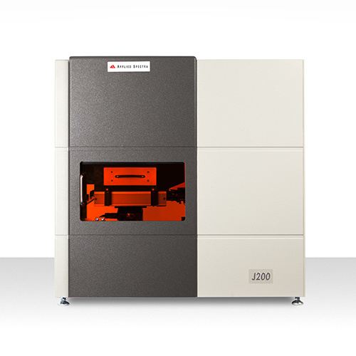
北京富尔邦科技发展有限责任公司为您提供《半导体引线框架镀层中铅检测方案(激光诱导击穿)》,该方案主要用于其他中铅检测,参考标准--,《半导体引线框架镀层中铅检测方案(激光诱导击穿)》用到的仪器有美国ASI 激光诱导击穿光谱仪(LIBS)
推荐专场
相关方案
更多