


方案详情
文
本文研究了在镀Mo膜钠钙玻璃(SLG)上共溅射和共蒸发工艺制备的CuIn1-xGaxSe2 (CIGS)吸收膜中主要和次要化学成分的LIBS光谱的影响。结果表明,共溅射技术制备的CIGS层的单脉冲剥烧蚀率高于共蒸发技术制备的CIGS层,从而导致各组分的LIBS信号强度较高。通过对辐照表面形貌和LIBS信号强度变化的研究,发现共溅射技术制备的CIGS薄膜存在元素分馏现象,而共蒸发技术制备的CIGS薄膜没有元素分馏现象。通过x射线衍射检测,证实了两种不同类型CIGS吸收膜的剥蚀和光谱特性的差异是导致其结晶性能差异的原因。此外,LIBS可以有效地测定从SLG扩散而来的CIGS薄膜中钠浓度的深度剖析。
方案详情

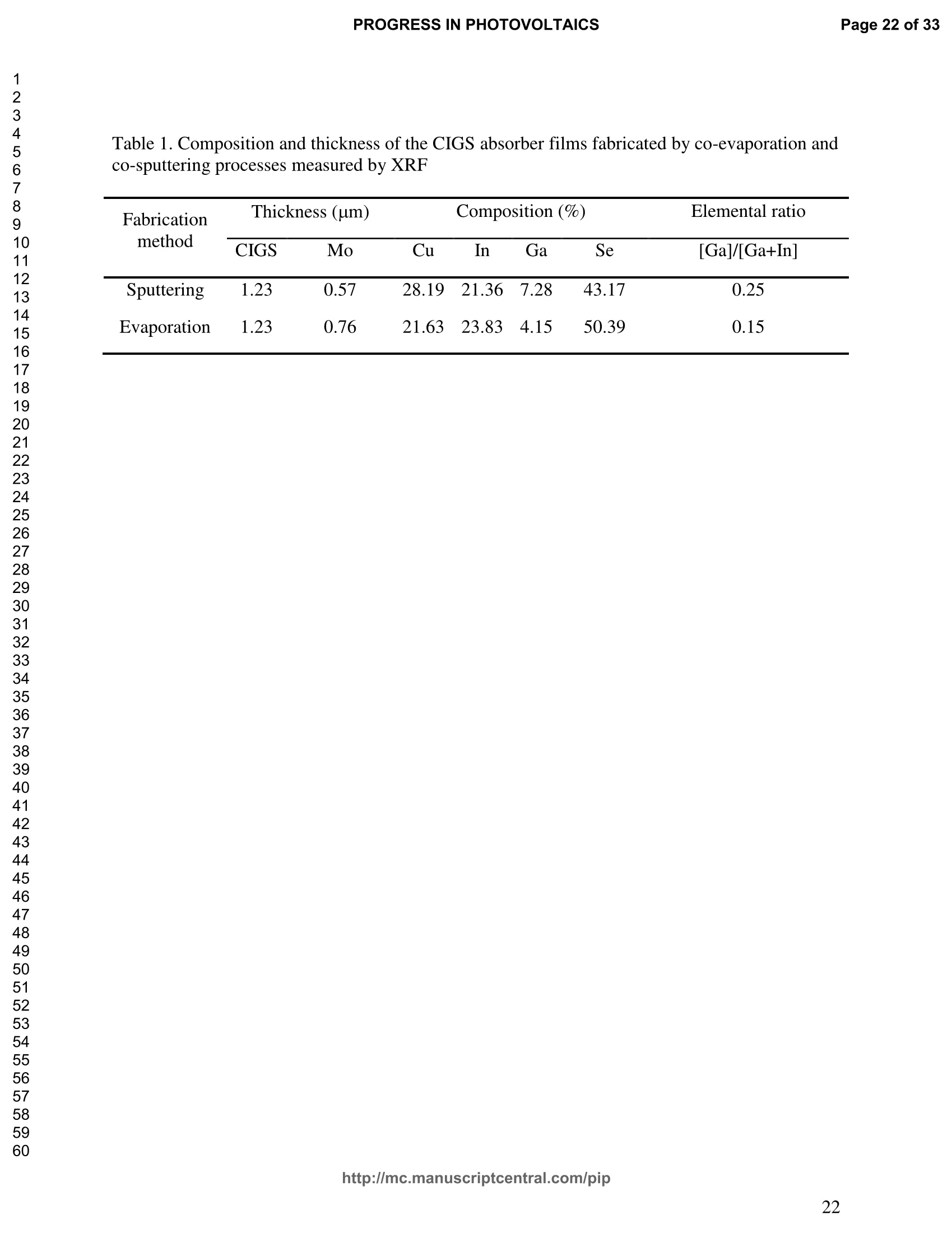
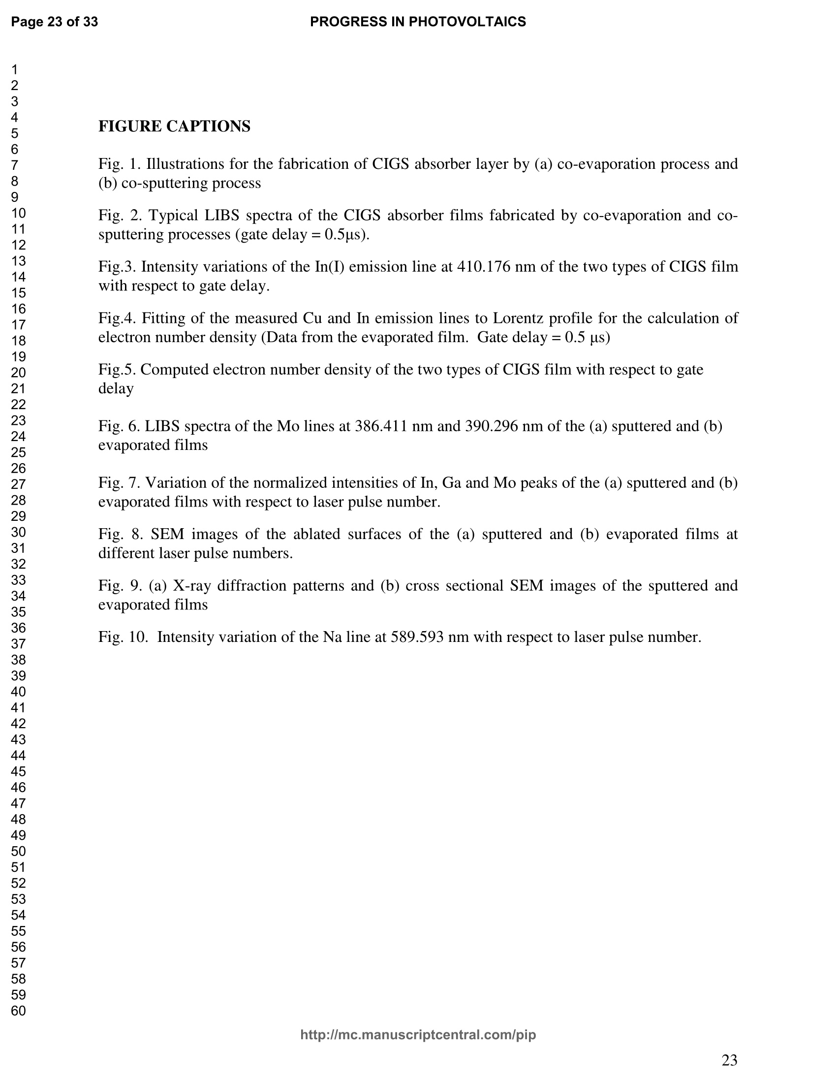
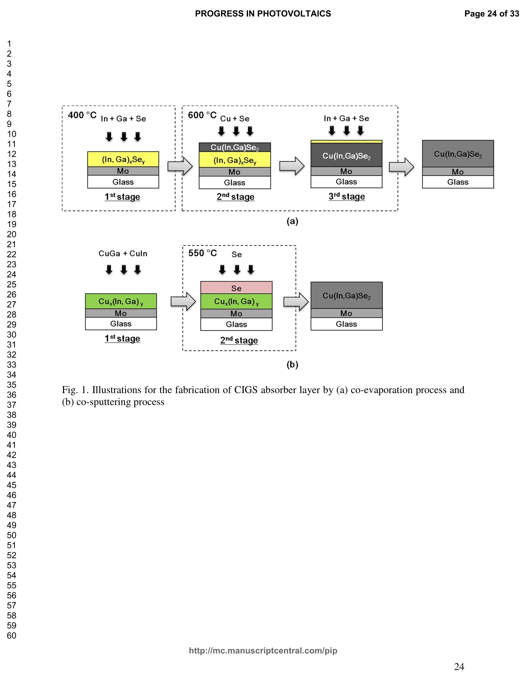
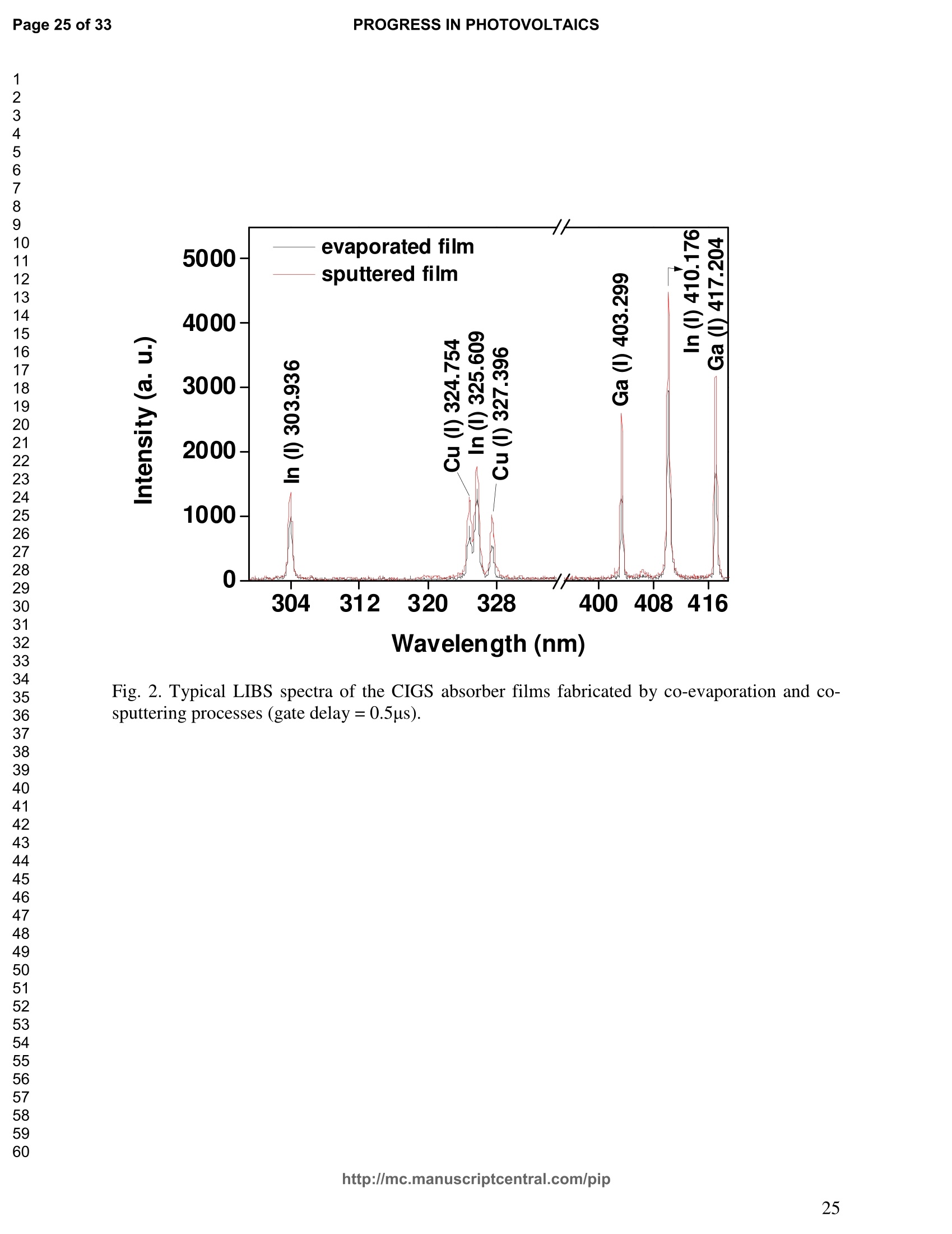
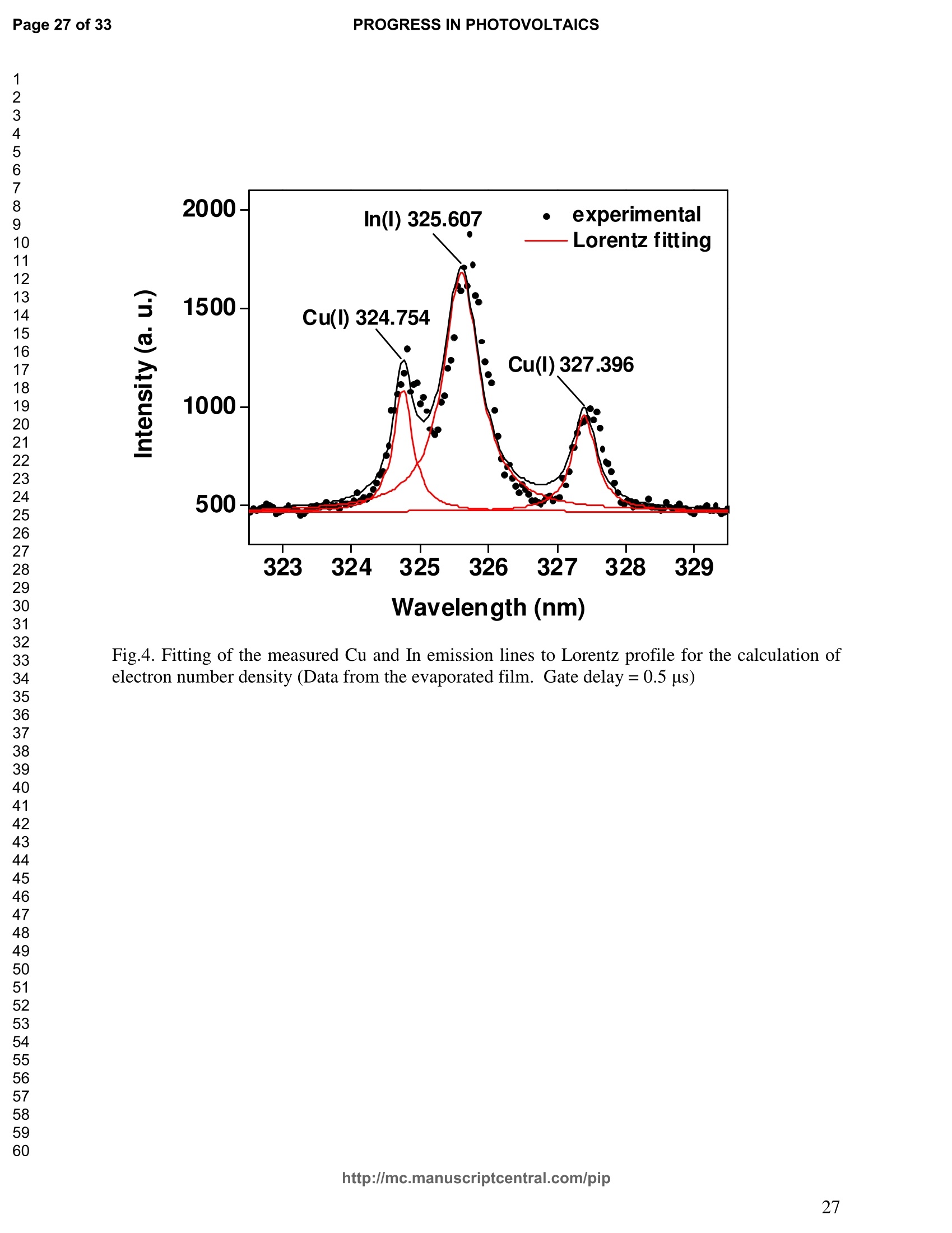
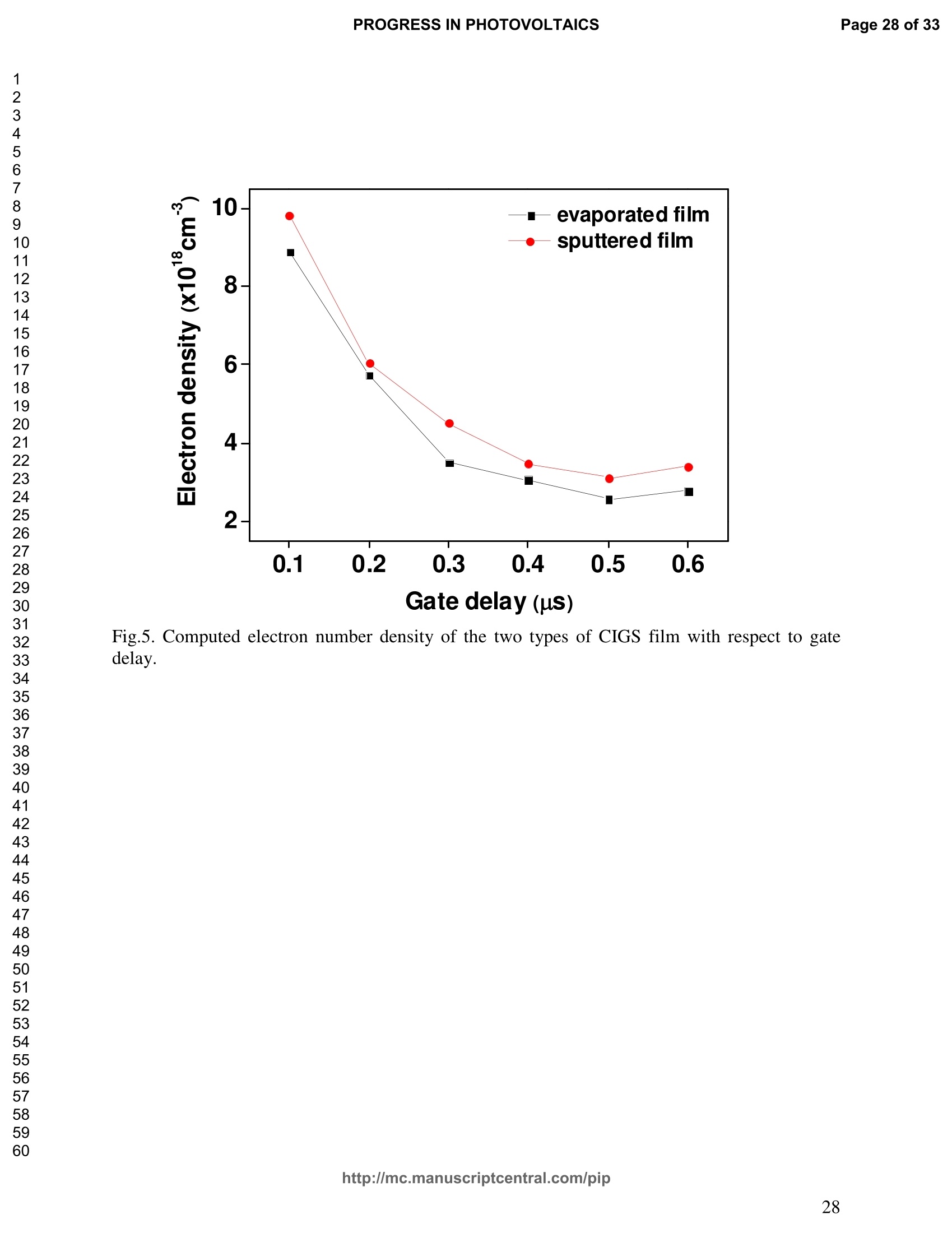
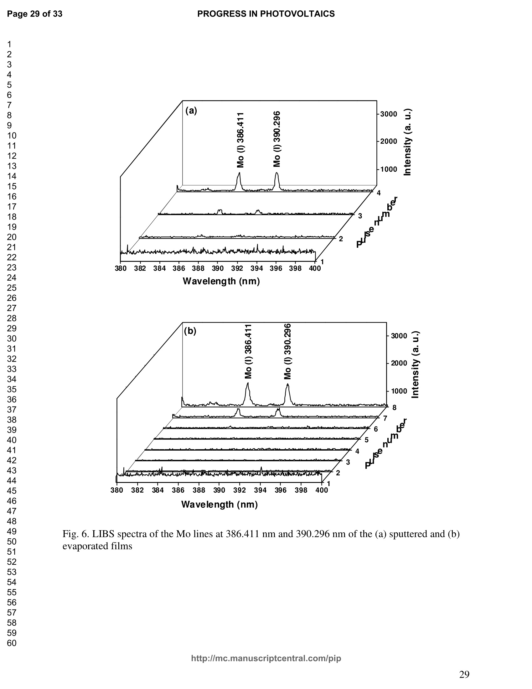
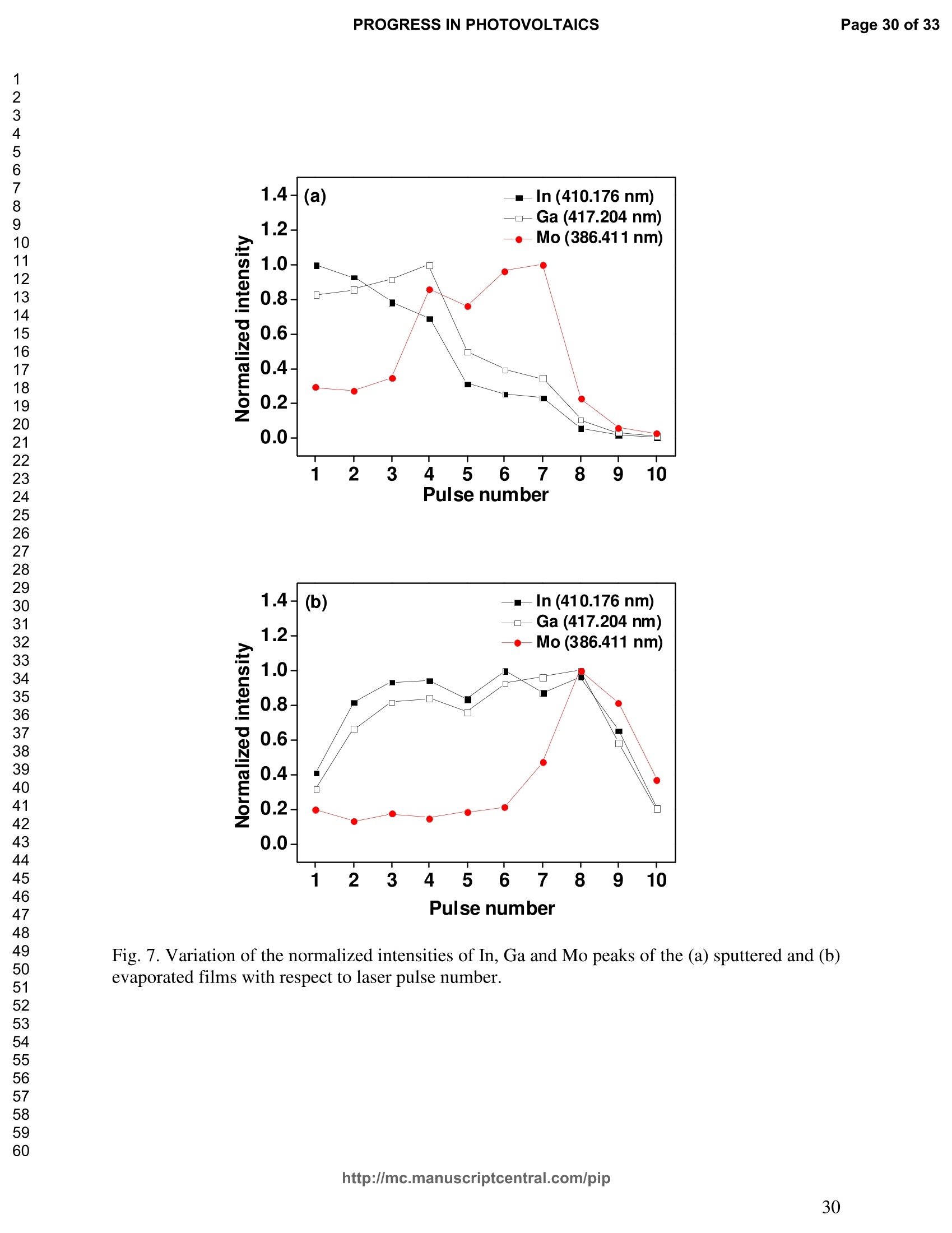
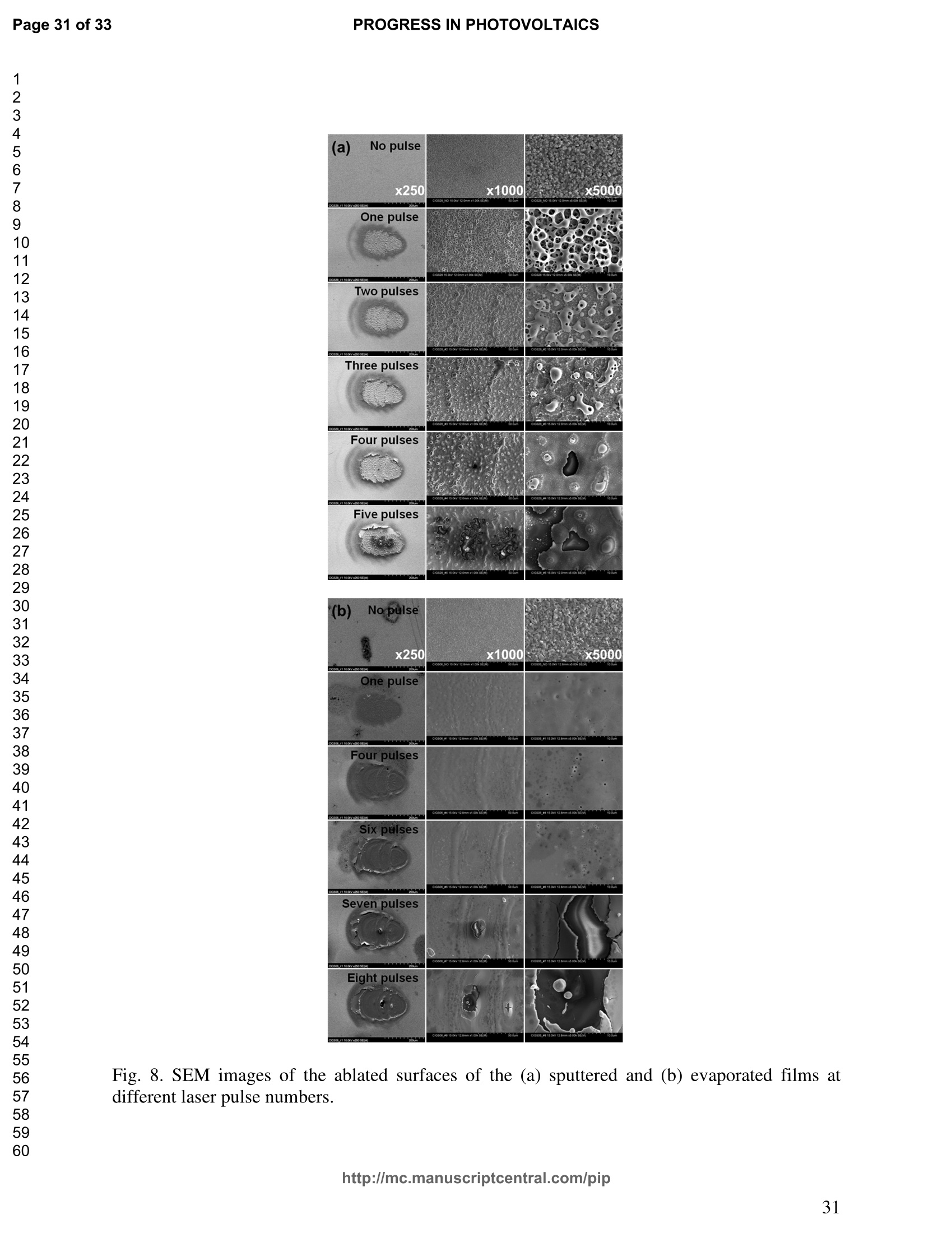
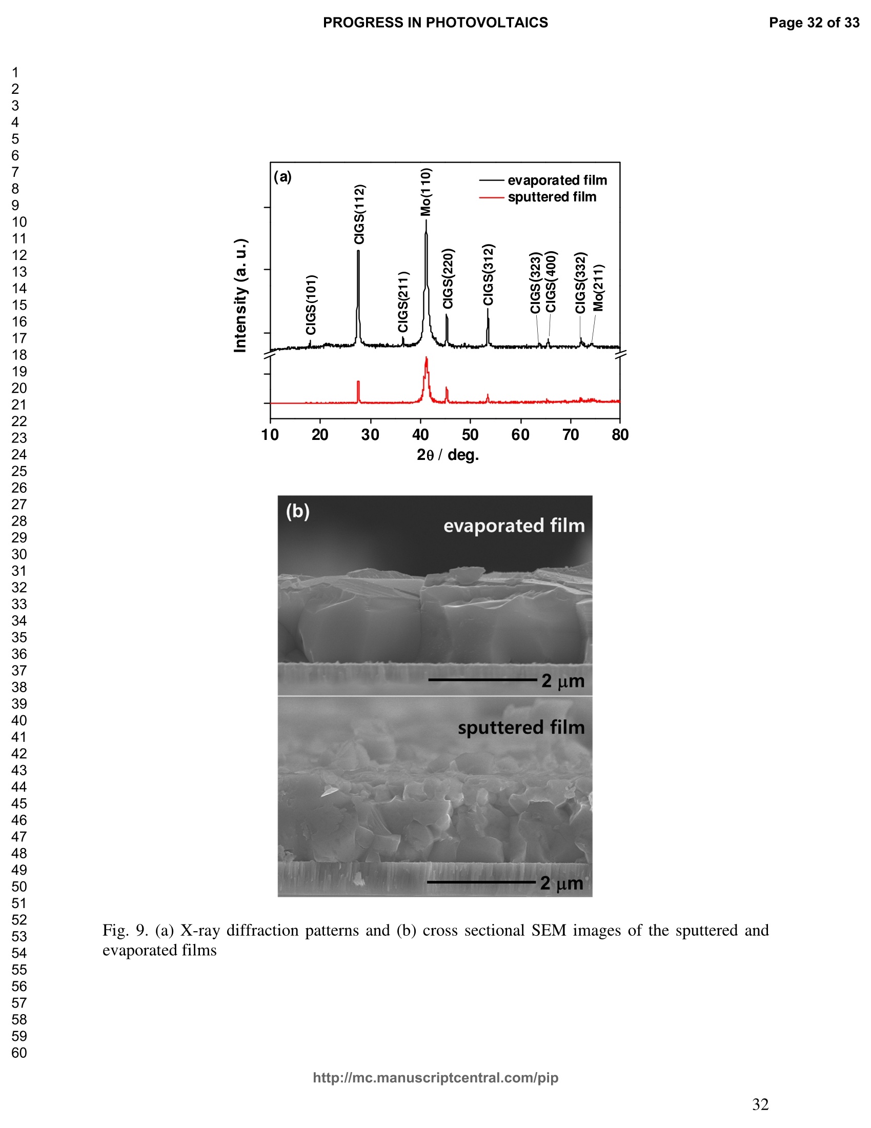
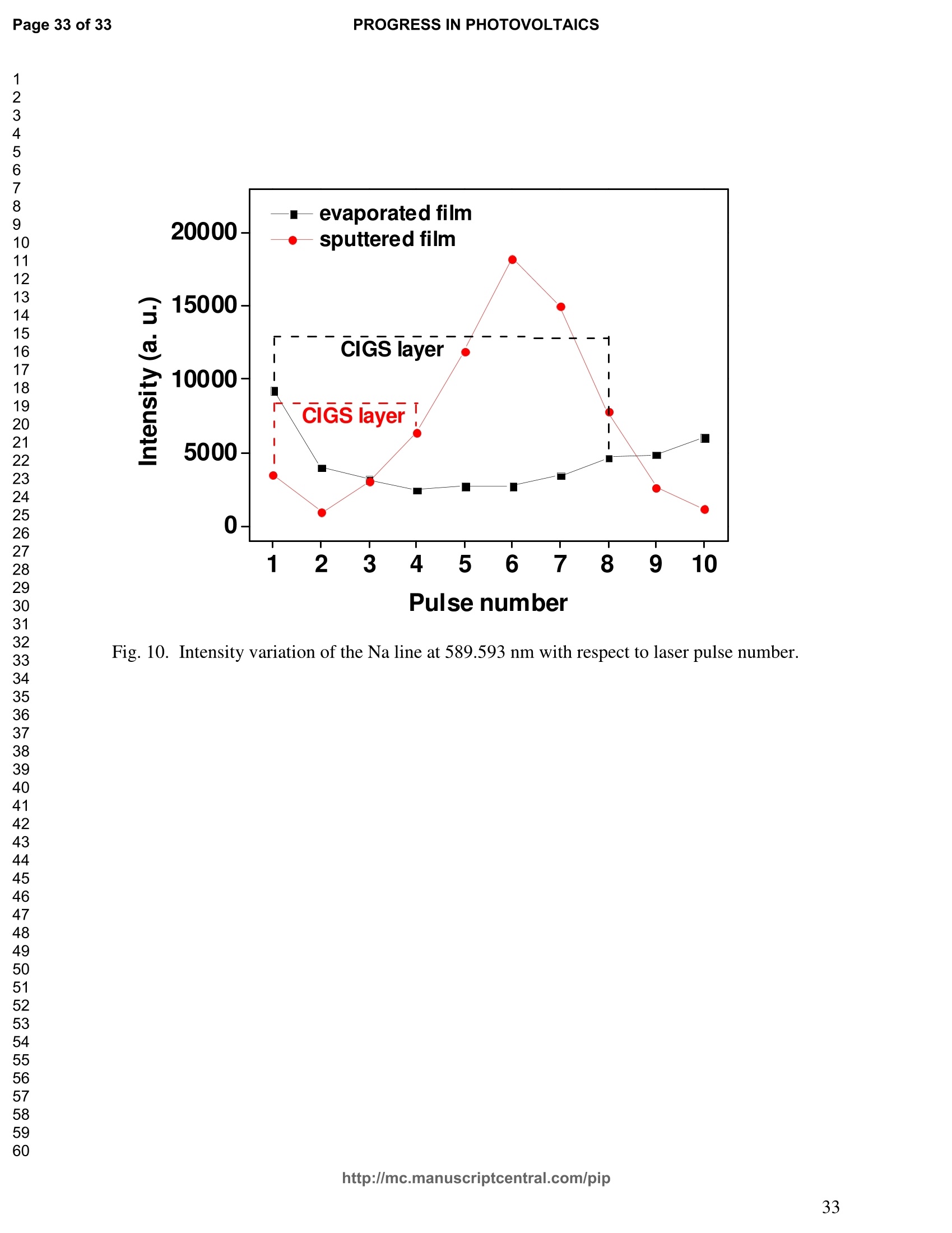
PROGRESS IN PHOTOVOLTAICS PROGRESS IN PHOTOVOLTAICSPage 1 of 33 Progress in Photovoltaics:Research and Applications Comparison of the ablation and spectroscopic characteristics of thin CuIn1-xGaxSe2 solar cell films fabricated by co-evaporation and co-sputtering processes Journal: Progress in Photovoltaics: Researchand Applications Manuscript ID: Draft Wiley- Manuscript type: Research Article Date Submitted by the Author: n/a Complete List of Authors: Lee, Seok; GIST, Kim, C. K.; GIST, Shim, H. S.; GIST, RISE Yoo, J. H.; Applied Spectra Inc., Russo, R. E.; LBNL, ; Applied Spectra Inc., Jeong, Sungho; Gwangju Institute of Science and Technology, School ofMechatronics Keywords: Solar cell, CIGS, Laser ablation, LIBS SCHOLARONE" Comparison of the ablation and spectroscopic characteristicsof thin CuIn1.xGaySe2 solar cell films fabricated by co-evaporation and co-sputtering processes s. H. Lee',C. K. Kim , H.S. Shim, J. H. Yoo’, R. E. Russo4and S. H. Jeongl,* School of Mechatronics, Gwangju Institute of Science and Technology, 1 Oryong-dong Buk-gu,Gwangju 500-712, Republic of Korea "Research Institute for Solar and Sustainable Energies, Gwangju Institute of Science andTechnology,1 Oryong-dong Buk-gu, Gwangju 500-712, Republic of Korea Applied Spectra Inc., 46661 Fremont Boulevard, Fremont, California 94538, USA“Lawrence Berkeley National Laboratory, 1 Cyclotron Road, Berkeley, California 94720, USA ABSTRACT The influence of fabrication processes on the LIBS (Laser Induced Breakdown Spectroscopy)spectra of major and minor chemical constituents in CuIn1-xGaxSe2 (CIGS) absorber filmsproduced by co-sputtering and co-evaporation techniques on Mo-coated soda lime glass (SLG)is reported. It was found that the ablation rate per pulse of CIGS layers fabricated by the co-sputtering technique is higher than those fabricated by the co-evaporation technique, resulting inhigher LIBSS sSi1gnal intensities of the constituent elements. The examination of surfacemorphology of irradiated surfaces and changes in LIBS signal intensities revealed evidences ofelemental fractionation for the CIGS films fabricated by co-sputtering technique but not for thoseby co-evaporation technique. From x-ray diffraction measurements, it was confirmed that thedifferences in the ablation and spectroscopic characteristics of the two different types of CIGS absorber films were contributed to the differences in crystalline properties. Furthermore, it wasdemonstrated that LIBS can effectively determine a depth profile of sodium concentration inCIGS thin films, diffused from SLG. KEYWORDS Solar cell, CIGS, Ablation, LIBS *Correspondence Sungho Jeong, School of Mechatronics, Gwangju Institute of Science and Technology, Gwangju500-712, Republic of Korea. E-mail: shjeong @gist.ac.kr 1. INTRODUCTION The second generation solar cells based on thin absorber layers such as amorphoussilicon (a-Si), CdTe, or CuIn1-xGaxSe2 (CIGS) have several advantages as compared to the firstgeneration solar cells based on crystalline silicon (c-Si). For example, thin film solar cells can bemanufactured at a lower cost than the c-Si counterparts [1]. Also, due to manufacturability onflexible substrates, thin film solar cells can be easily integrated into the roof or exterior walls of abuilding [2]. Accordingly, there have been tremendous research efforts to enhance the photo-conversion efficiency of thin film solar cells and to develop cost-effective manufacturingtechnologies. Among the various types of thin film solar cells, CIGS solar cells offer severalattractive properties for practical solar power applications such as high absorption coefficient andhigh photo-conversion efficiency of greater than 20% [3, 4]. The high absorption coefficient ofCIGS absorbing layer allows the effective film thickness to be in the range of only 1~2 microns,greatly reducing the material usage and associated costs compared to c-Si solar cells. The fabrication of thin CIGS absorbing layer can be achieved by various methods thatinclude sputtering [5-8], co-evaporation [9-11], electrodeposition [12], spray pyrolysis [13],paste coating [14] etc. Among these techniques, co-evaporation (shortly, evaporation) and co-sputtering(shortly,sputtering) processes are hepreferredmethods forrcommercialmanufacturing due to process scalability to mass production with consistent and high photo-conversion efficiency performance. In the evaporation process, the constituent elements (Cu, In,Ga, and Se) are simultaneously vaporized in a chamber and homogeneous CIGS thin film is thenformed by surface reaction on a substrate. The highest cell efficiency of 20.3 % has beenrecorded from the thin absorber film obtained by three-stage evaporation method [3]. In a two-step sputtering process, the Cu-In-Ga precursor thin films are deposited on the substrate from the metal targets of Cu, In, Ga or their alloys such as CuGa, CuIn, and In2Ses, and the CIGS filmsare obtained by subsequent reactionwith selenium source in the elevated temperatureenvironment.. The sputtering-based processes could be more adaptable for large area andcontinuous fabrication due to its simpler fabrication steps and the availability of existingmanufacturing facilities. Although many factors are known to influence on the efficiency of CIGS solar celldevices, the primary factor that requires most rigorous control is the elemental composition ofthe CIGS absorber layer. The stoichiometric ratio of main chemical constituents of the CIGSabsorber is known to govern its energetic and electronic properties [15-18]. Therefore, anaccurate measurement of the elemental composition of CIGS absorber layer is a crucial andchallenging issue for the fabrication process development and manufacturing of high efficiencyCIGS solar cells. Several analytical methods such as secondary ion mass spectrometry (SIMS)[19], inductively coupled plasma optical emission spectroscopy (ICP-OES) [20], glow dischargemass spectrometry (GDMS) [21], laser induced breakdown spectroscopy (LIBS) [22-23], or x-ray fluorescence (XRF) [3] have been applied for the elemental analysis of solar cells. Amongthese methods, however, only LIBSand XRF measurementsCanbee performed underatmospheric environment without the need for complex vacuum systems, thereby allowing in-situ monitoring and thus quality control compositional measurements during CIGS filmsmanufacturing. More commonly accepted technique such as ICP-OES requires extensive samplepreparation involving acid dissolution of bulk samples and the measurement takes too long for itto be an effective in-line method for production control. LIBS is a powerful method for elemental analysis in which real-time analysis, highsensitivity, and no sample preparation [24-32] are desired. LIBS has been successfully applied for environmental monitoring [33-35], biological species detection [36], military applications[37], precious artworks analysis [38], nuclear power station inspection [39], depth profiling ofthin film materials [40,41], etc. Recently, Darwiche et al. [22] reported the multi-elementalanalytical characterization of different qualities of solid silicon using LIBS, in particular, theinvestigation of optimal environmental parameters such as the pressure and the composition ofbuffering gas to improve detection limit of impurities such as boron, calcium and chromium etc.and addressed the application of LIBS for solar cell industry. Since LIBS only requires nano tomicro grams of mass for effective analysis, a thin film of 100 nm in thickness or less can beanalyzed by LIBS for elemental composition [41]. Consequently, LIBS could be the mosteffective technique for high-resolution elemental mapping and depth profiling analyses of thinCIGS layers. Furthermore, sodium (Na), one of the key elements governing the efficiency ofCIGS solar cells, can be measured with high detection sensitivity down to ppm level using LIBS.This provides LIBS a distinct advantage over XRF due to the XRF technique’s ineffectivenessfor lighter elements including Na. The short analysis time of LIBS, one second or less per singlelaser shot measurement [42], is another strong advantage for enabling rapid compositionalcharacterization and implementing real-time quality control in manufacturing lines. Despite theseclear advantages of LIBS, the applications of LIBS for elemental analysis of thin film solar cellmaterials has been hardly investigated and very limited number of research papers [43] havebeen published for LIBS analysis of CIGS absorber layer up to date. In this work, we report the results for LIBS analyses of CIGS thin absorber filmsfabricatedbysputteringg--acnd (evaporation-based rprocesses.The cdifferences inn aablationcharacteristics and LIBS signal intensity of the CIGS layers fabricated by these two differentdeposition methodsweree compared. IIn addition, their microstructural properties were investigated by x-ray diffraction (XRD) and scanning electron microscopy (SEM). It is shownthat the observed differences between the sputtered and evaporated films are associated withmicrostructural properties of the CIGS films. 2. EXPERIMENTAL SETUP The polycrystalline CIGS absorber films were grown by either a three-stage evaporationprocess or a two-step sputtering process as illustrated in Fig. 1. For substrate, soda-lime glass(SLG) (Abrisa Co.) coated with a Mo layer of below 1 um thickness was utilized. The Mo layerfunctions as the back electrode of a solar cell. For the fabrication of evaporated films, In, Ga andSe sources were first simultaneously evaporated at the substrate temperature of 400 °C to form a(In,Ga)2Ses layer with a thickness of 1 um, then as the second step Cu and Se were evaporatedand reacted with the (In,Ga)2Ses layer at the substrate temperature of 600 °℃ to form a Cu-richphase, and finally In, Ga and Se elements were again evaporated maintaining the same substratetemperature to produce a Cu-poor phase. For the sputtered films, a Cu-In-Ga precursor film wasfirst fabricated with the thickness of ca. 0.8 um by simultaneous sputtering of Cuo.6Gao.4 andCuo.5Ino.5 targets, and then the CIGS film was obtained by subsequent selenization reactionbetween precursor film and the Se source provided from a downstream Se cracker (JMON,Korea) at the substrate temperature of 550 C for 80 min. The differences in crystallographic characteristics of the CIGS thin films prepared byboth methods were investigated by XRD measurements (Rigaku X-ray diffractormeter with CuKo radiation). The chemical composition and thickness of both CIGS thin films were measuredby XRF using the CIGS calibration sample consisting of 18.4 at% Cu, 14.3 at% In, 5.0 at% Gaand 62.3 at% Se with the thickness of 2.15 um (F12H28F11-2,Calmetrics Inc.) as the reference, and the results are summarized in Table 1. The CIGS films appeared to have the same thicknessbutdifferenitt ccompositions.The: evaporatedfilmnwasfoundtoOtbea(Cu-poor ffilm(CuIni1Gao.19Se2.32), whereas the sputtered film resulted in a Se-poor phase (CuIn0.75Gao.25Se1.53). LIBS analyses of the two CIGS absorber films were carried out by using a commercialLIBS system (Applied Spectra Inc., Model:RT100-HP). The measurement system was equippedwith a high performance Czerny-Turner spectrometer that had a dual-grating turret providingmaximum spectral resolution of 0.1 nm with a 40 nm spectral window. A Q-switched Nd:YAGlaser ()=1064 nm,t=4ns) with a near top-hat spatial profile was used to generate plasma with afixed spot diameter of 150 um. For LIBS measurement, ten laser pulses were successively shot on the same spot of eachsample at the rate of 1 Hz and the evolution of LIBS spectra with respect to pulse number wasexamined. SEM (Hitach S-4700) images of the ablated surfaces at different pulse numbers weretaken to check the changes in surface morphology. 3.RESULTS AND DISCUSSION Fig. 2 shows the typical LIBS spectra of the two types of CIGS sample over the spectralranges of 298-338 and 395-418 nm, separated by a break line. The laser energy used for thesemeasurements was 0.48 mJ, corresponding to laser fluence of 2.72 J/cm , and the gate delay was0.55 us. These values of laser pulse energy and gate delay yielded the maximum signal tobackground ratio (SBR) and minimum full width at half maximum (FWHM) of the LIBSemission lines of analyzed chemical constituents. In general, the emission peak intensities of theconstituent elements reflect the original concentration of those elements within the target,although the relation between the ratio of actual concentration and the ratio of LIBS signal intensities needs to be further examined for precise calibration. Thus, the intensity ratios ofGa/(Ga+In) for both sputtered and evaporated CIGS films were calculated with Ga(I) peak at403.299 nm and In(I) peak at 410.176nm in Fig. 2 and compared. The calculated Ga/(Ga+In)intensity ratios of the sputtered and evaporated films were 0.33 and 0.28, respectively, implyingthat Ga concentration in the sputtered film is higher than that in the evaporated film. Similartrends were obtained when other Ga and In peaks in Fig. 2 were used for the same calculation.The relatively higher Ga concentration of the sputtered film than that of the evaporated filmpredicted by these LIBS spectra agrees with the XRF measurement results shown in Table1. While it is understood that the intensity ratios between elements revealed consistencywith the original composition, the intensities of emission lines for the sputtered CIGS filmappears significantly higher than those of the evaporated CIGS film over the entire spectral rangein Fig. 2. The higher emission lines’intensities of the sputtered film can be observed moreclearly for early gate delays as shown in Fig. 3 where the intensity differences of the In(I)emission line at 410.176 nm between the sputtered and evaporated films are shown. Note,however, that the In concentration measured by XRF in Table 1 showed a slightly lower valuefor the sputtered film. Since an enhanced peak intensity in LIBS spectra is a direct result ofincreased electron population in laser plasma [44], the observed relatively higher peak intensitiesof the sputtered film is considered to imply that a higher electron population was attained withinthe sputtered-film laser plasma. It is assumed that since both films were made of the sameconstituting elements, there exist no fundamental differences in the emission transitiorcharacteristics of those elements in both films. From the measured LIBS spectra, the electron number density of laser plasmas producedfrom the sputtered and evaporated films can be estimated as follows. First, it was assumed that the FWHM of the measured intensity peaks was determined mainly by the Stark effect andinstrumental characteristics. Then, the electron density could be found from the followingrelation [45], where AaStark is the Stark broadened FWHM, ne is the electron density, and Wref is the referencewidth for a reference electron density nee. Since the observed line width (AAobserved) iscontributed from both Stark effect and instrumental resolution (AAinstrumental),AAStark was obtainedby [46], The electron density ne was then calculated by Eq. (3) using the measured line width of Cuemission line at 324.754 nm and the known reference values of Wref= 0.0095 nm and ngref=0.66×10"’cmfor Cu [47]. To obtain △AStark, Cu in Eq. (4), AAobserved was extracted from the Lorentzfitting of the measured Cu peak (Fig.4) and AAinstrumental was replaced by the resolution of theICCD camera used in experiments (0.1 nm). The electron number densities calculated by usingEqs. (3) and (4) are shown in Fig. 5 as a function of gate delays. As shown in Fig. 5, the electrondensity of the sputtered film was calculated to be higher than that of the evaporated film for allgate delays, which reconfirms the observed higher intensity in Fig. 2. The higher spectral intensity in Fig. 2 and the higher computed electron number density inFig. 5 of the sputtered film are considered to confirm that a stronger atomization and ionizationhas taken place on the sputtered film. Since laser ablation conditions were identical for bothfilms, the observed higher emission line intensities of CIGS elements for the sputtered film wererelated to an enhanced ablation rate. To verify ablation rate difference between the sputtered and evaporated films, spectral changes of these films with respect to laser pulse number wereexamined. Specifically, the LIBS spectra of both samples were recorded as shown in Figs. 6(a)and 6(b), and the detection of Mo emission lines at 386.411 and 390.296 nm was used todetermine the point at which the laser ablation of Mo layer starts to occur. Note that thethicknesses of the two types of CIGS layers were the same at 1.23 um. The variation of In, Gaand Mo intensities, normalized by the maximum value obtained over the ten pulses, issummarized as a function of laser pulse number as shown in Fig. 7. In the case of sputtered film(Fig. 7 (a)), the intensity of Mo peak increased sharply at the 4" pulse, indicating that it took fourlaser pulses to remove the entire CIGS layer. Conversely, the intensities of Ga and In peaksdropped rapidly after the 4" shot. For the evaporated film, the increase of Mo peak intensity andthe drop of In and Ga intensities were observed at the 8h pulse (Fig. 7 (b)). The examination ofthe ablated surfaces of these two types of CIGS films revealed completely different ablation andcrater morphological characteristics as shown in Fig. 8. Note that the surfaces of both sampleshad similar structures prior to laser irradiation. First, the low magnification (x250) images of theablation craters in Figs. 8(a) and 8(b) show that the CIGS films were ablated nearly uniformlyover the entire laser spot for both samples until some uneven crater bottom profile emerge atincreased pulse numbers. After the first pulse, however, the surface of sputtered film starts todevelop a porous appearance (Fig. 8(a)), possibly due to fractional ablation of the differentconstituent elements. With increasing pulse number, the porous look of the surface becomes lessapparent because of the melting and subsequent re-solidification of the ablated surface. At the 4"shot, the CIGS layer was ruptured in the middle revealing the underlying layer (Mo), whichmarked the sharp increase of Mo signal intensity at the 4h pulse in Fig. 7(a). Note that the Galine intensity of the sputtered film in Fig. 7(a) increased until the 4" laser pulse, whereas that of In peak showed a continuous decrease, which can be an indication of preferential vaporization ofthe different constituent elements. If LIBS analysis is performed with an assumption that peakintensity is proportional to the original composition of the sample, the elemental fractionation,possibly observed for the sputtered film could become the source of measurement errors for theelemental composition of CIGS layers. On the other hand, the evaporated film showed acompletely different surface morphology after the 1 shot, that is, a uniform melting of thesurface with no porosity (Fig. 8(b)). The surface morphology of the evaporated film remainedalmost the same for increasing pulse numbers until a rupture took place in the middle at theseventh shot which also marked the sudden increase of Mo signal intensity in Fig. 7(b). Theobserved consistency in the morphology of the ablated surface for the evaporated film by thelaser pulse number 2 through 6 may be an indication of mass removal with reduced elementalfractionation, and have led to more consistent intensity ratio of Ga and In peaks in Fig. 7(b).These results imply that more accurate estimation of elemental concentration could be achievedby just considering LIBS intensity measurements alone for the evaporated film. It is known that the fractional ablation can occur due to different alloy structure ofcomposites even for the same element [48]. The observed differences in LIBS spectra andablation morphologies between the sputtered and evaporated films were understood to be closelyrelated to micro-structural differences of the CIGS layers fabricated by thetwo methods. For theverification of structural differences, XRD measurements were carried out and the results areshown in Fig. 9(a). The peaks related to a CIGS crystal are observed at 17.9,27.6, 36.5, 45.2,53.4, 63.7, 65.4, and 72.2, which represent (101), (112),(211),(220),(312),(323), (400) and(332) crystal planes for a chalcopyrite structures, respectively (JCPDS 86-1503) [49]. The XRDpatterns revealed the existence of tetragonal chalcopyrite crystal structure for both samples, which was confirmed by the main peaks appeared at (112), (220),(312), (400) and (332) planesof the chalcopyrite structure [50, 51]. However, the (101) and (323) peaks are absent in thesputtered film data. In general, relatively stronger peak intensities were observed for theevaporated film over the characteristic peaks, implying higher crystalline properties of theevaporated film than the sputtered film. The crystalline characteristics of the sputtered andevaporated films were also examined with cross-sectional SEM images as shown in Fig. 9(b),which clearly show that large crystal grains were produced in the evaporated film, whereas thesputtered film yielded small, rounded, granular microstructure with poorly defined grain size.The observed large number of grain boundaries in the sputtered film is considered to havecontributed to a relatively stronger absorption of the incident laser energy. Note that impurity isanother factor that is closely related to laser energy absorption but little impurity signals wereobserved in the LIBS data of both films. These results from XRD and SEM measurementsdemonstrate that the crystalline properties of the CIGS absorber layers vary with fabricationprocesses, which in turn results in the differences in spectroscopic characteristics during LIBSelemental analysis of these layers. Finally, it is shown that Na profile along the depth of CIGS layers due to diffusion fromthe SLG substrate during fabrication process can be determined by LIBS. Na content in the CIGSlayer is one of the crucial factors governing solar cell efficiency [53]. For the measurement of Nacontent, the intensity variation of Na line at 589.593nm was examined with varying laser pulsenumbers as shown in Fig. 10. Based on the data in Fig. 7, the laser pulses up to the 4h shot and8"shot for the sputtered and evaporated films, respectively, were considered for the Na profileexamination. For both samples, it is observed that the Na concentration near the surface and nearthe CIGS-Mo interface was higher than that in the bulk area, which agrees with the previous study that reported a high Na content in the surface regime and a nearly uniform distribution inthe bulk [52, 53]. These results demonstrate the potential for in-situ depth profiling of CIGSlayers with LIBS. 4. CONCLUSION In this work, LIBS elemental analysis of the absorber layer of CIGS solar cells fabricatedby two different methods, co-sputtering and co-evaporation processes, was carried out in orderto investigate how the fabrication process influences on the LIBS spectra. It was found that theLIBS intensity of the constituent elements of the sputtered film is significantly higher than thatof the evaporated film of similar composition and the same thickness. On the contrary, thesputtered film revealed evidences of possible preferential vaporization of different elements thatmust be accounted for accurate estimation of elemental composition by LIBS. On the other hand,the evaporated film showed a high consistency in the individual line intensities. The observeddifferences in LIBS signal characteristics between the CIGS films fabricated by two differenttypes of technique were found to originate from the fundamental differences in crystallineproperties of the CIGS layers produced by the two methods. These results confirm that thecritical parameters for LIBS elemental analysis of CIGS solar cells should include the fabricationprocess and resulting material characteristics. ACKNOWLEDGMENT This work was supported by the National Research Foundation of Korea (NRF) grant funded bythe Korea government (MEST) (No. 2011-0029850). ( REFERENCES ) [1] Chopra KL, Paulson PD, Dutta V. Thin-film solar cells: an overview. ProgressinPhotovoltaics: Research and Applications 2004; 12:69-92. [2] Pagliaro M, Ciriminna R, Palmisano G. Flexible solar cells. ChemSusChem 2008; 1: 880-891. [3] Jackson P, Hariskos D, Lotter E, Paetel S, Wuerz R, Menner R, Wischmann W, Powalla M.New world record efficiency for Cu(In,Ga)Se2 thin-film solar cells beyond 20%. Progress inPhotovoltaics: Research and Applications 2011; 19: 894-897. [4] Green MA, Emery K, Hishikawa Y, Warta W. Solar cell efficiency tables (version 37).Progress in Photovoltaics: Research and Applications 2011;19:84-92. [5] Marudachalam M, Birkmire RW, Hichri H, Schultz JM, Swartzlander A, Al-Jassim MM.Phases, morphology, and diffusion in CuInxGa1-xSe2 thin films. Journal Applied Physics1997; 82:2896-2905. [6] Kushiya K, Ohshita M, Hara I, Tanaka Y, Sang B, Nagoya Y, Tachiyuki M, Yamase O.Yield issues on the fabrication of 30 cmx30 cm-sized Cu(In,Ga)Se-based thin-filmmodules. Solar Energy Materials and Solar Cells 2003; 75: 171-178. [7] Nishiwaki S, Satoh T, Hashimoto Y, Negami T, Wada T. Preparation of Cu(In,Ga)Sez thinfilms at low substrate temperatures.Journal of Materials Research 2001;16:394-399. [8] Dimmler B, Dittrich H, Schock HW. Structure and morphology of evaporated bilayer andselenized CuInSe films. Proceedings of the 20t1h IEEE Photovoltaic Solar Energy Conference, Las Vegas, 1988; 1426-1430. [9] Tuttle JR, ContrerasM,, Tennant A, Albin D, Noufi R. High efficiency thin-filmCu(In,Ga)Sez-based photovoltaic devices: progress towards a universal approach to absorberformation. Proceedings of the 23rd IEEE Photovoltaic Specialists Conference, New York,1993;415-421. [10]Gabor AM, Tuttle JR, Albin DS, Contreras MA, Noufi R, Hermann AM. High-efficiencyCuInxGa1-xSe2 solar cells made from (Inx,Ga1-x)2Ses precursor films. Applied PhysicsLetters 1994; 65: 198-200. [11]Zweigart S, Walter Th, Koble Ch, Sun SM, Ruhle U, Schock HW. Sequential deposition ofCu(In,Ga)(S,Se)2,”Proceedings of the lst IEEE World Conference on Photovoltaic EnergyConversion, Hawaii, 1994; 60-67. [12]Hodes G, Lokhande CD, Cahen D. The flexibility of electrodeposition for preparation ofCuInS(Se)2 films. Journal of Electrochemistry Society 1986; 133: C113. [13]Krunks M, Kijatkina O, Rebane H, Oja I, Mikli V, Mere A. Composition of CuInS2 thinfilms prepared by spray pyrolysis. Thin Solid Films 2002; 403-404:71-75. [14]Kaelin M, Rudmann D, Kurdesau F, Zogg H, Meyer T, Tiwari AN. Low-cost CIGS solarcells by paste coating and selenization. Thin Solid Films 2005; 480-481: 486-490. [15]Mudryi AV, Gremenok VF, Karotki AV, Zalesski VB, Yakushev MV, Luckert F, Martin R.Structural and optical properties of thin films of Cu(In,Ga)Se semiconductor compounds.Journal of Applied Spectroscopy 2010; 77:371-377. [16]Wei SH, Zhang SB, Zunger A. Effects of Ga addition to CuInSe2 on its electronic, structural,and defect properties. Applied Physics Letters 1998; 72:3199-3201. [17]Dullweber T, Hanna G, Shams-Kolahi W, Schwartzlander A, Contreras MA, Noufi F,Schock HW. Study of the effect of gallium grading in Cu(In,Ga)Se. Thin Solid Films 2000;361-362:478-481. [18]Ishizuka S, Yamada A, Matsubara K, Fons P, Sakurai K, Niki S. Alkali incorporationcontrol in Cu(In,Ga)Se thin films using silicate thin layers and applications in enhancingflexible solar cell efficiency. Applied Physics Letters 2008; 93: 124105. [19]Durose K, Asher SE, Jaegermann W, Levi D, McCandless BE, Metzger W, Moutinho H,Paulson PD, Perkins CL. Sites JR, Teeter G, Terheggen M. Physical Characterization ofThin-film Solar Cells. Progress in Photovoltaics: Research and Applications 2004; 12: 177-217. [20]Martinuzzi S, Perichaud I, Trassy C, Degoulange J. n-Type Multicrystalline Silicon WafersPrepared from Plasma Torch Refined Upgraded Metallurgical Feedstock. Progress inPhotovoltaics: Research and Applications 2009; 17: 297-305. [21]Modanese C, Sabatino MD, Spiland AK, Peter K, Arnberg L. Investigation of bulk and solarcell properties of ingots cast from compensated solar grade silicon. Progress inPhotovoltaics: Research and Applications 2011; 19: 45-53. [22]Darwiche S, Benmansour M, Eliezer N, Morvan D. Laser-induced breakdown spectroscopyfor photovoltaic silicon wafer analysis. Progress in Photovoltaics: Research andApplications 2011;DOI:10.1002/pip.1209. [23]Hidalgo M, Martin F, Laserna JJ. Laser-induced breakdown spectrometry of titaniumDioxide Antireflection Coatings in Photovoltaic Cells. Analytical Chemistry 1996; 68:1095-1100. [24]Radziemski LJ. From laser to LIBS, the path of technology development. SpectrochimicaActa Part B 2002; 57:1109-1113. [25]Sneddon J, Lee YI. Novel and recent applications of elemental determination by laser-induced breakdown spectrometry. Analytical Letters 1999; 32: 2143-2162. [26]Song K, Lee YI, Sneddon J. Recent developments in instrumentation for laser inducedbreakdown spectroscopy. Applied Spectroscopy Reviews 2002;37:89-117. [27]Cremers DA, Radzimski LJ. Handbook of Laser-Induced Breakdown Spectroscopy.JohnWiley & Sons: England, 2006; 302. [28]Miziolek A, PalleschiV, Schechter I.Laser-Induced Breakdown Spectroscopy (LIBS):Fundamentals and Applications. Cambridge University Press., United Kingdom, Cambridge,2006;638. [29]Russo R, Mao X, Liu H, Gonzalez J, Mao S. Laser ablation in analytical chemistry-a review.Talanta2002;57:425-451. [30]Tognoni E, Palleschi V, Corsi M, Cristoforetti G. Quantitative micro-analysis by laser-induced breakdown spectroscopy: a review of the experimental approaches. SpectrochimicaActa Part B 2002;57:1115-1130. [31]Fichet P, Menut D, Brennetot R, Vors E, Rivoallan A. Analysis by laser-induced breakdownspectroscopy of complex solids, liquids, and powders with an echelle spectrometer. AppliedOptics 2003; 42:6029-6035. [32]Vadillo J, Laserna J. Laser-induced plasma spectrometry: truly a surface analytical tool.Spectrochimica Acta Part B 2004; 59:147-161. [33]Dudragne L, Adam Ph, Amouroux J. Time-resolved laser-induced breakdown spectroscopy:application for qualitative and quantitative detection of fluorine, chlorine, sulfur, and carbonin air. Applied Spectroscopy 1998; 52: 1321-1327. [34]Zhang H, Yueh F, Singh J. Laser-induced breakdown spectrometryasa multimetalcontinuous-emission monitor. Applied Optics 1999; 38: 1459-1466. [35]Hahn D. Laser-induced breakdown spectroscopy for sizing and elemental analysis ofdiscrete aerosol particles. Applied Physics Letters 1998; 72:2960-2962. [36]Samek O, Beddows D, Telle H, Kaiser J, Liska M, Caseres J, Gonzales Urena A.Quantitative laser-induced breakdown spectroscopy analysis of calcified tissue samples.Spectrochimica Acta Part B 2001;56: 865-875. [37]Goode SR, Dockery CR, Bachmeyer MF, Nieuwland AA, Morgan SL. Detecting gunshotresidue by laser induced breakdown spectroscopy.OSA Trends in Optics and Photonics Series 2002;81,175-177. [38]Anglos D, Couris S, Fotakis C. Laser Diagnostics of Painted Artworks: Laser-InducedBreakdown Spectroscopy in Pigment Identification. Applied Spectroscopy 1997;51: 1025-1030. [39] Whitehouse AI, Young J, Botheroyd IM, Lawson S, Evans CP, Wright J. Remote materialanalysis of nuclear power station steam generator tubes bby laser-induced breakdownspectroscopy. Spectrochimica Acta Part B 2001;56:821-830. [40] Margetic V, Bolshov M, Stokhaus A, Niemax K, Hergenroder R. Depth profiling of multi-layer samples using femtosecond laser ablation. Journal of Analytical Atomic Spectrometry2001;16:616-621. [41]Owens T, Mao S, Canfield E, Grigoropoulos C, Mao X, Russo R. Ultrafast thin-film laser-induced breakdown spectroscopy of doped oxides.Applied Optics 2010; 49: C67-C69. [42]Bol'shakov1 AA, Yoo JH, Liu C, Plumer JR, Russo RE. Laser-induced breakdownspectroscopy in industrial and security applications. Applied Optics 2010; 49: C132-C142. [43]Lee SH, Shim HS, Kim CK, Yoo JH, Russo RE, Jeong SH. Analysis of the absorption layerof CIGS solar cell by laser-induced breakdown spectroscopy. Applied Optics 2012; 51:B115-B120. [44]Aguilera J, Aragon C. Characterization of a laser-induced plasma by spatially resolvedspectroscopy of neutral atom and ion emissions: Comparison of local and spatiallyintegrated measurements. Spectrochimica Acta Part B 2004; 59: 1861-1876. [45]Detalle V, Heon R, Sabsabi M, St-Onge L. An evaluation of a commercial Echellespectrometer with intensified charge-coupled device detector for materials analysis by laser-induced plasma spectroscopy.Spectochimica Acta Part B 2001; 56: 1011-1025. [46]SabsabiM, Cielo P. Quantitative Analysis of Aluminum Alloys by Laser-InducedBreakdown Spectroscopy and Plasma Characterization. Applied Spectroscopy 1995; 49:499-507. [47]Konjevic N, Lesage A, Fuhr JR, Wiese WL. Experimental Stark Widths and Shifts forSpectral Lines of Neutral and Ionized Atoms (A Critical Review of Selected Data for thePeriod 1989 Through 2000). Journal of Physical and Chemical Reference Data 2002;31:819-927. [48]Fernandez A, Mao XL, Chan WT, Shannon MA, Russo RE. Correlation of SpectralEmission Intensity in the Inductively Coupled Plasma and Laser-Induced Plasma duringLaser Ablation of Solid Samples. Analytical Chemistry 1995; 67:2444-2450. [49]Kodigala SR. Thin Films and Nanostructures: Cu(InjxGax)Se2 Based Thin Film Solar Cells.Elsevier,Amsterdam,Netherlands,2010; 146-166. [50] Vidhya B, Velumani S, Arenas-Alatorre J, Morales-Acevedoa A, Asomozaa R, Chavez-Carvayar J. Structrual studies of mechano-chemically synthesized CuIni xGaxSe nanoparticles. Materials Science and Engineering: B 2010;174: 216-221. [51]Suryanarayana C, Yoo S, Groza J. Consolidation of mechanically alloyed Cu-In-Ga-Sepowders. Journal of Materials Science Letters 2001;20:2179-2181. [52]Caballero R, Kaufmann C, Eisenbarth T, Cancela M, Hesse R, Unold T, Eicke A, Klenk R,Schock H. The influence of Na on low temperature growth of CIGS thin film solar cells onpolymide substrate. Thin Solid Films 2009; 517:2187-2190. [53]Mount G, Buyuklimanli T, Michel R, Moskito J, Robie S, Sharma U, Wang L. Investigationof differences between high and low efficiency CIGS solar cell structures using surfaceanalytical techniques. Proceedings of the 35th IEEE Photovoltaic Special Conference,Hawaii, 2010;003466-003471. Table 1. Composition and thickness of the CIGS absorber films fabricated by co-evaporation andco-sputtering processes measured by XRF Fabrication Thickness (um) Composition (%) Elemental ratio method CIGS Mo Cu In Ga Se Ga/[Ga+In] Sputtering 1.23 0.57 28.19 21.36) 7.28 43.17 0.25 Evaporation 1.23 0.76 21.63 23.83 4.15 50.39 0.15 FIGURE CAPTIONS Fig.1. Illustrations for the fabrication of CIGS absorber layer by (a) co-evaporation process and(b) co-sputtering process Fig. 2. Typical LIBS spectra of the CIGS absorber films fabricated by co-evaporation and co-sputtering processes (gate delay= 0.5us). Fig.3. Intensity variations of the In(I) emission line at 410.176 nm of the two types of CIGS filmwith respect to gate delay. Fig.4. Fitting of the measured Cu and In emission lines to Lorentz profile for the calculation ofelectron number density (Data from the evaporated film. Gate delay=0.5 ps) Fig.5. Computed electron number density of the two types of CIGS film with respect to gatedelay Fig. 6. LIBS spectra of the Mo lines at 386.411 nm and 390.296 nm of the (a) sputtered and (b)evaporated films Fig. 7. Variation of the normalized intensities of In, Ga and Mo peaks of the (a) sputtered and (b)evaporated films with respect to laser pulse number. Fig. 8. SEM images of the ablated surfaces of the (a) sputtered and (b) evaporated films atdifferent laser pulse numbers. Fig. 9. (a) X-ray diffraction patterns and (b) cross sectional SEM images of the sputtered andevaporated films Fig. 10. Intensity variation of the Na line at 589.593 nm with respect to laser pulse number. (b) Fig. 1. Illustrations for the fabrication of CIGS absorber layer by (a) co-evaporation process and(b) co-sputtering process 400 Ga (I) 403.299 In (I)410.176 Ga (l) 417.204 Intensity (a. u.) NOO Cu (Il) 324.754 = In (I) 325.609 Cu (I) 327.396 1000 - In () 303.936 O N 416 乏a3 om 33ct3 Gate delay (us) Fig.3. Intensity variations of the In(I) emission line at 410.176 nm of the two types of CIGS filmwith respect to gate delay. Fig.4. Fitting of the measured Cu and In emission lines to Lorentz profile for the calculation ofelectron number density (Data from the evaporated film. Gate delay =0.5 us) Electron density (x10cm 00 p 33actao3 Fig. 6. LIBS spectra of the Mo lines at 386.411 nm and 390.296 nm of the (a) sputtered and (b)evaporated films Fig. 7. Variation of the normalized intensities of In, Ga and Mo peaks of the (a) sputtered and (b)evaporated films with respect to laser pulse number. Fig. 8. SEM images of the ablated surfaces of the (a) sputtered and (b) evaporated films atdifferent laser pulse numbers. Fig. 9. (a) X-ray diffraction patterns and (b) cross sectional SEM images of the sputtered andevaporated films Fig. 10. Intensity variation of the Na line at 589.593 nm with respect to laser pulse number. http://mc.manuscriptcentral.com/pip 图2. 用共蒸发和共溅射制备CIGS吸收膜的典型LIBS谱(门延迟=0.5μs)图2中较高的光谱强度和图5中较高的计算电子数密度证实了溅射膜上发生了更强的原子化和离子化作用。由于两种薄膜的激光剥蚀条件相同,所观察到的溅射薄膜中CIGS元素的高发射线强度与剥蚀速率增强有关。为验证溅射膜和蒸发膜的剥蚀速率差异,研究了溅射膜和蒸发膜的光谱随激光脉冲数的变化。具体来说,两种样品的LIBS光谱记录如图6(a)和图6(b)所示,利用在386.411nm和390.296 nm处检测Mo发射谱线来确定Mo层的激光剥蚀开始的点。注意,两种类型的CIGS薄膜厚度是相同的,均为1.23μm。In、Ga、Mo强度的变化按10个脉冲的最大值归一化,总结为激光脉冲数的函数,如图7所示。在溅射膜的情况下(图7 (a)), Mo峰的强度在第4次脉冲时急剧增加,说明需要4次激光脉冲才能去除整个CIGS层。相反,Ga和In的峰强在第4次脉冲后迅速下降。对于蒸发膜,在第8次脉冲时观察到Mo峰强度的增加和In和Ga强度的下降(图7 (b))。对这两种类型的CIGS薄膜剥蚀表面的观察发现,剥蚀和剥蚀坑形态特征完全不同,如图8所示。注意,两个样品的表面在激光照射前有相似的结构。首先,图8(a)和图8(b)中剥蚀坑的低放大率(x250)图像显示,两种样品的CIGS薄膜几乎被整个激光点均匀地剥蚀了,直到脉冲数增加时出现了一些不均匀的剥蚀坑底部轮廓。然而,在第一次脉冲之后,溅射膜的表面开始出现多孔的外观(图8(a)),这可能是由于不同组成元素的部分剥蚀造成的。随着脉冲数的增加,由于剥蚀表面的熔化和随后的再凝固,表面的多孔外观变得不那么明显。在第4次脉冲时,中间的CIGS层破裂,显露出底层(Mo),这标志着图7(a)中第4次脉冲时Mo信号强度急剧增加。注意图7(a)中溅射膜的Ga线强度在第四次激光脉冲时增大,而In峰则呈连续下降趋势,这就表示不同组成元素的优先汽化。如果进行LIBS分析时,假设峰值强度与样品的原始成分成正比,那么观察到的溅射薄膜的元素分馏可能成为CIGS层元素成分测量误差的来源。另一方面,蒸发膜在第一次脉冲剥蚀后呈现出完全不同的表面形貌,即表面均匀熔化,没有气孔(图8(b))。随着脉冲数的增加,蒸发膜的表面形貌几乎保持不变,直到第七次脉冲剥蚀时,膜的中部发生破裂,这也标志着图7(b)中Mo信号强度的突然增加。通过激光脉冲2到6观察到的蒸发膜烧蚀表面形态的一致性可能表示是减少元素分馏来去除质量,使得图7(b)中Ga和In峰的强度比更加一致。这些结果表明,仅考虑蒸发膜的LIBS强度测量就可以得到更准确的元素浓度估计值。图6. (a)溅射膜和(b)蒸发膜中在386.411 nm和390.296 nm处Mo谱线的LIBS谱 图7. (a)溅射膜和(b)蒸发膜的In、Ga、Mo峰的归一化强度随激光脉冲数的变化在本研究中,使用LIBS对应用共溅射法和共蒸发法制备的两种CIGS薄膜太阳能电池的吸收层进行了元素分析,研究了制备工艺对LIBS光谱的影响。结果表明,溅射膜中各组成元素的LIBS强度明显高于相同组成、相同厚度的蒸发膜。相反,溅射膜揭示了不同元素可能优先汽化的证据,通过LIBS对元素组成进行精确计算这是必须要考虑到的。另一方面,蒸发膜在单线强度上表现出高度的一致性。两种不同方法制备的CIGS薄膜在LIBS信号特性上的差异是由两种方法制备的CIGS层的晶体特性的根本差异引起的。这些结果证实了CIGS太阳能电池的LIBS元素分析的关键参数应该包括制造工艺和所得到的材料特性。
确定
还剩32页未读,是否继续阅读?

产品配置单

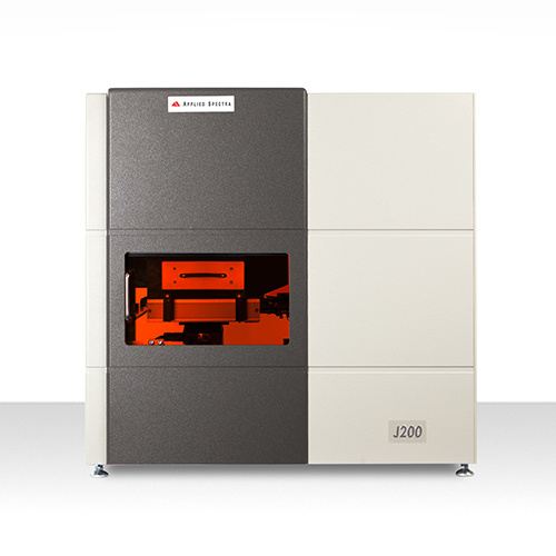
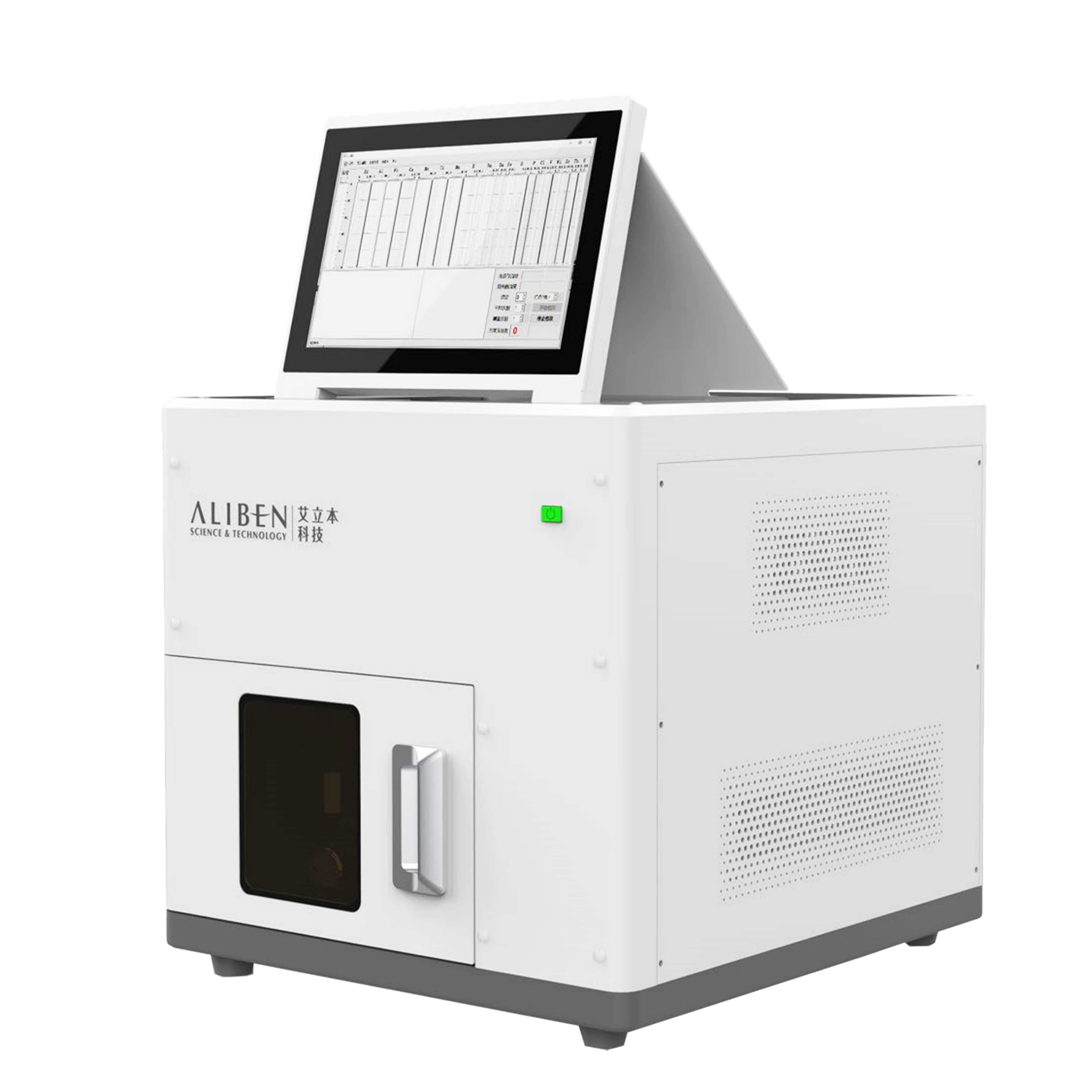
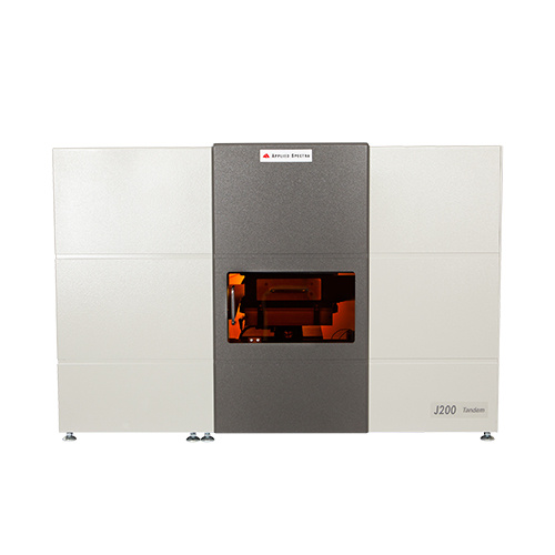
北京富尔邦科技发展有限责任公司为您提供《CuIn1-xGaxSe2太阳能电池薄膜中In、Ga、Mo检测方案(激光诱导击穿)》,该方案主要用于太阳能电池中In、Ga、Mo检测,参考标准--,《CuIn1-xGaxSe2太阳能电池薄膜中In、Ga、Mo检测方案(激光诱导击穿)》用到的仪器有美国ASI 激光诱导击穿光谱仪(LIBS)
推荐专场
相关方案
更多
该厂商其他方案
更多