
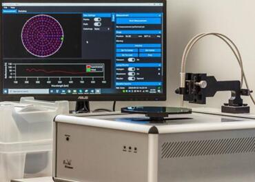


硅基传感器因其高性能、低成本和小尺寸而广泛应用于不同的微机电系统。悬挂在图案化硅膜或基于硅绝缘体的传感器上的活性硅层的厚度确定对于最终平台[1]的性能控制至关重要。在这里,我们已经在一个微机电系统压力传感器上测量了这样的薄膜厚度,使用的是一个孔径为250μm的FR-μ探针工具,该工具安装在一个徕卡分模光学显微镜上。使用10X物镜进行测量,该物镜与选定的孔径大小一起对应于25μm的光斑大小(测量区域)。
方案详情

Film Metrology & More...For further information, please contact us at info@thetametrisis.com or sales@thetametrisis.comThetaMetrisis C 2019, www.thetametrisis.com ThetaMetrisis APPLICATION NOTE #036 Suspended Active-Silicon membrane thickness measurements forMEMS applications, at a 25um spot size. Introduction: Silicon-based sensors have been broadly implemented in different MEMS applications for their high-performance, low cost and small size. Thickness determination of the active-Si layer either suspended on patterned Simembranes or on SOI based sensors is crucial for the control of the performance of the final platform [1]. Here wehave measured such film thicknesses on a MEMS pressure sensor, using the FR-uProbe tool with a 250um aperturesize, attached on a Leica DM LM optical microscope.Measurements performed using the 10X objective lens, whichalong with the selected aperture size, corresponds to a 25pm spot size (area of measurement). Means and Methods: Typical experimental reflectance spectra (black line) obtained, and fitted reflectance spectra(red line) as recorded by the FR-Monitor software, are illustrated in the figures below. Figure 1, shows measurementon the SOI area of the sensor, where simultaneous thickness measurement of Active-Silicon and the Buried Oxide wasperformed. The thickness value of the SiO2 thin film measured at 759.2nm, while the Si film on top at 5320.1 nm. Wavelenath Inm1 Figure 1. Experimental and fitted reflectance spectra of the SOl area on a MEMS pressure sensor and the thicknessvalues measured. Figure 2, shows measurement on the patterned suspended Silicon area of the sensor, where again the simultaneousthickness measurement of Active-Si and Buried Oxide was performed. The thickness value of the SiO2 thin filmmeasured to be the same at 759.2nm, while the Si film on top at 5329.1 um, 9nm higher than in the SOl area. Wavelenath Inm1 Figure 2. Experimental and fitted reflectance spectra of the suspended Silicon area on a MEMS pressure sensor and thethickness values measured. Concussions: ThetaMetrisis'FR-uProbe tool is a unique powerful tool for the local measurement of thickness(es) oflayers with spot size down to 2um. Thanks to its modular design can be attached on any trinocular optical microscopeenhancing this way the microscope capabilities without any effect on its performance. References: ( [1 . 1 ] J . J. Su, X . Zhang, G. Zhou, C. Xia, W. Zhou, and Q. Huang, “A review: crystalline silicon membranes over sealed cavities for pressure sensors by using silicon m igration technology,"j.Semicond., vol. 39, no. 7,pp. 1-7,2018. ) 悬浮式有源硅薄膜厚度测量,适用于微机电系统应用,光斑尺寸为25微米。简介:硅基传感器因其高性能、低成本和小尺寸而广泛应用于不同的微机电系统。悬挂在图案化硅膜或基于硅绝缘体的传感器上的活性硅层的厚度确定对于最终平台[1]的性能控制至关重要。在这里,我们已经在一个微机电系统压力传感器上测量了这样的薄膜厚度,使用的是一个孔径为250μm的FR-μ探针工具,该工具安装在一个徕卡分模光学显微镜上。使用10X物镜进行测量,该物镜与选定的孔径大小一起对应于25μm的光斑大小(测量区域)。测量方法:获得的典型实验反射光谱(黑线)和由FR-Monitor软件记录的拟合反射光谱(红线)显示了对传感器的SOI区域的测量,其中对活性硅和掩埋氧化物同时进行了厚度测量。二氧化硅薄膜的厚度值在759.2纳米测量,而硅薄膜在5320.1纳米测量。微机电系统压力传感器上硅绝缘体区域的实验和拟合反射光谱以及测量的厚度值。显示了对传感器的图案化悬浮硅区域的测量,其中再次执行了活性硅和掩埋氧化物的同时厚度测量。测得二氧化硅薄膜的厚度值在759.2纳米处相同,而硅薄膜在5329.1微米处的顶部,比硅绝缘体区域的厚度值高9纳米。微机电系统压力传感器上悬浮硅区域的实验和拟合反射光谱以及测量的厚度值。结论:参数测试系统的FR-uProbe工具是一个独特的强大工具,用于局部测量斑点尺寸低至2μm的层的厚度。由于其模块化设计,可安装在任何三眼光学显微镜上,从而增强显微镜的性能,而不会对其性能产生任何影响。FR的工具基于白光反射光谱(Reports) 。准确同步的厚度测量及薄膜的折射率-一个广泛的多样化的应用范围广泛的光电特性的工具和整体解决方案,如:半导体、有机电子、聚合物、涂料和涂料、光伏、生物传感、化学传感...
确定

还剩1页未读,是否继续阅读?

产品配置单


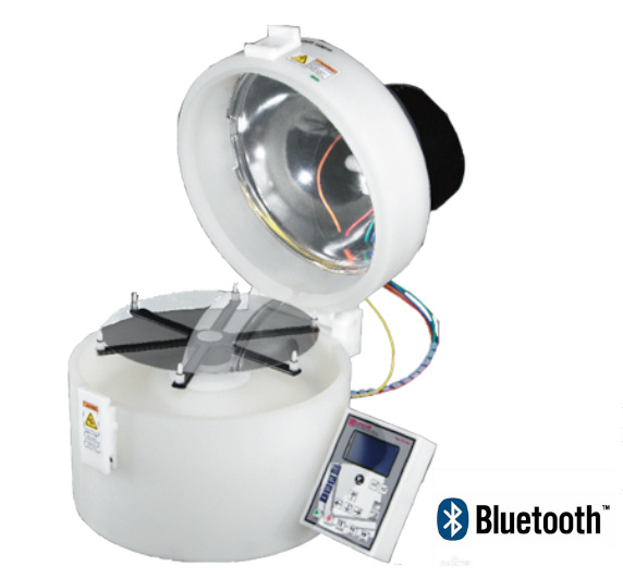
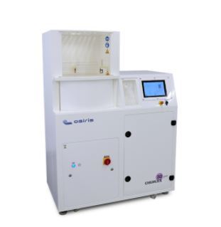
迈可诺技术有限公司为您提供《悬浮式活性硅中用于MEMS应用的悬浮式活性硅膜厚度测量检测方案(白光干涉测厚)》,该方案主要用于其他中用于MEMS应用的悬浮式活性硅膜厚度测量检测,参考标准--,《悬浮式活性硅中用于MEMS应用的悬浮式活性硅膜厚度测量检测方案(白光干涉测厚)》用到的仪器有扫描型光学膜厚仪 FR-Scanner、进口纳米狭缝涂布机、美国Laurell湿法刻蚀显影机EDC-650Mz-23NPP
推荐专场


相关方案
更多