


方案详情
文
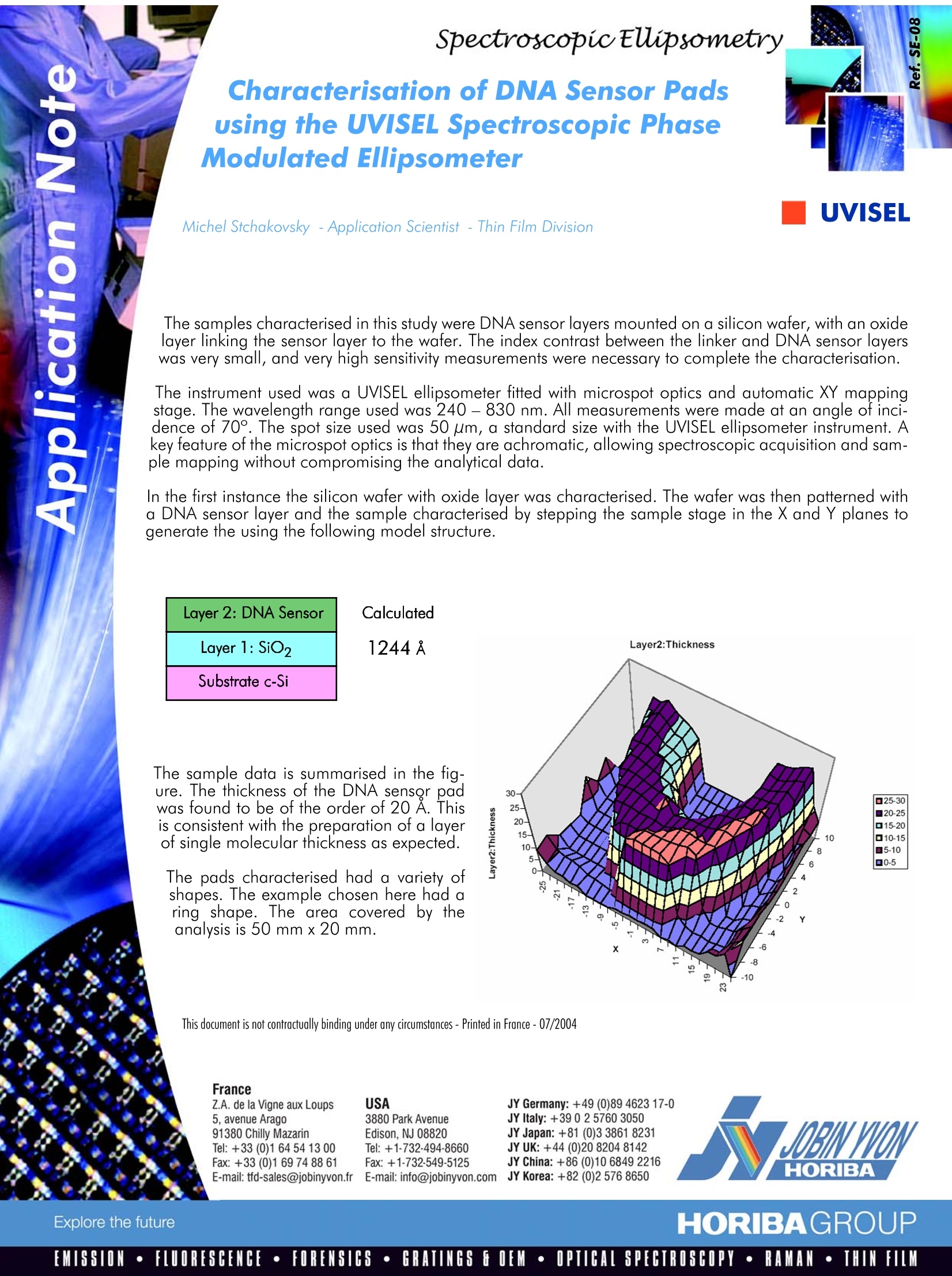
The sample data is summarised in the figure. The thickness of the DNA sensor pad was found to be of the order of 20 ?. This is consistent with the preparation of a layer of single molecular thickness as expected.
The pads characterised had a variety of shapes. The example chosen here had a ring shape. The area covered by the analysis is 50 mm x 20 mm.
方案详情

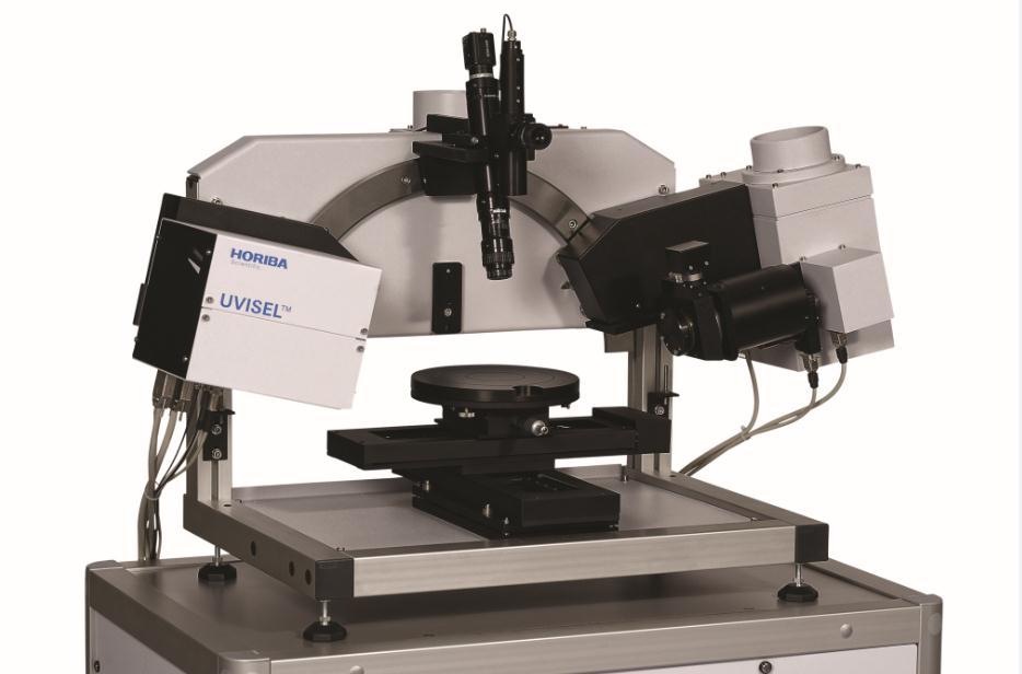
SpectroscopicEUipsometryExplore the futureEMISSION·FLUORESCENCE·FORENSICS·GRATINGS E OEM ·OPTICAL SPECTROSCOPY·RAMAN·THIN FILM Characterisation of DNA Sensor Padsusing the UVISEL Spectroscopic PhaseModulated Ellipsometer UVISEL Michel Stchakovsky - Application Scientist - Thin Film Division The samples characterised in this study were DNA sensor layers mounted on a silicon wafer, with an oxidelayer linking the sensor layer to the wafer. The index contrast between the linker and DNA sensor layerswas very small, and very high sensitivity measurements were necessary to complete the characterisation. The instrument used was a UVISEL ellipsometer fitted with microspot optics and automatic XY mappingstage. The wavelength range used was 240-830 nm. All measurements were made at an angle of inci-dence of 70°. The spot size used was 50 um, a standard size with the UVISEL ellipsometer instrument. Akey feature of the microspot optics is that they are achromatic, allowing spectroscopic acquisition and sam-ple mapping without compromising the analytical data. In the first instance the silicon wafer with oxide layer was characterised. The wafer was then patterned witha DNA sensor layer and the sample characterised by stepping the sample stage in the X and Y planes togenerate the using the following model structure. Layer 2: DNA SensorLayer1: SiO,Substrate c-Si Calculated 1244 A The sample data is summarised in the fig-ure. The thickness of the DNA sensor padwas found to be of the order of 20 A. Thisis consistent with the preparation ot a layerof single molecular thickness as expected. The pads characterised had a variety ofshapes. The example chosen here had aringshape. The area covered6by theanalysis is 50 mmx 20 mm. Z.A. de la Vigne aux Loups 5, avenue Arago 91380 Chilly Mazarin Tel:+33 (0)1 6454 1300 Fax: +33 (0)1 69 74 88 61 The sample data is summarised in the figure. The thickness of the DNA sensor pad was found to be of the order of 20 Å. This is consistent with the preparation of a layer of single molecular thickness as expected.The pads characterised had a variety of shapes. The example chosen here had a ring shape. The area covered by the analysis is 50 mm x 20 mm.
确定
还剩1页未读,是否继续阅读?

产品配置单

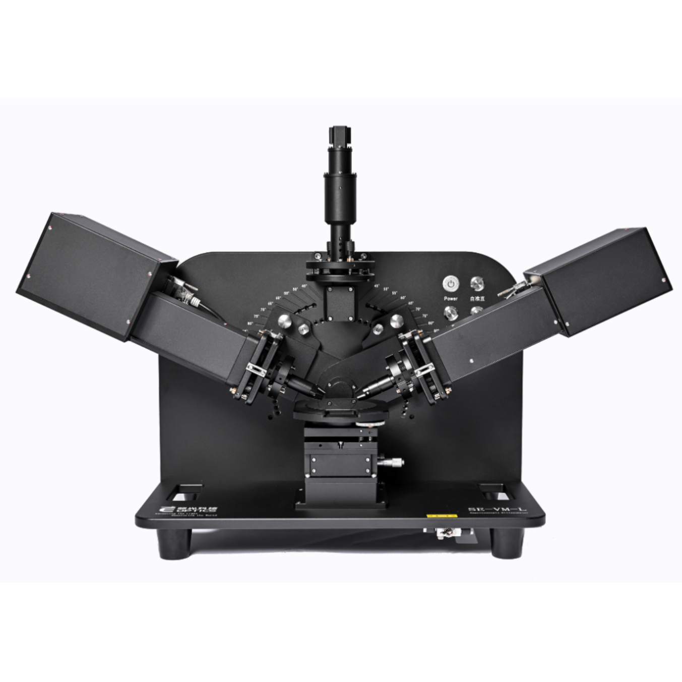
HORIBA(中国)为您提供《DNA传感器垫片中膜厚检测方案(椭偏仪)》,该方案主要用于其他中膜厚检测,参考标准--,《DNA传感器垫片中膜厚检测方案(椭偏仪)》用到的仪器有HORIBA UVISEL Plus研究级经典型椭偏仪
推荐专场
相关方案
更多
该厂商其他方案
更多