


方案详情
文
为了使光电(PV)发电提供世界能源需求的很大一部分,必须降低每瓦特产生的面板成本。低成本、高容量光伏发电的最佳前景是薄膜无机化合物,包括CdTe和Cu (In, Ga) Se2 (CIGS)。两种材料目前占太阳能电池板销量的20%,由于与硅相比有以下优势,这一比例可能会增加:1、这些材料的直接带隙意味着与100-400 μm的Si相比,所需的材料厚度大大减少,为2-5 μm。2、这种减少的厚度导致大大降低了对太阳能吸收器晶体质量的要求,它为更广泛的可能生产路线打开了大门;降低成本,提高产量。
方案详情

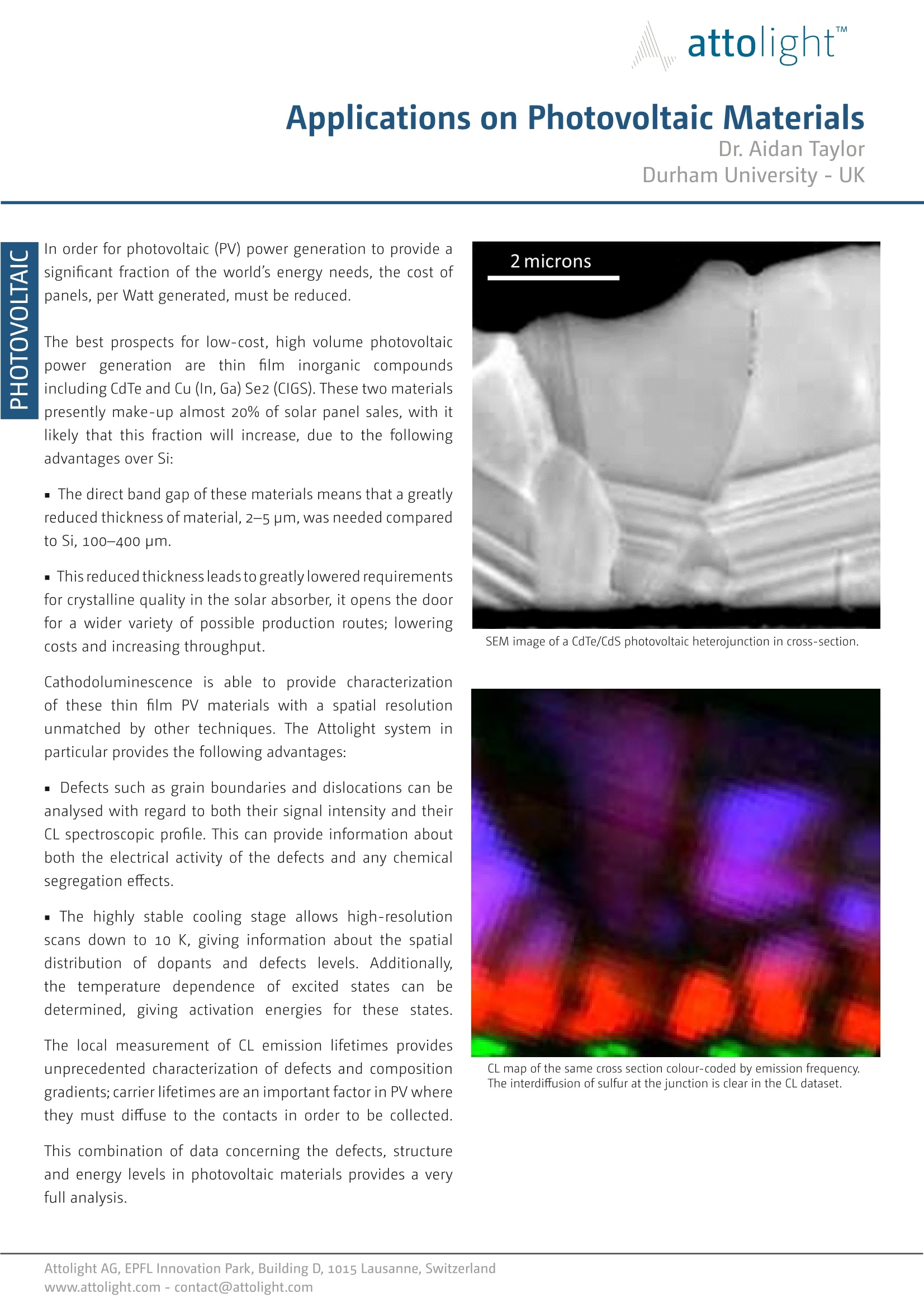
为了使光电(PV)发电提供世界能源需求的很大一部分,必须降低每瓦特产生的面板成本。低成本、高容量光伏发电的最佳前景是薄膜无机化合物,包括CdTe和Cu (In, Ga) Se2 (CIGS)。这两种材料目前占太阳能电池板销量的近20%,由于与硅相比有以下优势,这一比例可能会增加:1、这些材料的直接带隙意味着与100-400 μm的Si相比,所需的材料厚度大大减少,为2-5 μm。2、这种减少的厚度导致大大降低了对太阳能吸收器晶体质量的要求,它为更广泛的可能生产路线打开了大门;降低成本,提高产量。CdTe/CdS光伏异质结截面的SEM图像。阴极发光能够以其他技术无法比拟的空间分辨率提供这些薄膜PV材料的表征。Attolight系统尤其具有以下优点:1、晶界和位错等缺陷可以根据它们的信号强度和CL光谱剖面进行分析。这可以提供有关缺陷的电活动和任何化学分离效应的信息。2、高度稳定的冷却阶段允许低至10 K的高分辨率扫描,提供有关掺杂剂和缺陷水平的空间分布的信息。此外,可以确定激发态的温度依赖性,给出这些状态的活化能。同一截面的CL图,以发射频率的颜色编码。在CL数据集中,硫在连接处的相互扩散是清楚的。 局部测量CL发射寿命提供了前所未有的缺陷和成分梯度的表征,载流子寿命是PV中的一个重要因素,它们必须扩散到触点才能被收集。这一关于光伏材料缺陷、结构和能级的数据组合提供了一个非常全面的分析。Applications on Photovoltaic Materials Dr. Aidan Taylor Durham University- UK attolight In order for photovoltaic(PV) power generation to provide a signifciant fraction of the world’s energy needs, the cost of panels, per Watt generated, must be reduced. The best prospects for low-cost, high volume photovoltaic power generation are thin flim inorganic compounds including CdTe and Cu(In, Ga) Se2(CIGS). These two materials presently make-up almost 20% of solar panel sales, with it likely that this fraction will increase, due to the following advantages over Si: . The direct band gap of these materials means that a greatly reduced thickness of material, 2–5 pm, was needed compared to Si, 100–400 pm. · This reduced thickness leads to greatly lowered requirements for crystalline quality in the solar absorber, it opens the door for a wider variety of possible production routes; lowering costs and increasing throughput. Cathodoluminescenceisable toprovidecharacterization ofthesethinflimPVmaterialswithaspatialresolution unmatchedbyothertechniques.TheAttolightsystemin particular provides the following advantages: · Defects such as grain boundaries and dislocations can be analysed with regard to both their signal intensity and their CL spectroscopic proflie. This can provide information about both the electrical activity of the defects and any chemical segregation efefcts. Thehighlystablecoolingstageallowshigh-resolution scans down to 10 K, giving information about the spatial distribution of dopants and defects levels. Additionally, the temperature dependence of excited states can be determined, giving activation energies for these states. The local measurement of CL emission lifetimes provides unprecedented characterization of defects and composition gradients; carrier lifetimes are an important factor in PV where they must diffuse to the contacts in order to be collected. This combination of data concerning the defects, structure and energy levels in photovoltaic materials provides a very full analysis. SEM image of a CdTe/CdS photovoltaic heterojunction in cross-section. CL map of the same cross section colour-coded by emission frequency. The interdifufsion of sulfur at the junction is clear in the CL dataset.
确定
还剩1页未读,是否继续阅读?

产品配置单
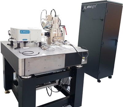
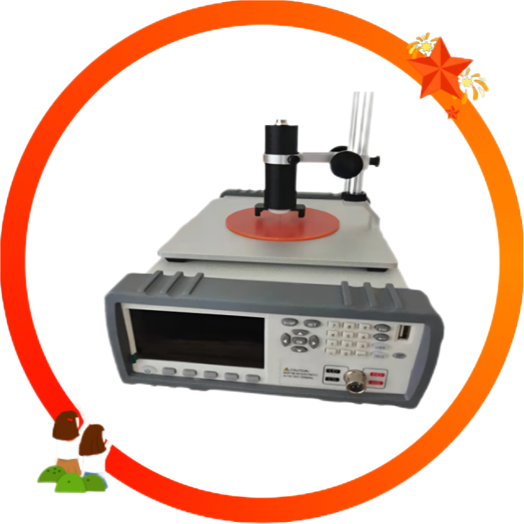
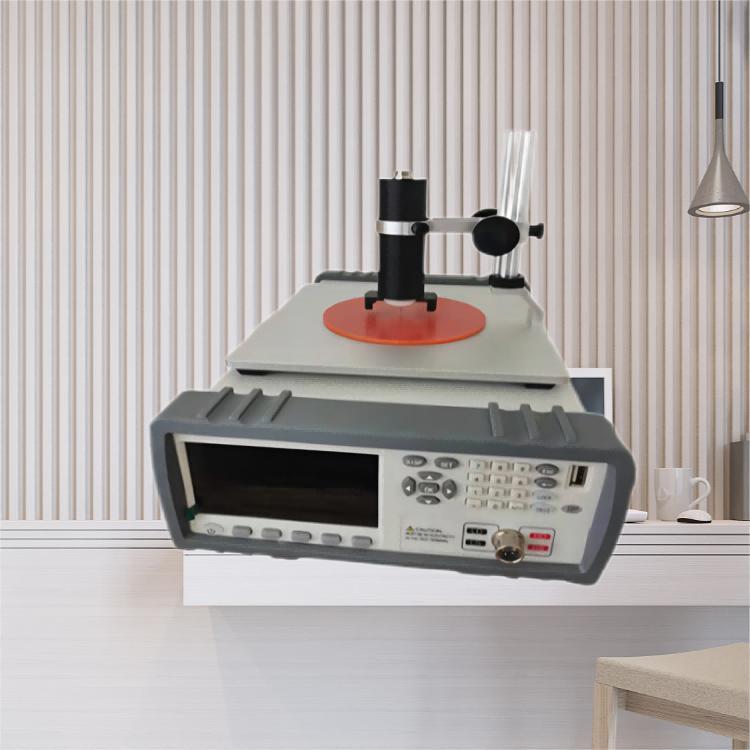
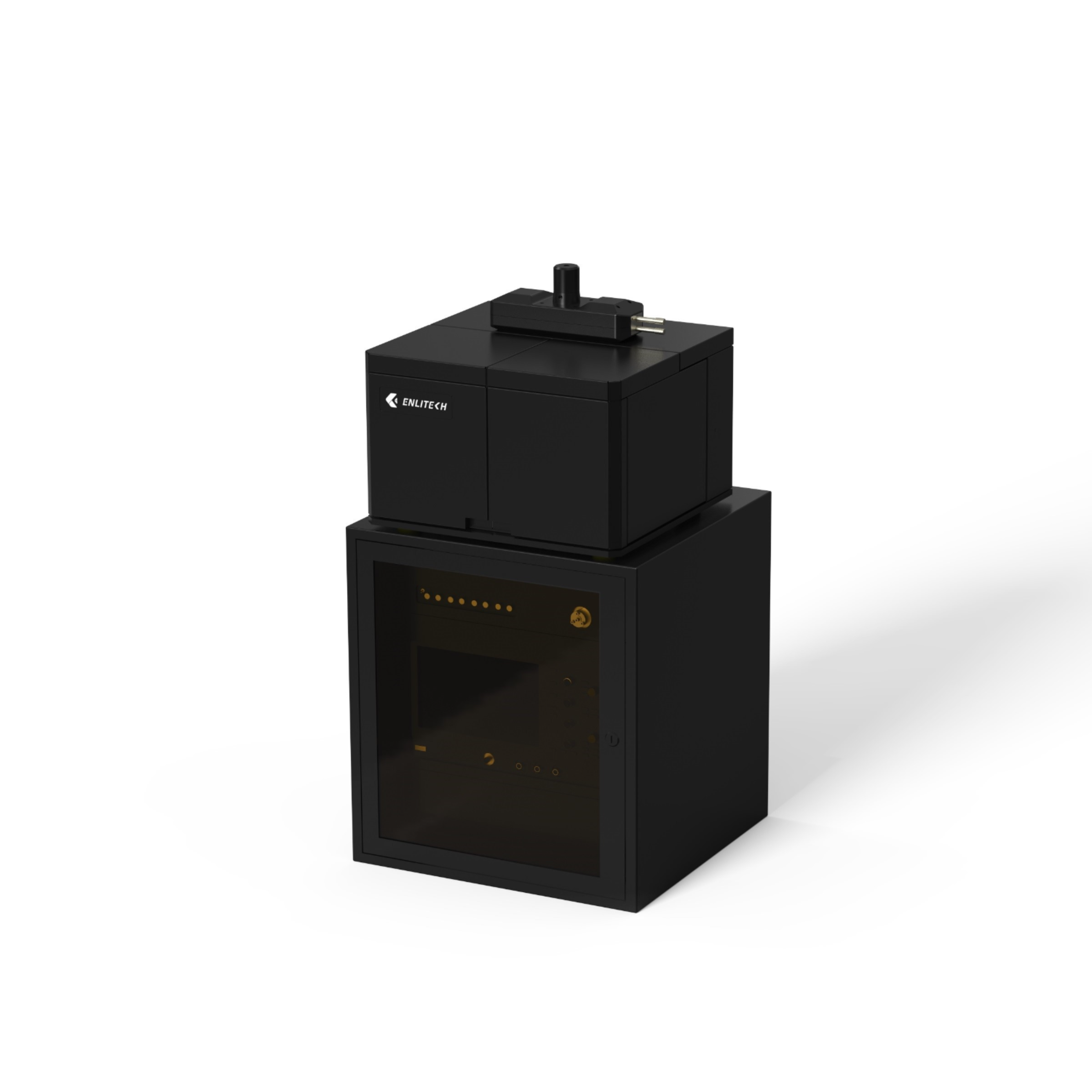
北京正通远恒科技有限公司为您提供《阴极发光设备(SEM-CL)在光伏材料方面的应用》,该方案主要用于其他中无检测,参考标准--,《阴极发光设备(SEM-CL)在光伏材料方面的应用》用到的仪器有快速定量阴极发光CL-SEM系统 Allalin
推荐专场
相关方案
更多