


方案详情
文
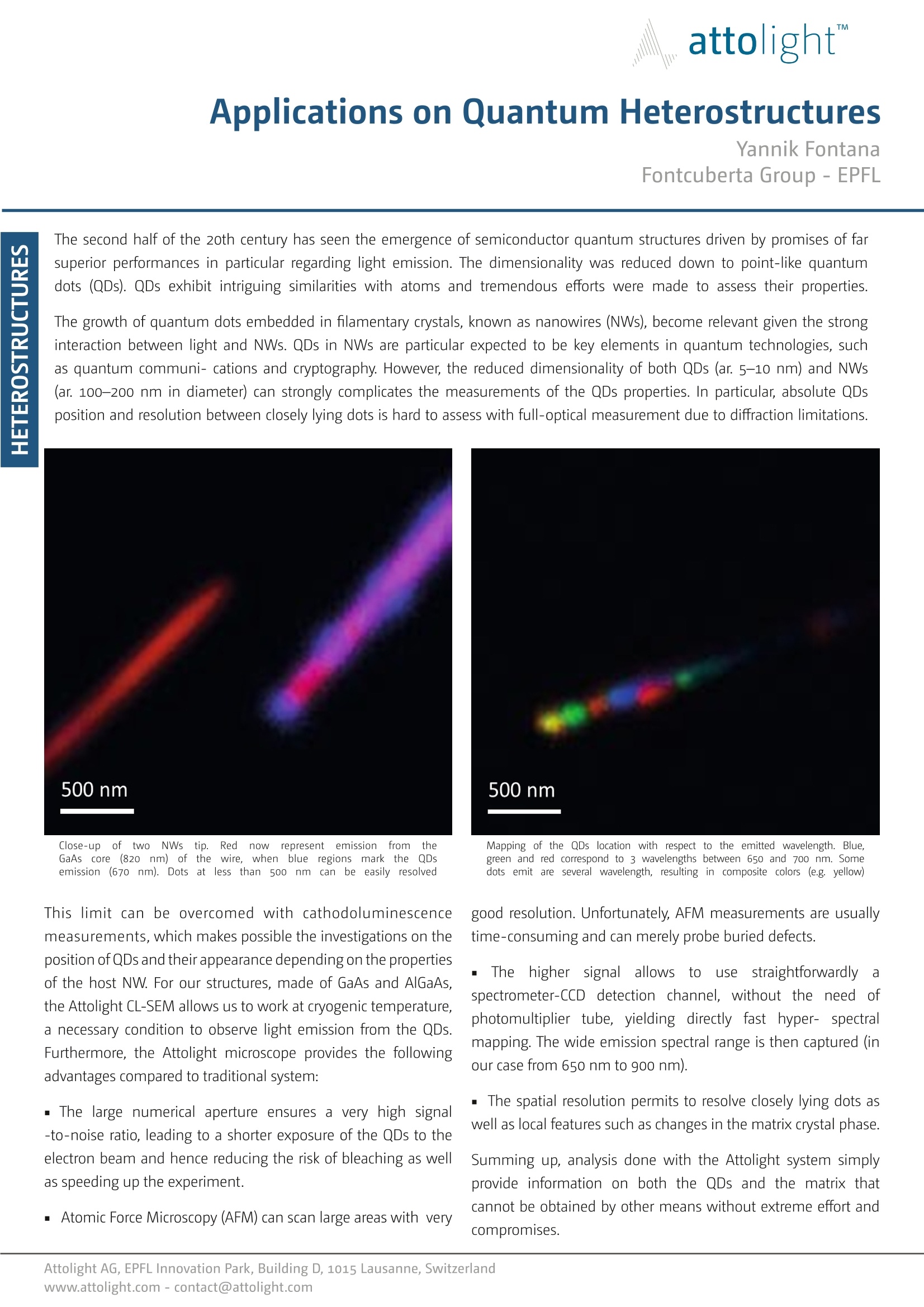
20世纪下半叶见证了半导体量子结构的出现,这是由于半导体量子结构在发光方面的卓越性能。将维数降为点状量子点(QDs),量子点与原子表现出有趣的相似之处,人们付出了巨大的努力来评估它们的性质。
考虑到光和纳米线之间的强相互作用,嵌入在被称为纳米线(NWs)的丝状晶体中的量子点的生长变得相关。NWs中的量子点尤其有望成为量子技术的关键要素,如量子通信和密码学。然而,量子点(约5-10 nm)和量子点的维数都降低了(直径约100 - 200nm)会使量子点性质的测量变得非常复杂。特别是,由于衍射的限制,很难用全光学测量来评估紧密放置点之间的绝对量子点位置和分辨率。
方案详情

20世纪下半叶见证了半导体量子结构的出现,这是由于半导体量子结构在发光方面的卓越性能。将维数降为点状量子点(QDs),量子点与原子表现出有趣的相似之处,人们付出了巨大的努力来评估它们的性质。 考虑到光和纳米线之间的强相互作用,嵌入在被称为纳米线(NWs)的丝状晶体中的量子点的生长变得相关。NWs中的量子点尤其有望成为量子技术的关键要素,如量子通信和密码学。然而,量子点(约5-10 nm)和量子点的维数都降低了(直径约100 - 200nm)会使量子点性质的测量变得非常复杂。特别是,由于衍射的限制,很难用全光学测量来评估紧密放置点之间的绝对量子点位置和分辨率。 这一限制可以通过阴极荧光测量来克服,这使得研究量子点的位置和它们的外观取决于宿主NW的性质成为可能。对于我们的结构,由砷化镓和砷化镓构成,Attolight CL-SEM允许我们在低温下工作,这是观测量子点发光的必要条件。此外,与传统系统相比,Attolight阴极荧光扫描电镜的优点如下:1、大的数值孔径确保了非常高的信噪比,从而缩短了量子点对电子束的暴露时间,从而降低了漂白的风险,并加快了实验速度。2、原子力显微镜(AFM)可以扫描大面积,分辨率很高。不幸的是,AFM测量通常是耗时的,只能探测隐藏的缺陷。3、更高的信号允许直接使用光谱- ccd检测通道,而不需要光电倍增管,直接产生快速的高光谱映射。然后捕获宽发射光谱范围(在我们的情况下从650 nm到900 nm)。4、空间分辨率允许解析靠近的点以及局部特征,如基质晶体相的变化。 综上所述,Attolight系统可以提供关于量子点和矩阵的信息,这些信息不能通过其他方式获得,除非付出极大的努力和妥协。两个NWs的特写提示。红色表示从金属线的gaas核心(820 nm)发射,而蓝色区域表示量子点发射(670 nm)量子点位置相对于发射波长的映射。蓝色、绿色和红色对应650到700纳米之间的3个波长。Applications on Quantum Heterostructures Yannik Fontana Fontcuberta Group - EPFL The second half of the 20th century has seen the emergence of semiconductor quantum structures driven by promises of far superior performances in particular regarding light emission. The dimensionality was reduced down to point-like quantum dots (QDs). QDs exhibit intriguing similarities with atoms and tremendous efofrts were made to assess their properties. The growth of quantum dots embedded in fliamentary crystals, known as nanowires (NWs), become relevant given the strong interaction between light and NWs. QDs in NWs are particular expected to be key elements in quantum technologies, such as quantum communi- cations and cryptography. However, the reduced dimensionality of both QDs (ar. 5–10 nm) and NWs (ar. 100–200 nm in diameter) can strongly complicates the measurements of the QDs properties. In particular, absolute QDs position and resolution between closely lying dots is hard to assess with full-optical measurement due to difrfaction limitations. Close-up of two NWs tip. Red now represent emission from the GaAs core (820 nm) of the wire, when blue regions mark the QDs emission (670 nm). Dots at less than 500 nm can be easily resolved Thislimit canbeovercomedwithcathodoluminescence measurements, which makes possible the investigations on the position of QDs and their appearance depending on the properties of the host NW. For our structures, made of GaAs and AlGaAs, the Attolight CL-SEM allows us to work at cryogenic temperature, a necessary condition to observe light emission from the QDs. Furthermore, the Attolight microscope provides the following advantages compared to traditional system: Thelargenumerical apertureensuresaveryhighsignal -to-noise ratio, leading to a shorter exposure of the QDs to the electron beam and hence reducing the risk of bleaching as well as speeding up the experiment. · Atomic Force Microscopy (AFM) can scan large areas with very Mapping of the QDs location with respect to the emitted wavelength. Blue, greenandredcorrespondto3wavelengthsbetween650and700nm.Some dots emit are several wavelength, resulting in composite colors (e.g. yellow) good resolution. Unfortunately, AFM measurements are usually time-consuming and can merely probe buried defects. ■The higher signal allows to use straightforwardly a spectrometer-CCD detection channel, without the need of photomultiplier tube, yielding directly fast hyper- spectral mapping. The wide emission spectral range is then captured (in our case from 650 nm to 900 nm). · The spatial resolution permits to resolve closely lying dots as well as local features such as changes in the matrix crystal phase. Summing up, analysis done with the Attolight system simply provideinformationon boththeQDsandthematrixthat cannot be obtained by other means without extreme effort and compromises.
确定
还剩1页未读,是否继续阅读?

产品配置单
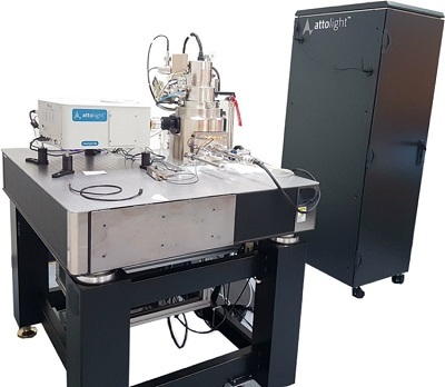
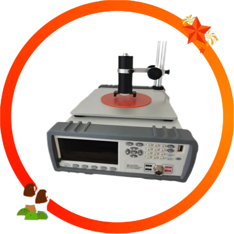
北京正通远恒科技有限公司为您提供《阴极发光设备(SEM-CL)在量子异质结构方面的应用》,该方案主要用于其他中量子异质结构检测,参考标准--,《阴极发光设备(SEM-CL)在量子异质结构方面的应用》用到的仪器有快速定量阴极发光CL-SEM系统 Allalin
推荐专场
相关方案
更多
该厂商其他方案
更多