


方案详情
文
测量厚度的光学方法适用于各种材料的研究和开发,如新型电介质和半导体涂层。这些方法的主要优点是提供无损和非接触的测量,以及从亚nm到!m的广泛测量范围。JASCO可以根据薄膜厚度、多层数和基材提供最合适的测量和分析方法
方案详情

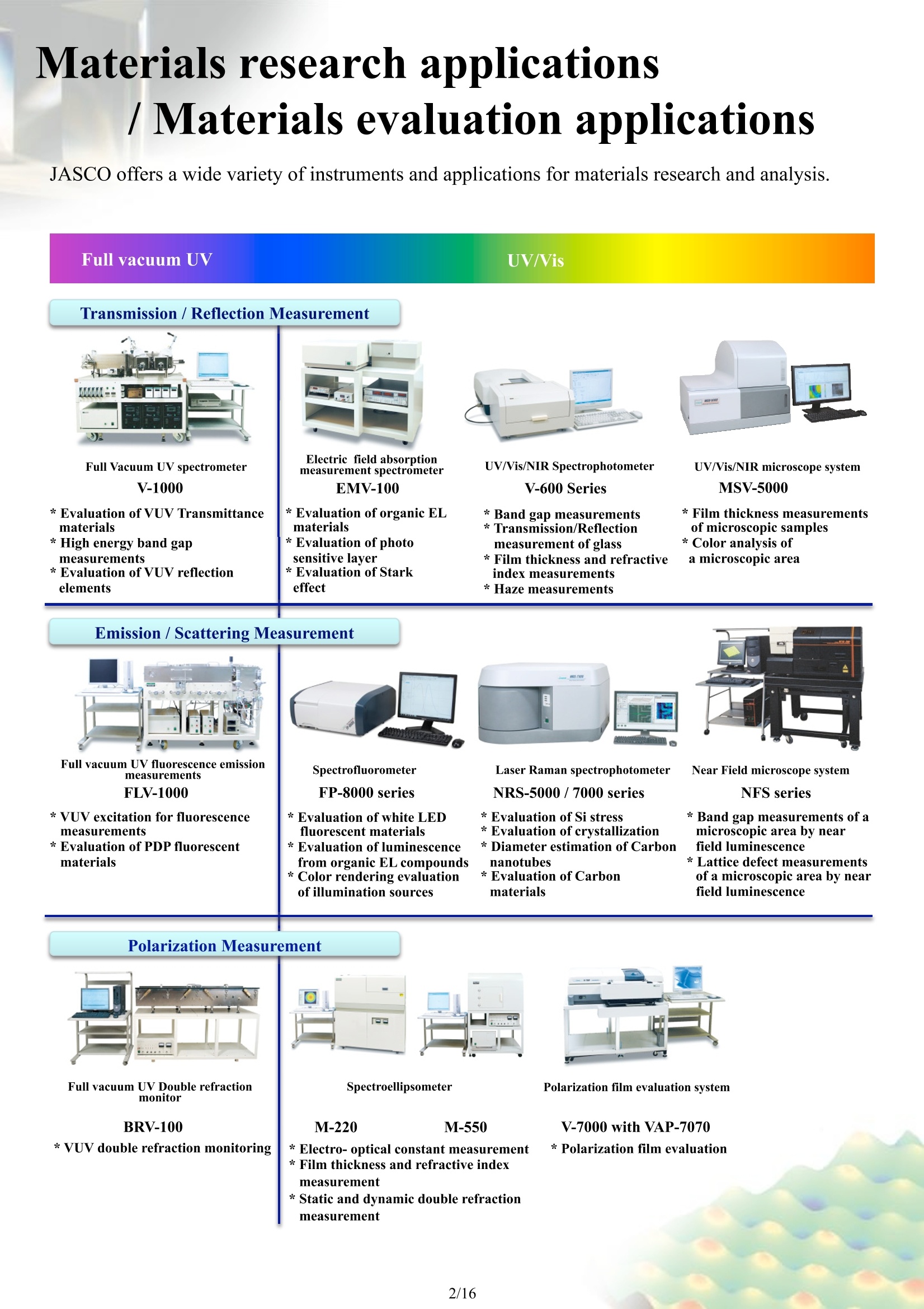
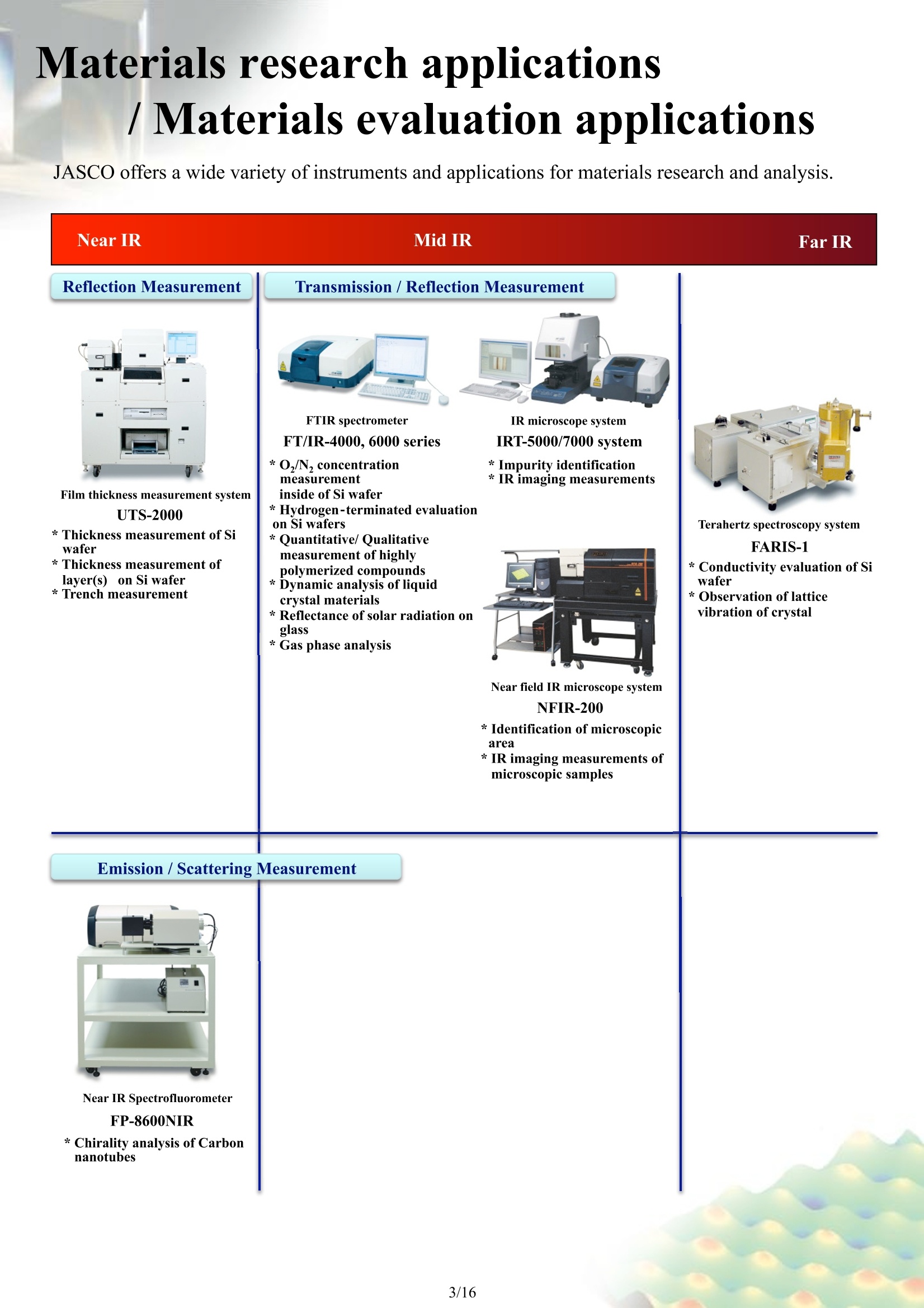
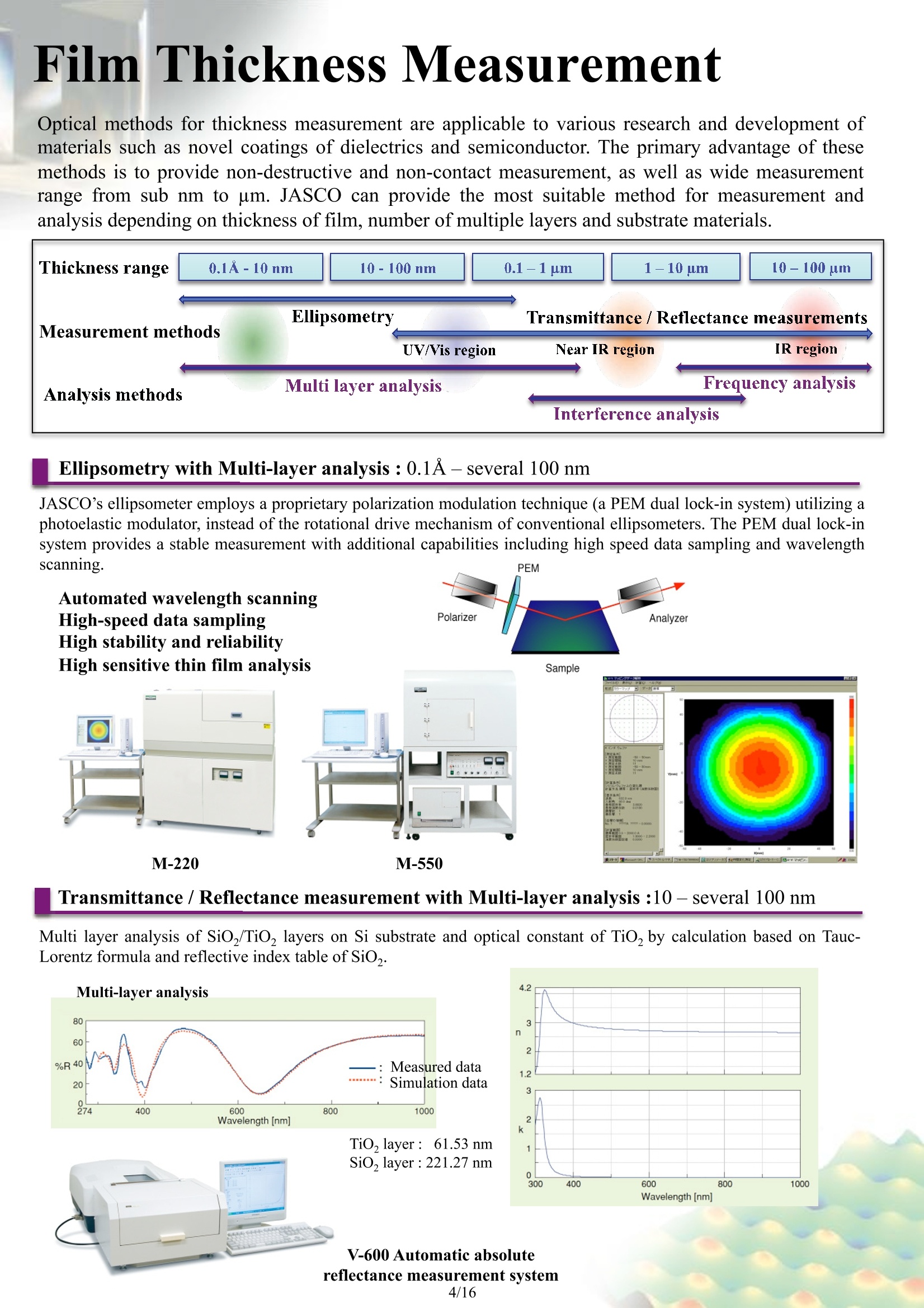
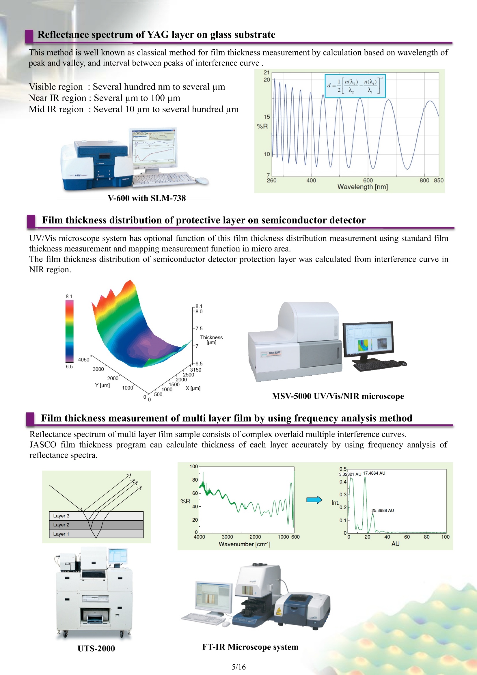
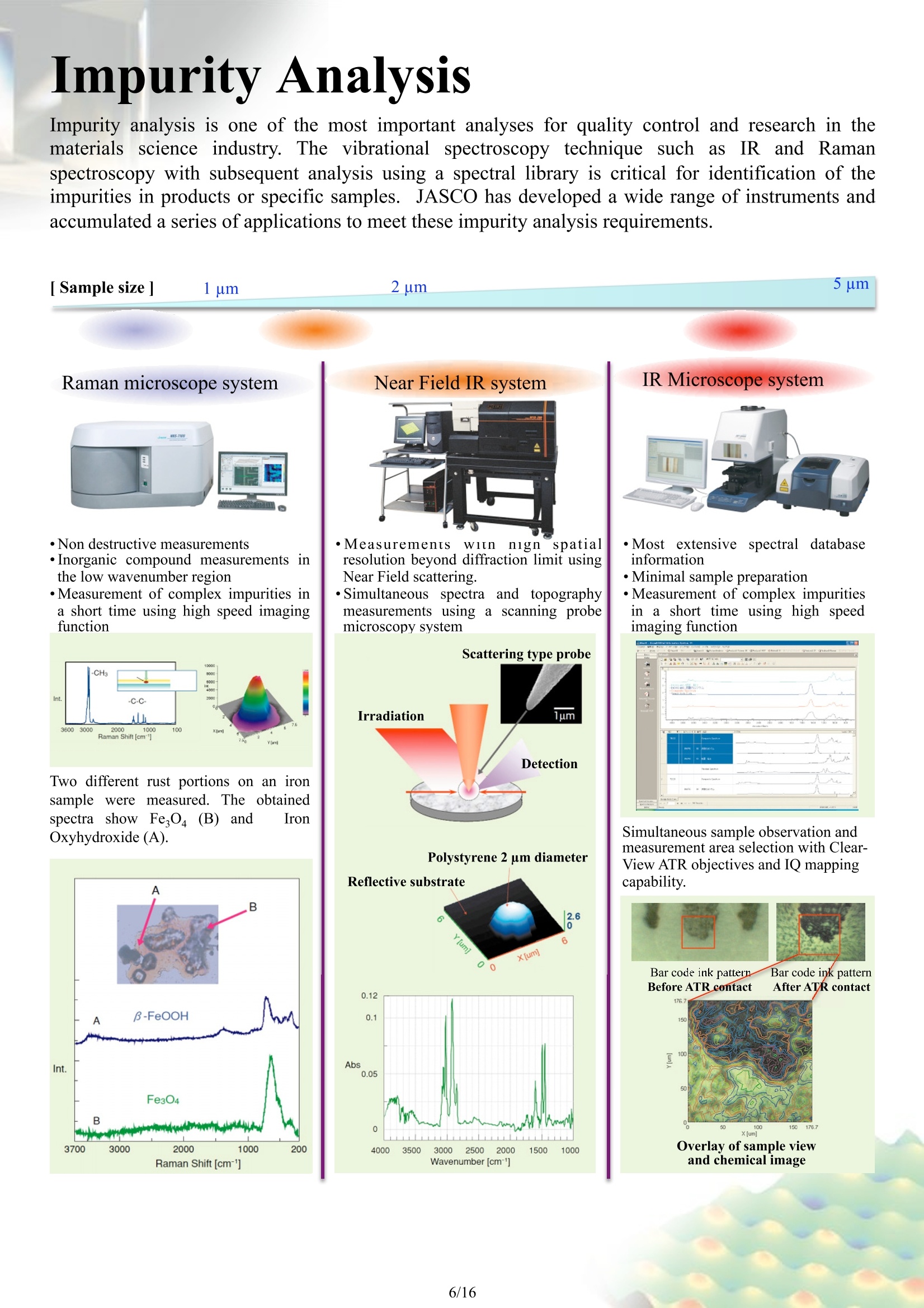
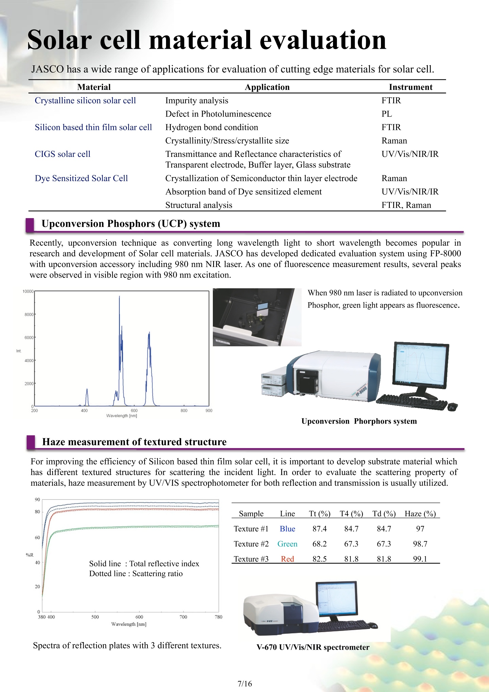
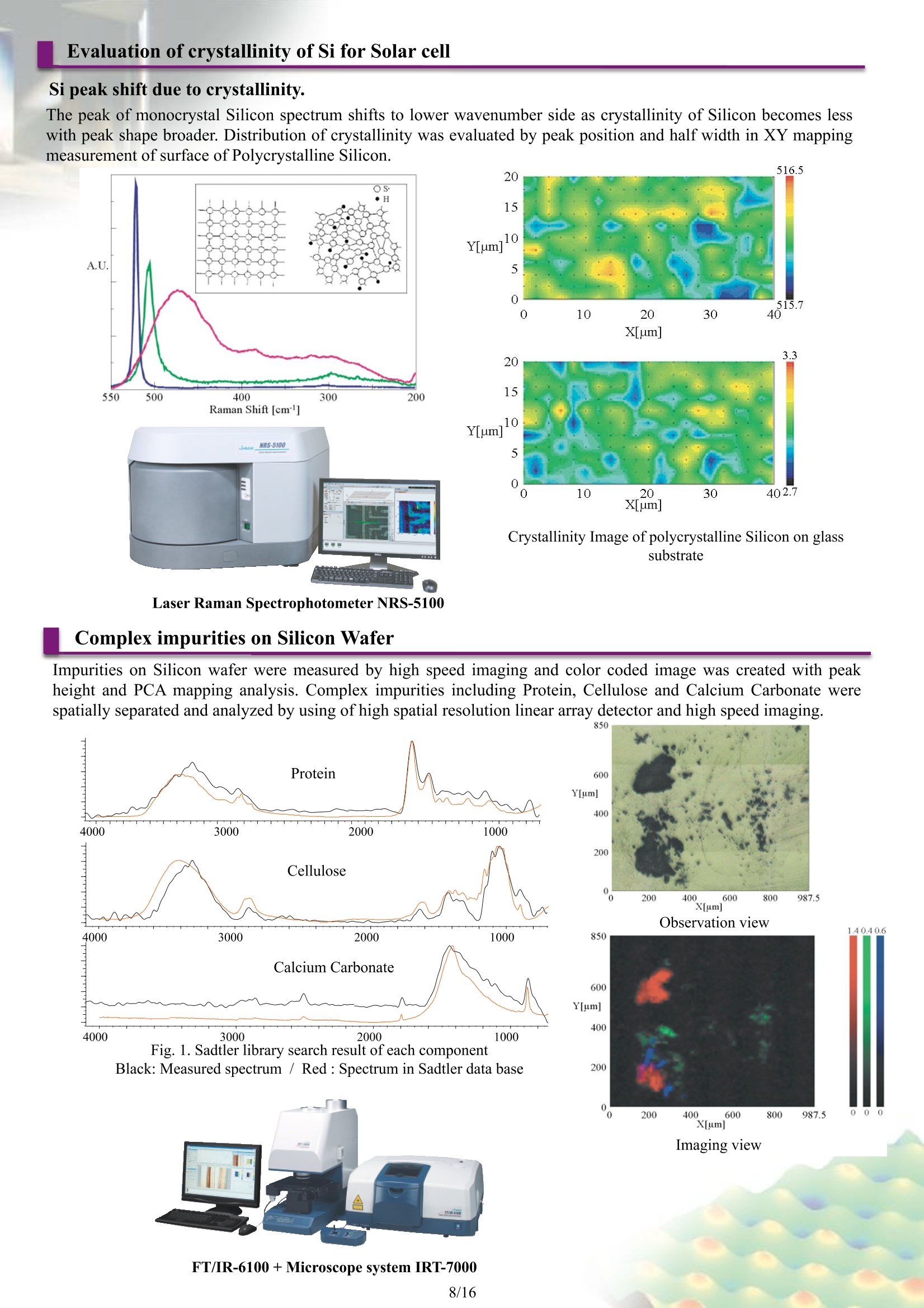
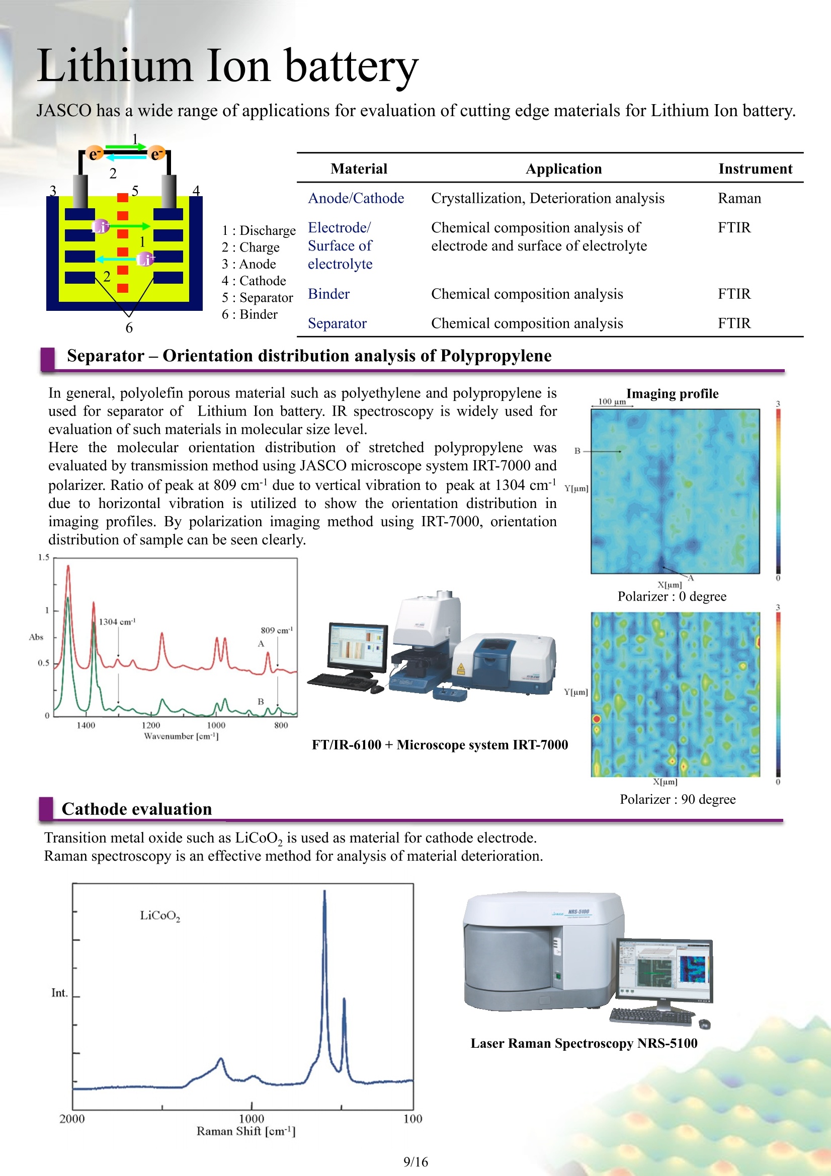
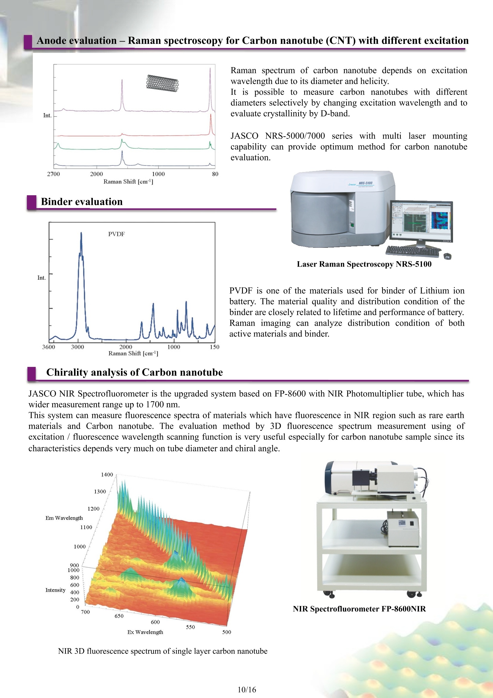
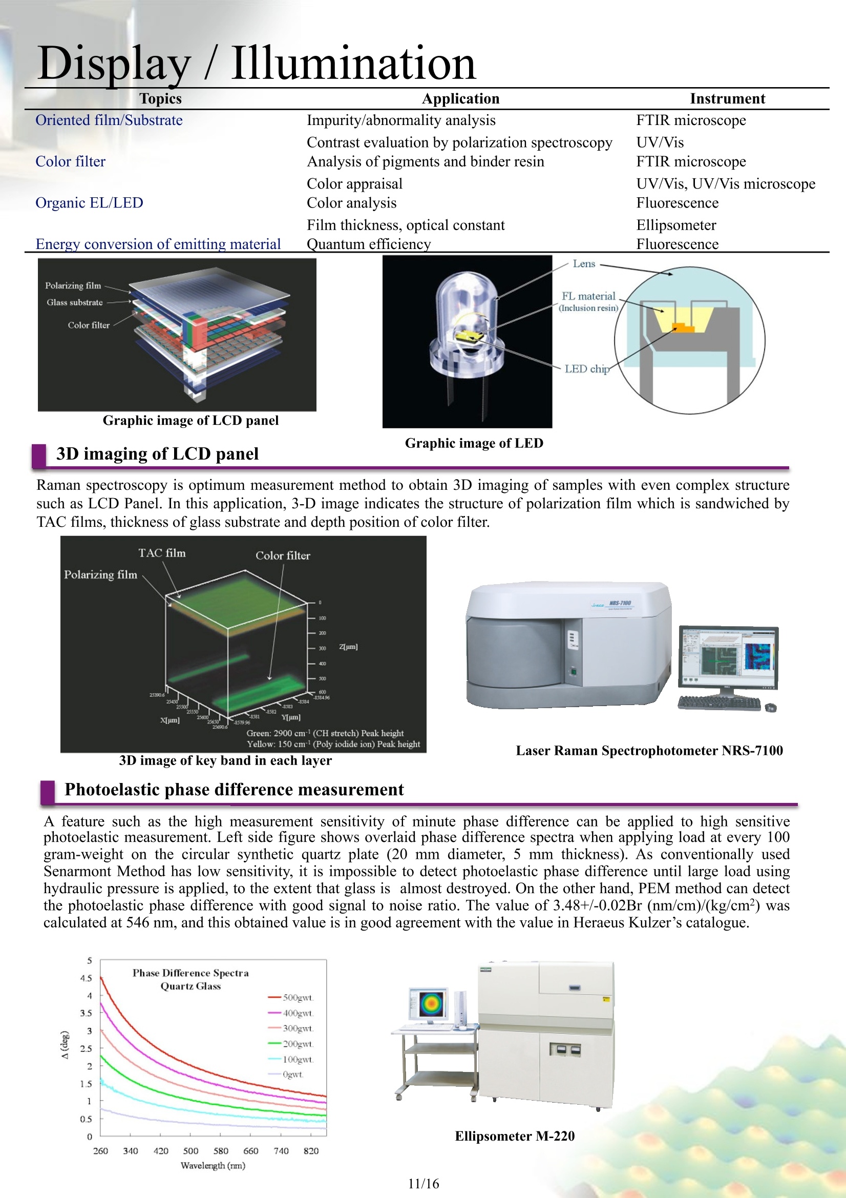
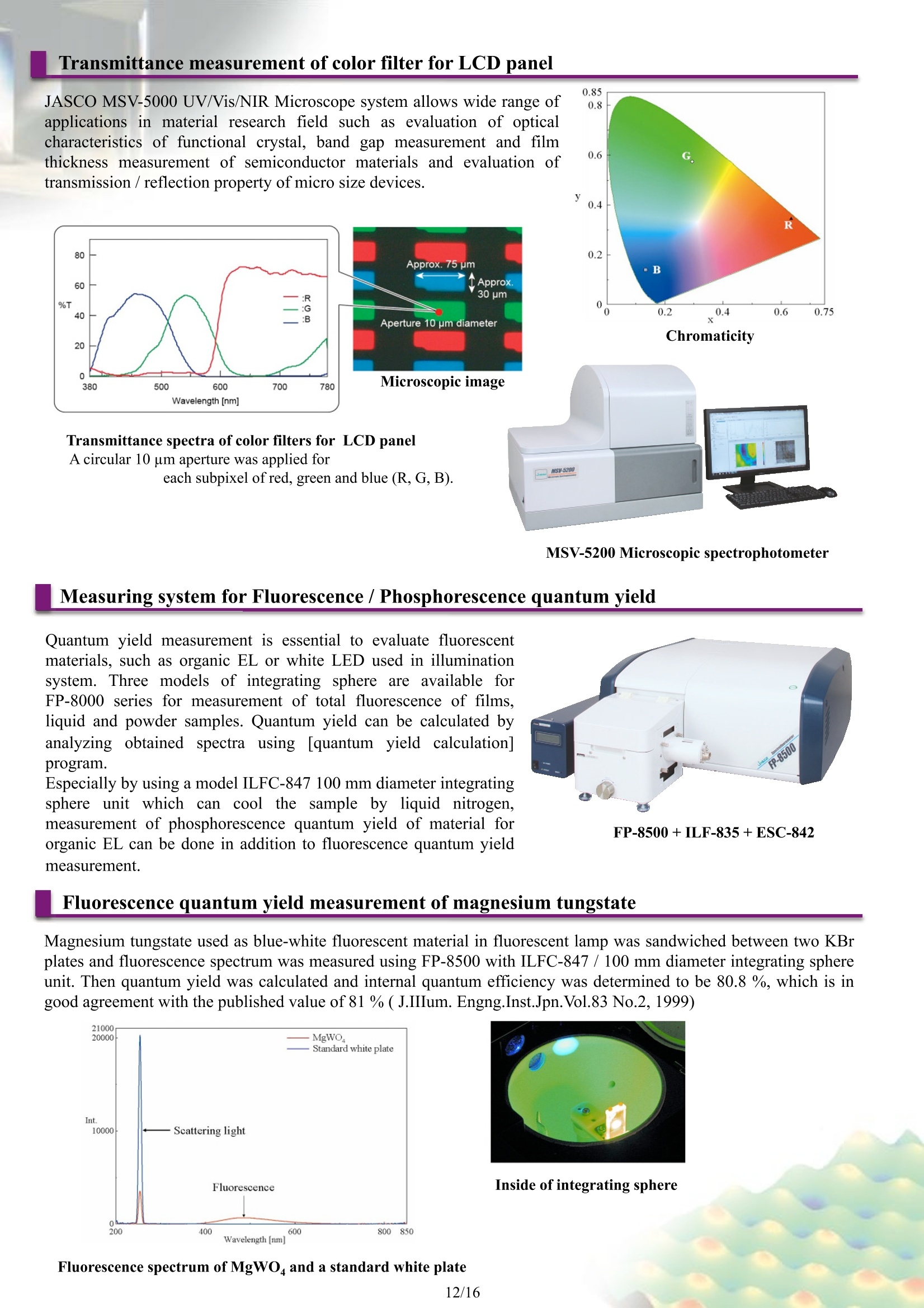
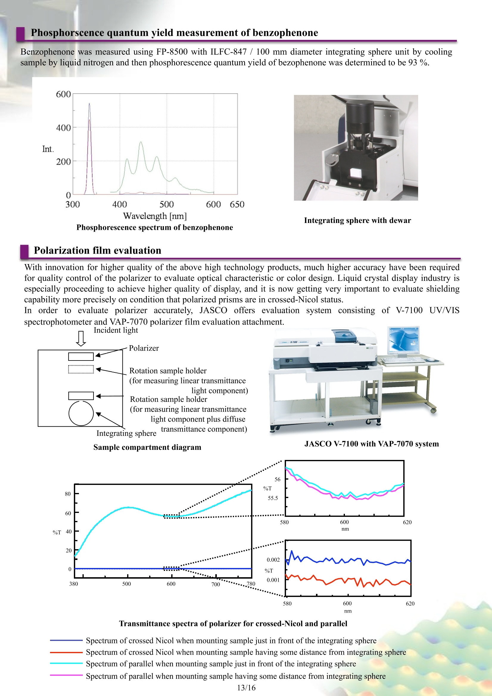
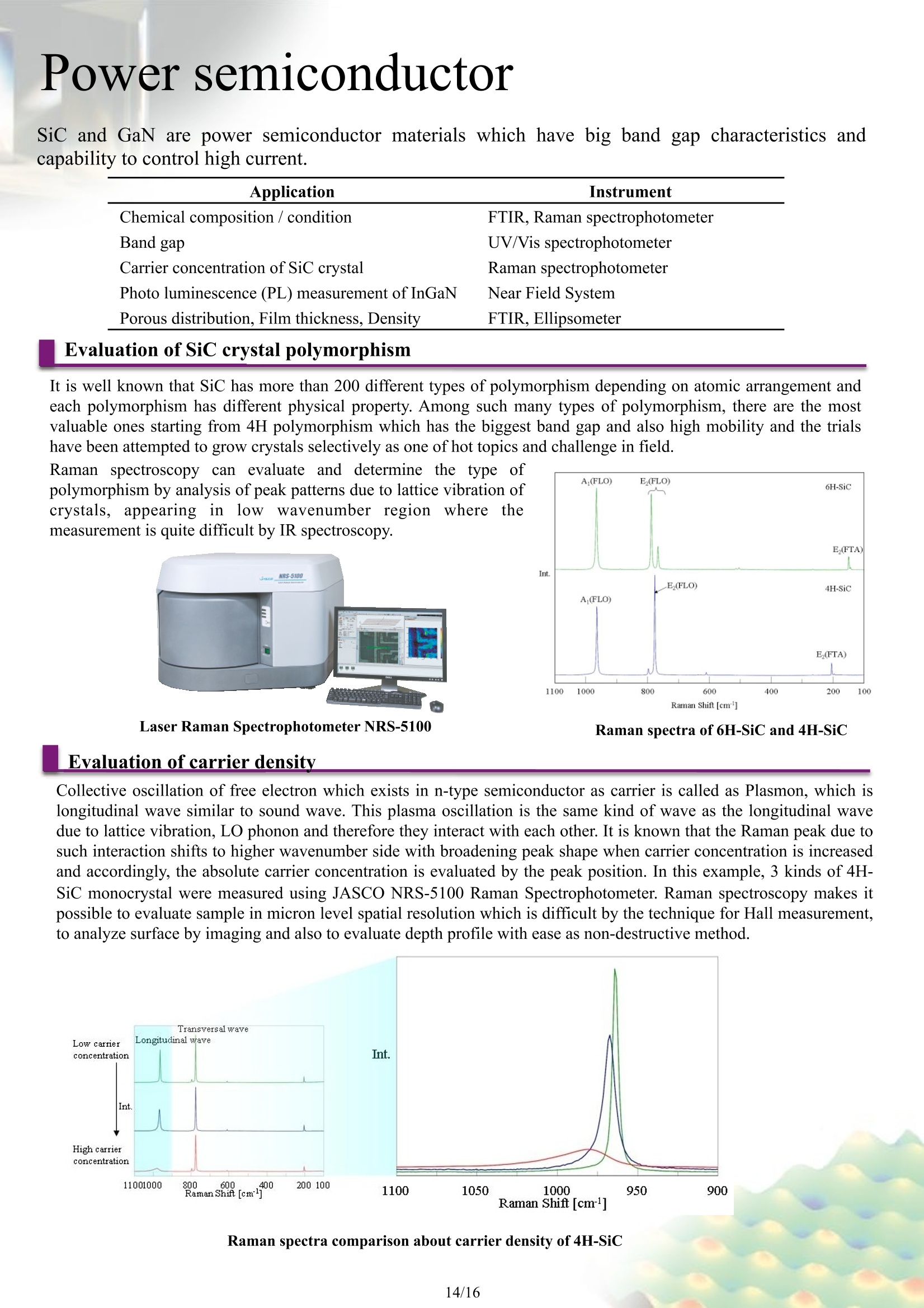
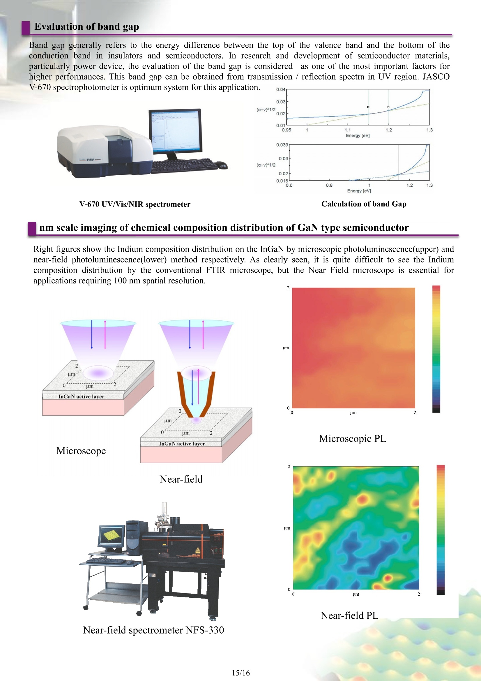
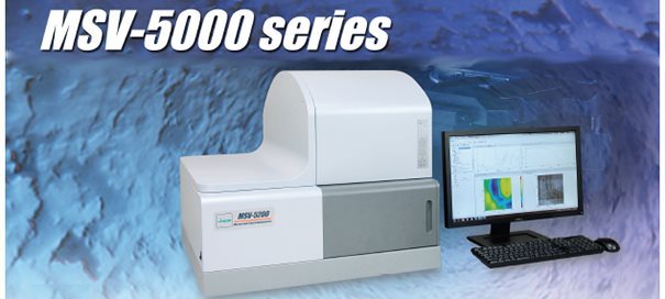
测量厚度的光学方法适用于各种材料的研究和开发,如新型电介质和半导体涂层。这些方法的主要优点是提供无损和非接触的测量,以及从亚nm到!m的广泛测量范围。JASCO可以根据薄膜厚度、多层数和基材提供最合适的测量和分析方法。Evaluation of crystallinity of Si for Solar cell Anode evaluation - Raman spectroscopy for Carbon nanotube (CNT) with different excitation Applications and Solutions For Research and Development in Material and Semiconductor field Materials research applications /Materials evaluation applications JASCO offers a wide variety of instruments and applications for materials research and analysis. Full vacuum U V * Evaluation of VUV Transmittance materials *High energy band gap measurements * Evaluation of VUV reflection elements Emission / Scattering Measurement Ful l vacuum UV fluorescence emission measurements FLV-1000 Spectrofluorometer FP-8000 series Laser Raman spectrophotometer Near Field microscope system NRS-5000/7000 series NFS series * VUV excitation for fluorescence measurements *Evaluation of white LED * Evaluation of Si stress * Band gap measurements of a fluorescent materials * Evaluation of crystallization microscopic area by near * Evaluation of PDP fluorescent materials * Evaluation of luminescence * Diameter estimation of Carbon field luminescence from organic EL compounds nanotubes * Lattice defect measurements * Color rendering evaluation * Evaluation of Carbon of a microscopic area by near of illumination sources materials field luminescence P o lar i zat ion Me a su re ment Ful l vacuum UV Double refraction monitor Spectroellipsometer Polarization film evaluation system BRV-100 M-220 M-550 V-7000 with VAP-7070 * VUV double refraction monitoring * Electro- optical constant measurement * Film thickness and refractive index measurement * Polarization film evaluation * Static and dynamic double refraction measurement Materials research applications / Materials evaluation applications JASCO offers a wide variety of instruments and applications for materials research and analysis. Film Thickness Measurement Optical methods for thickness measurement are applicable to various research and development of materials such as novel coatings of dielectrics and semiconductor. The primary advantage of these methods is to provide non-destructive and non-contact measurement, as wel l as wide measurement range from sub nm to um. JASCO can provide the most suitable method for measurement and analysis depending on thickness of film, number of multiple layers and substrate materials. Ellipsometry with Multi-layer analysis : 0.1A-several 100 nm JASCO's ellipsometer employs a proprietary polarization modulation technique (a PEM dual lock-in system) utilizing a photoelastic modulator, instead of the rotational drive mechanism of conventional ellipsometers. The PEM dual lock-in system provides a stable measurement with additional capabilities i ncluding high speed data sampling and wavelength scanning. PEM Transmittance/Reflectance measurement with Multi-layer analysis :10 - several 100 nm Multi layer analysis of SiO,/TiO, layers on Si substrate and optical constant of TiO, by calculation based on Tauc-Lorentz formula and reflective index table of SiO.. Reflectance spectrum of YAG layer on glass substrate This method is well known as classical method for f ilm thickness measurement by calculation based on wavelength of peak and val l ey, and interval between peaks of interference curve . Visible region : Several hundred nm to several um Near IR region : Several um to 100 um Mid IR region : Several 10 um to several hundred um Film thickness distribution of protective layer on semiconductor detector UV/Vis microscope system has optional function of this film t hickness distribut i on measurement using standard f ilm thickness measurement and mapping measurement function in micro area. The f ilm thickness distribution of semiconductor detector protection layer was calculated from interference curve in NIR region. MSV-5000 UV/Vis/NIR microscope Film thickness measurement of multi layer film by using frequency analysis method Reflectance spectrum of multi layer film sample consists of complex overlaid multiple interference curves.JASCO film thickness program can calculate thickness of each layer accurately by using frequency analysis of reflectance spectra. UTS-2000 FT-IR Microscope system Impurity Analysis Impurity analysis is one of the most important analyses for quality control and research in the materials science industry. The vibrational spectroscopy technique such as IR and Raman spectroscopy with subsequent analysis using a spectral library is critical for identification of the impurities in products or specific samples.JASCO has developed a wide range of instruments and accumulated a series of applications to meet these impurity analysis requirements. [ Sample size ] 1pm 2um 5um Raman microscope system ·Non destructive measurements ·Inorganic compound measurements in the low wavenumber region ·Measurement of complex impurities in a short time using high speed imaging f unction Two different rust portions on an iron samplee were measured. The obtained spectra show Fe;04 (B) and Iron Oxyhydroxide (A). A B A B -FeOOH I n t . F e 3O4 B 3700 3000 2000 1000 200 Near Field IR system 0.05 0 4000 3500 300025002000 1500 1000 W aven u m be r [c m 】 ·Most extensivee:spectral 1database information · Minima l sample preparation ·Measurement of complex impurities in12a short time using high speed imaging function :2....0....... 一 Simul t aneous sample observation and measurement area selection with Clear-View ATR objectives and IQ mapping capabi l ity. Solar cell material evaluation JASCO has a wide range of applications for evaluation of cutt i ng edge materials for solar cell. Material Application Instrument Crystalline silicon solar cell Impurity analysis FTIR Defect in Photoluminescence PL Silicon based thin film solar cell Hydrogen bond condition FTIR Crystallinity/Stress/crystallite size Raman CIGS solar cell Transmittance and Reflectance characteristics of Transparent electrode, Buffer layer, Glass substrate Crystallization of Semiconductor thin layer electrode UV/Vis/NIR/IR Dye Sensitized Solar Cell Raman Absorption band of Dye sensitized element UV/Vis/NIR/IR Structural analysis FTIR,Raman Upconversion Phosphors (UCP) system Recently, upconversion technique as converting long wavelength light to short wavelength becomes popular in research and development of Solar cell materials. JASCO has developed dedicated evaluation system using FP-8000with upconversion accessory including 980 nm NIR laser. As one of fluorescence measurement results, several peaks were observed i n visible region with 980 nm exc i tation . Upconversion Phorphors system Haze measurement of textured structure For i mproving t he effic i ency of Silicon based thin film solar cell, it is important to develop substrate material which has different textured structures for scattering the incident light. In order to evaluate the scattering property of materials, haze measurement by UV/VIS spectrophotometer for both reflection and transmission is usually utilized. Sample Line Tt(%) T4(%) Td(%) Haze (%) Texture #1 Blue 87.4 84.7 84.7 97 Texture #2 Green 68.2 67.3 67.3 98.7 Texture #3 Red 82.5 81.8 81.8 99.1 Spectra of reflection plates with 3 different textures. V-670 UV/Vis/NIR spectrometer Si peak shift due to crystallinity. The peak of monocrystal Silicon spectrum shifts to lower wavenumber side as crystallinity of Silicon becomes less with peak shape broader. Distribution of crystallinity was evaluated by peak position and half width in XY mapping measurement of surface of Polycrystall i ne Silicon. Raman Shi ft [c m ]N RS-5100 Laser Raman Spectrophotometer NRS-5100 Complex impurities on Silicon Wafer X[um] Crystal l inity Image of polycrystall i ne Silicon on glass substrate Fig. 1. Sadtler library search result of each component Black: Measured spectrum / Red : Spectrum in Sadtler data base FT/IR-6100 +Microscope system IRT-7000 850 Observation view Imaging view Lithium Ion battery JASCO has a wide range of applications for evaluation of cutting edge materials for Lithium Ion battery. Material Application Instrument Anode/Cathode eElectrode/Surface ofelectrolyte Binder Separator Crystallization, Deterioration analysis Raman Chemical composition analysis of FTIR electrode and surface of electrolyte Chemical composition analysis FTIR Chemical composition analysis FTIR Separator- Orientation distribution analysis of Polypropylene In general, polyolefin porous material such as polyethylene and polypropylene is used for separator of Lithium Ion battery. IR spectroscopy is widely used for evaluation of such materials in molecular size level. Here the molecular orientation distribution of stretched polypropylene was evaluated by transmission method using J ASCO microscope system IRT-7000 and polarizer. Ratio of peak at 809 cm due to vertical vibration to peak at 1304 cm--1due to horizontal vibration is utilized to show the orientation distribution in imaging profiles. By polarization imaging method using IRT-7000, orientation distribution of sample can be seen clearly. X [um] Polarizer : 0 degree FT/IR-6100+Microscope system IRT-7000 0 Polarizer : 90 degree Cathode evaluation Transition metal oxide such as LiCoO, i s used as material for cathode electrode.Raman spectroscopy is an effective method for analysis of material deterioration. Laser Raman Spectroscopy NRS-5100 Raman Shi f t [cm] It i i s s possible to measure carbon nanotubes with different diameters selectively by changing excitation wavelength and to evaluate crystall i nity by D-band. JASCO NRS-5000/7000 series V with multi laser mounting capability can provide optimum method for carbon nanotube evaluation. Laser Raman Spectroscopy NRS-5100 PVDF is one of the materials used for binder of Lithium ion battery. The material quality and distribution condition of the binder are closely related to lifetime and performance of battery.Raman imaging can analyze distribution condition of both active materials and binder. Chirality analysis of Carbon nanotube JASCO NIR Spectrofluorometer is the upgraded system based on FP-8600 with NIR Photomultiplier tube, which has wider measurement range up to 1700 nm. This system can measure fluorescence spectra of materials which have fluorescence in NIR region such as rare earth materials and Carbon nanotube. The evaluation method by 3D fluorescence spectrum measurement using of excitation / fluorescence wavelength scanning function is very useful especially for carbon nanotube sample since i ts characteristics depends very much on tube diameter and chiral angle. NIR Spectrofluorometer FP-8600NIR Topics Application Instrument Oriented film/Substrate Impurity/abnormality analysis FTIR microscope Contrast evaluation by polarization spectroscopy UV/Vis Color filter Analysis of pigments and binder resin Color appraisal FTIR microscope Organic EL/LED UV/Vis, UV/Vis microscope Color analysis Fluorescence Film thickness, optical constant Ellipsometer Energy conversion of emitting material Quantum efficiency Fluorescence L en s Graphic image of LED 3D imaging of LCD panel Raman spectroscopy is opt i mum measurement method to obtain 3D imaging of samples with even complex structure such as LCD Panel. In this application, 3-D i mage indicates the structure of polarization film which is sandwiched by TAC films, thickness of glass substrate and depth position of color filter. Photoelastic phase difference measurement A feature such as the high measurement sensitivity of minute phase difference can be applied to high sensitive photoelastic measurement. Lef t side figure shows overlaid phase difference spectra when applying load at every 100gram-weight on the circular synthetic quartz plate (20 mm diameter, 5 mm thickness). As conventionally used Senarmont Method has low sensitivity, it i s i mpossible to detect photoelastic phase difference until large load using hydraulic pressure i s applied, to the extent that glass is almost destroyed. On the other hand, PEM method can detect the photoelastic phase dif f erence with good signal to noise ratio. The value of 3.48+/-0.02Br (nm/cm)/(kg/cm²) was calculated at 546 nm, and t his obtained value is i n good agreement with the value i n Heraeus Kulzer's catalogue. Ellipsometer M-220 JASCO MSV-5000 UV/Vis/NIR Microscope system allows wide range of applications in material research field such as evaluation of optical characteristics of functional crystal, band gap measurement and f i lm thickness measurement of semiconductor materials and evaluation of transmission / reflection property of micro size devices. Chromaticity Transmittance spectra of color filters for LCD panel A circular 10 um aperture was applied for each subpixel of red, green and blue (R, G, B). MSV-5200 Microscopic spectrophotometer Measuring system for Fluorescence /Phosphorescence quantum yield Quantum yield measurement is essential to evaluate fluorescent materials, such as organic EL or white LED used in illumination system. Three models of integrating sphere are available for FP-8000 series for measurement of total fluorescence of films,liquid and powder samples. Quantum yield can be calculated by analyzing obtained spectra using [quantum yield calculation]program. Especially by using a model ILFC-847 100 mm diameter integrating sphere unit which can cool the sample e by liquid nitrogen,measurement of phosphorescence quantum yield of material for organic EL can be done in addition to f luorescence quantum yield measurement. Fluorescence quantum yield measurement of magnesium tungstate Magnesium tungstate used as blue-white fluorescent material in fluorescent lamp was sandwiched between two KBr plates and f luorescence spectrum was measured using FP-8500 with ILFC-847 / 100 mm diameter integrating sphere unit. Then quantum yield was calculated and i nternal quantum efficiency was determined to be 80.8 %, which is i n good agreement with the published value of 81 % (J.II I um. Engng.Inst.Jpn.Vol.83 No.2, 1999) Inside of integrating sphere Fluorescence spectrum of MgWO and a standard white plate Benzophenone was measured using FP-8500 with ILFC-847 / 100 mm diameter integrating sphere unit by cooling sample by liquid nitrogen and then phosphorescence quantum yield of bezophenone was determined to be 93 %. Integrating sphere with dewar Phosphorescence spectrum of benzophenone Polarization film evaluation With i nnovation for higher quality of the above high technology products, much higher accuracy have been required for quality control of the polarizer to evaluate optical characteristic or color design. Liquid crystal display industry is especially proceeding to achieve higher quality of display, and i t is now gett i ng very important to evaluate shielding capabi l ity more precisely on condition that polarized prisms are in crossed-Nicol status. In order to evaluate polarizer accurately, JASCO offers evaluationn system consisting of V-7100 UV/VIS spectrophotometer and VAP-7070 polarizer film evaluation attachment. Incident l ight Sample compartment diagram JASCO V-7100 with VAP-7070 system nm Transmittance spectra of polarizer for crossed-Nicol and parallel Spec t rum of crossed Nicol when mounting sample just in f ront of the integrat i ng sphere Spec t rum of crossed Nicol when mounting sample having some distance from i ntegrating sphere Spectrum of parallel when mounting sample just i n front of the i ntegrating sphere Spectrum of paralle l when mounting sample having some distance from integrating sphere Power semiconductor SiC and GaN are power semiconductor materials which have big band gap characteristics and capability to control high current. Application Instrument Chemical composition / condition FTIR, Raman spectrophotometer Band gap UV/Vis spectrophotometer Carrier concentration of SiC crystal Raman spectrophotometer Photo luminescence (PL) measurement of InGaN Near Field System Porous distribution, Film thickness, Density FTIR, Ellipsometer Evaluation of SiC crystal polymorphism It is well known that SiC has more than 200 different types of polymorphism depending on atomic arrangement and each polymorphism has different physical property. Among such many types of polymorphism, there are the most valuable ones starting from 4H polymorphism which has the biggest band gap and also high mobil i ty and the t rials have been attempted to grow crystals selectively as one of hot topics and challenge in f ield. Raman spectroscopy can evaluate and determine the type of polymorphism by analysis of peak patterns due to lattice vibration of crystals, appearing in low wavenumber region where the measurement is quite difficult by IR spectroscopy. A(FLO) E (FL O) Raman spectra of 6H-SiC and 4H-SiC Evaluation of carrier density Collective oscillation of free electron which exists in n-type semiconductor as carrier is called as Plasmon, which is longitudinal wave similar to sound wave. This plasma osc i llation is the same kind of wave as the longitudinal wave due to lattice vibration, LO phonon and therefore they i nteract with each other. I t is known that the Raman peak due to such interaction shifts to higher wavenumber side with broadening peak shape when carrier concentration is i ncreased and accordingly, the absolute carrier concentration i s evaluated by the peak position. In this example, 3 kinds of 4H-SiC monocrystal were measured using JASCO NRS-5100 Raman Spectrophotometer. Raman spectroscopy makes it possible to evaluate sample in micron level spatial resolution which is difficult by the technique for Hall measurement,to analyze surface by imaging and also to evaluate depth profile with ease as non-destructive method. Raman spectra comparison about carrier density of 4H-SiC Evaluation of band gap Band gap generally refers to the energy difference between the top of the valence band and the bottom of the conduction band in insulators and semiconductors. In research and development of semiconductor materials,particularly power device, the evaluation of the band gap is consideredas one of the most important factors for higher performances. This band gap can be obtained from transmission / reflection spectra in UV region. JASCO V-670 spectrophotometer i s optimum system for this application. 0.04 nm scale imaging of chemical composition distribution of GaN type semiconductor Right f igures show the Indium composition distribution on the InGaN by microscopic photoluminescence(upper) and near-field photoluminescence(lower) method respectively. As clearly seen, it is quite difficult to see the Indium composition distribution by the conventional FTIR microscope, but the Near Field microscope is essential for applications requiring 100 nm spatial resolution. Microscopic PL Near-field Near-field PL Near-field spectrometer NFS-330 Other applications Quantitative analysis of light element impurity in silicon In order to evaluate the quality of wafer, i t i s important to analyze the concentration of oxygen and carbon in silicon material. For establishing the reliable analysis method, JASCO supplies FT/IR-6000 system with dedicated software to measure oxygen and carbon with ease and analyze quantitatively. The system can also evaluate molecular bonding state of Si-H, Si-H, in amorphous silicon and Si-H and N-H in silicon nitride fi l m. Fourier Transform Infrared Spectrometer FT/IR-6000 Gas analysis system in semiconductor field Quantitative analysis of O2 in Silicon In order to measure accurately low level gas concentration, i t is essential to select long path gas cel l and to remove influence from CO, and H,O in air. JASCO supplies FT/IR-6300FV, full vacuum type with 12M gas cell as the most suitable system for high sensitive gas analysis. FT/IR-6300FV+12M gas cell Optical characteristics evaluation of semiconductor laser JASCO Near-field system can evaluate optical characteristics of semiconductor laser in nano scale. Generally, this evaluation method consists of radiation pattern analysis, electric luminescence distribution and wavelength of luminescence. in position B
确定
还剩14页未读,是否继续阅读?

产品配置单

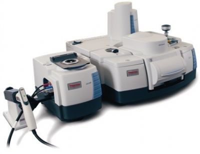
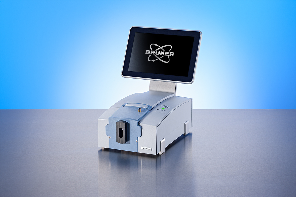
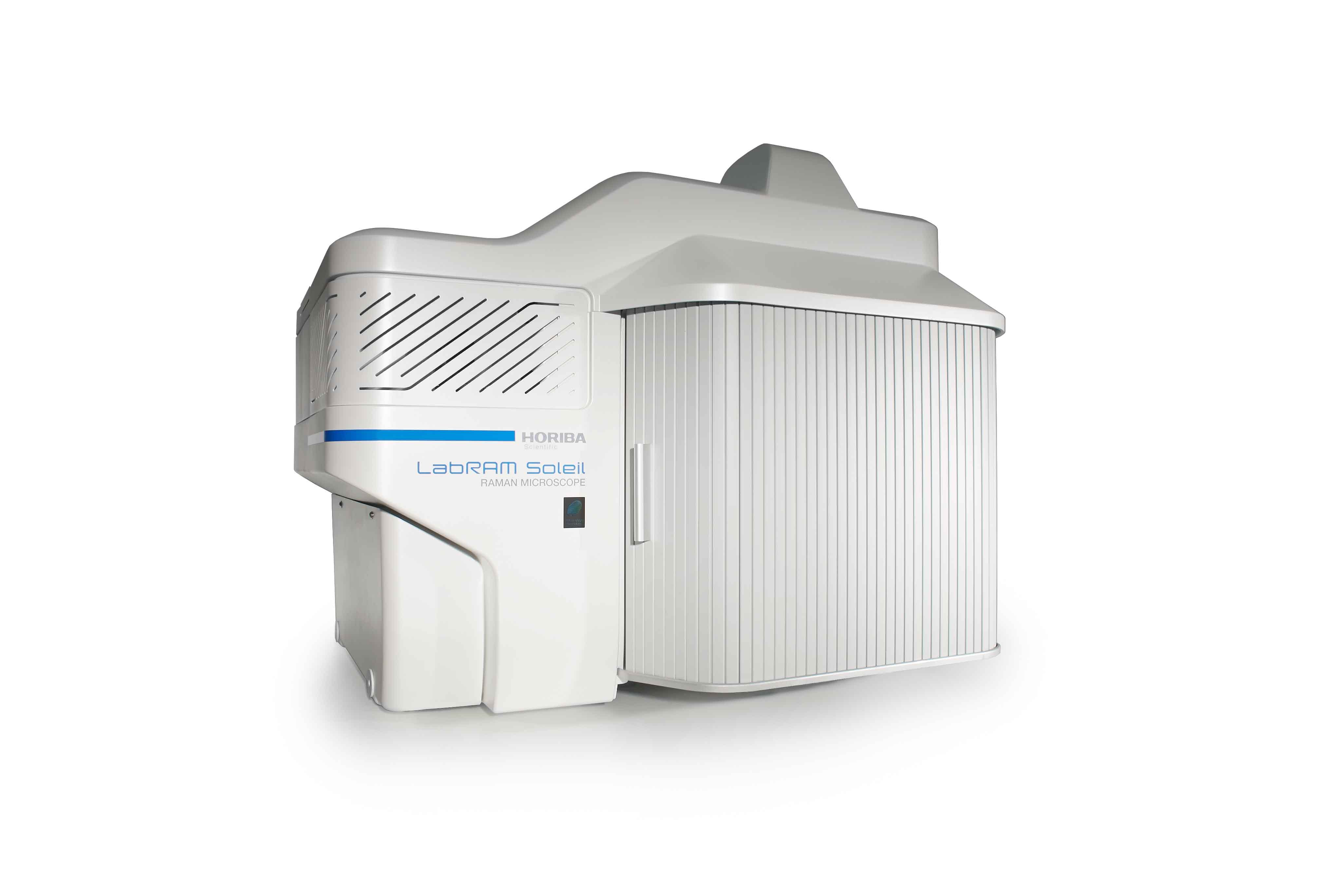
佳士科商贸有限公司为您提供《薄膜厚度的红外或近红外区域半导体晶片自动分析》,该方案主要用于其他中膜厚、检测,参考标准--,《薄膜厚度的红外或近红外区域半导体晶片自动分析》用到的仪器有JASCO傅立叶变换红外光谱仪FT/IR-6000、JASCONRS5000/7000共聚焦激光拉曼光谱仪、MSV-5000显微紫外可见近红外分光光度计、jasco紫外可见分光光度计 V-700
相关方案
更多
该厂商其他方案
更多