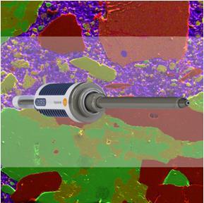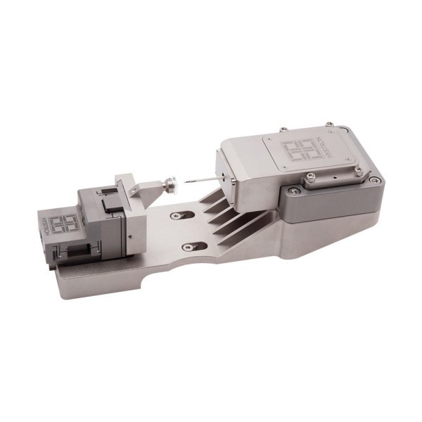
Using Bruker’s Hysitron PI 88 SEM PicoIndenter
equipped with tilt and rotation stages in conjunction with
the QUANTAX EBSD system enables a more robust
characterization of metallic materials by combining high
resolution phase and grain orientation mapping capabilities
with targeted nanomechanical property measurements.
This combination could also be used to extend the scope of
research related to other advanced textured, anisotropic, or
multi-phase materials.
方案详情

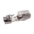
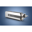
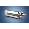
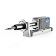
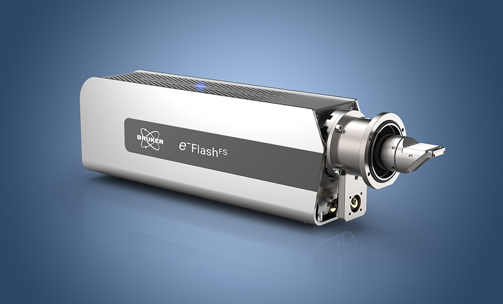
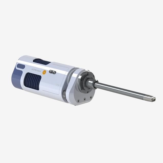
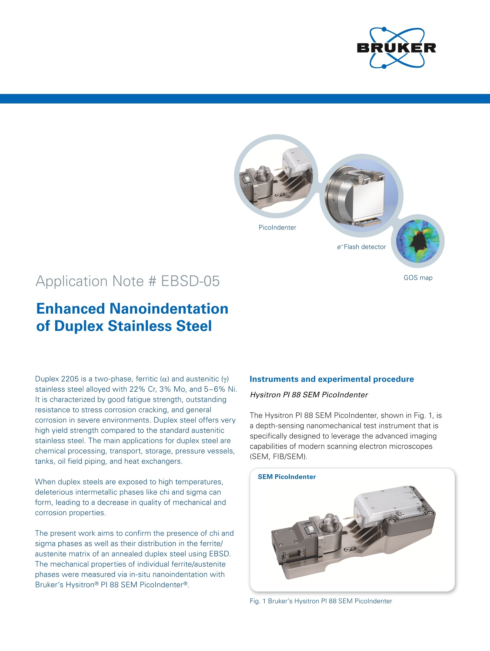
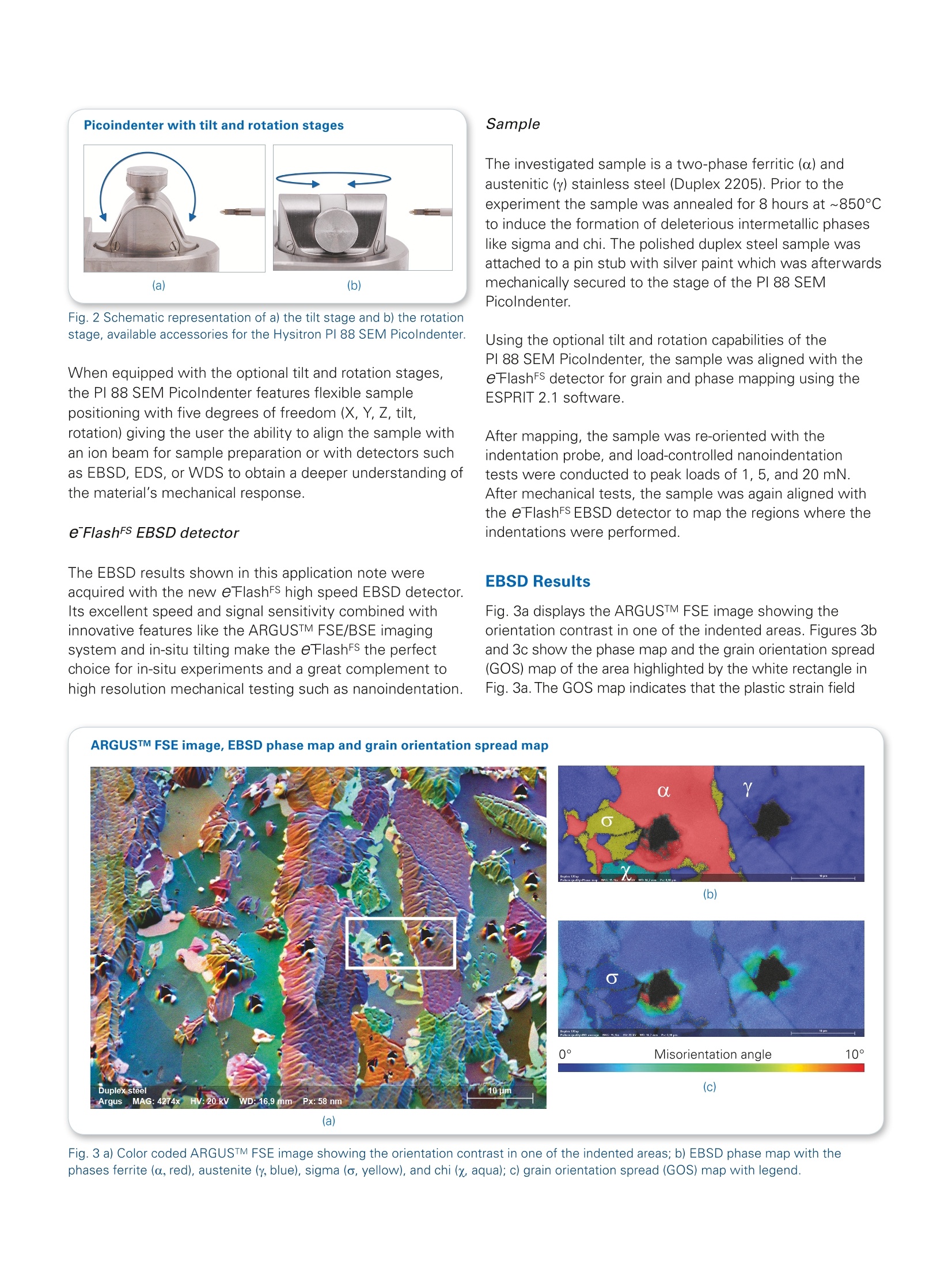
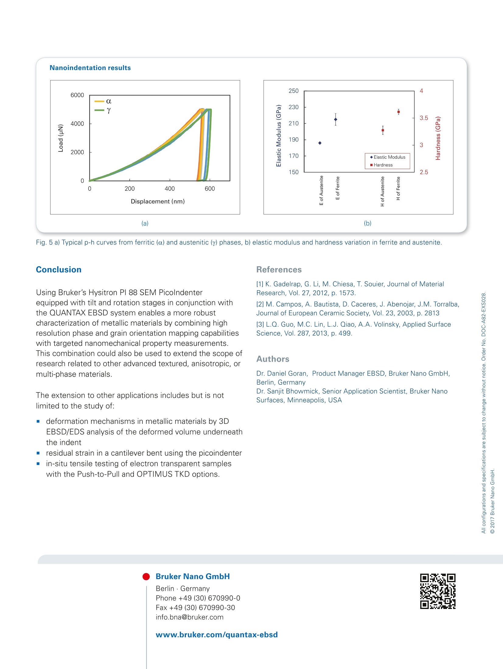
Berlin · Germany Application Note # EBSD-05 GOS map Enhanced Nanoindentationof Duplex Stainless Steel Duplex 2205 is a two-phase, ferritic (a) and austenitic (y)stainless steel alloyed with 22% Cr,3% Mo, and5-6% Ni.It is characterized by good fatigue strength, outstandingresistance to stress corrosion cracking, and generalcorrosion in severe environments. Duplex steel offers veryhigh yield strength compared to the standard austeniticstainless steel. The main applications for duplex steel arechemical processing, transport, storage, pressure vessels,tanks, oil field piping, and heat exchangers. Instruments and experimental procedure Hysitron PI 88 SEM Picolndenter The Hysitron PI 88 SEM Picolndenter, shown in Fig. 1, isa depth-sensing nanomechanical test instrument that isspecifically designed to leverage the advanced imagingcapabilities of modern scanning electron microscopes(SEM, FIB/SEM). When duplex steels are exposed to high temperatures,deleterious intermetallic phases like chi and sigma canform, leading to a decrease in quality of mechanical andcorrosion properties. The present work aims to confirm the presence of chi andsigma phases as well as their distribution in the ferrite/austenite matrix of an annealed duplex steel using EBSD.The mechanical properties of individual ferrite/austenitephases were measured via in-situ nanoindentation withBruker's Hysitron@ PI 88 SEM Picolndenter@. Fig. 1 Bruker's Hysitron PI 88 SEM Picolndenter Fig. 2 Schematic representation of a) the tilt stage and b) the rotationstage, available accessories for the Hysitron PI 88 SEM Picolndenter. When equipped with the optional tilt and rotation stages,the PI 88 SEM Picolndenter features flexible samplepositioning with five degrees of freedom (X,Y, Z, tilt,rotation) giving the user the ability to align the sample withan ion beam for sample preparation or with detectors suchas EBSD, EDS, or WDS to obtain a deeper understanding ofthe material's mechanical response. eFlashFS EBSD detector The EBSD results shown in this application note wereacquired with the new eFlashFs high speed EBSD detector.Its excellent speed and signal sensitivity combined withinnovative features like the ARGUSTM FSE/BSE imagingsystem and in-situ tilting make the eFlashFS the perfectchoice for in-situ experiments and a great complement tohigh resolution mechanical testing such as nanoindentation. The investigated sample is a two-phase ferritic (a) andaustenitic (y) stainless steel (Duplex 2205). Prior to theexperiment the sample was annealed for 8 hours at ~850°℃to induce the formation of deleterious intermetallic phaseslike sigma and chi. The polished duplex steel sample wasattached to a pin stub with silver paint which was afterwardsmechanically secured to the stage of the PI 88 SEMPicolndenter. Using the optional tilt and rotation capabilities of thePI 88 SEM Picolndenter, the sample was aligned with theeFlashFS detector for grain and phase mapping using theESPRIT 2.1 software. After mapping, the sample was re-oriented with theindentation probe,and load-controlled nanoindentationtests were conducted to peak loads of 1, 5, and 20 mN.After mechanical tests, the sample was again aligned withthe eFlashFS EBSD detector to map the regions where theindentations were performed. EBSD Results Fig. 3a displays the ARGUSTM FSE image showing theorientation contrast in one of the indented areas. Figures 3band 3c show the phase map and the grain orientation spread(GOS) map of the area highlighted by the white rectangle inFig. 3a. The GOS map indicates that the plastic strain field Fig.3 a) Color coded ARGUSTM FSE image showing the orientation contrast in one of the indented areas; b) EBSD phase map with thephases ferrite (a, red), austenite(y, blue), sigma (o, yellow), and chi (x, aqua); c) grain orientation spread (GOS) map with legend. Fig. 4 a) Pattern quality map; b) phase map; c) orientation map (IPFy), d) GOS map. The colors in d) indicate the orientation spread in degreesfrom0° (blue) up to 15°(red). developed by the indent does not cross from the ferrite graininto the much harder sigma phase grain. Fig.4 shows the EBSD results acquired from an areacontaining an indent made at the boundary between aferrite (a) grain and an austenite (y) grain. The resultsindicate that the amount of plastic deformation induced bythe indent is much larger in the austenite, i.e. the softerphase. EBSD-Enhanced Nanoindentation Results The local elastic and plastic properties of the phasedomains were determined from load-displacement curves by analyzing five to eight indentations from each phase(Fig.5a). The elastic moduli (E) were measured to be 215± 7.2 GPa and 186±1.4 GPa for the ferritic and austeniticphases, respectively (Fig.5b). The hardness values (H) show a similar trend with values of3.6±0.05 GPa for ferrite and 3.2±0.07 GPa for austenite(Fig. 5b). Although the actual numbers vary slightly from theresults reported by Gadelrab et al., Campos et al., and Guoet al.,the relative difference in the mechanical properties ofthe two phases agrees well with the trends reported in theprevious studies. Also, the results confirm the expected enhancement providedby solid solution hardening of Ni and Mo in the ferrite phase. [1]K. Gadelrap,G. Li, M. Chiesa, T. Souier, Journal of MaterialResearch, Vol. 27,2012, p. 1573. Using Bruker’s Hysitron PI 88 SEM Picolndenterequipped with tilt and rotation stages in conjunction withthe QUANTAX EBSD system enables a more robustcharacterization of metallic materials by combining highresolution phase and grain orientation mapping capabilitieswith targeted nanomechanical property measurements.This combination could also be used to extend the scope ofresearch related to other advanced textured, anisotropic, ormulti-phase materials. [2] M. Campos, A. Bautista, D. Caceres, J. Abenojar, J.M. Torralba,Journal of European Ceramic Society, Vol. 23,2003, p. 2813 [3] L.Q. Guo, M.C. Lin, L.J. Qiao, A.A. Volinsky, Applied SurfaceScience, Vol. 287, 2013, p. 499. Authors Dr. Daniel Goran, Product Manager EBSD, Bruker Nano GmbH,Berlin, Germany The extension to other applications includes but is notlimited to the study of: Dr. Sanjit Bhowmick, Senior Application Scientist, Bruker NanoSurfaces, Minneapolis, USA deformation mechanisms in metallic materials by 3DEBSD/EDS analysis of the deformed volume underneaththe indent residual strain in a cantilever bent using the picoindenter in-situ tensile testing of electron transparent sampleswith the Push-to-Pull and OPTIMUS TKD options. Bruker Nano GmbH Phone +49 (30)670990-0 Fax +49 (30)670990-30 info.bna@bruker.com www.bruker.com/quantax-ebsd Using Bruker’s Hysitron PI 88 SEM PicoIndenterequipped with tilt and rotation stages in conjunction withthe QUANTAX EBSD system enables a more robustcharacterization of metallic materials by combining highresolution phase and grain orientation mapping capabilitieswith targeted nanomechanical property measurements.This combination could also be used to extend the scope ofresearch related to other advanced textured, anisotropic, ormulti-phase materials.
确定

还剩2页未读,是否继续阅读?
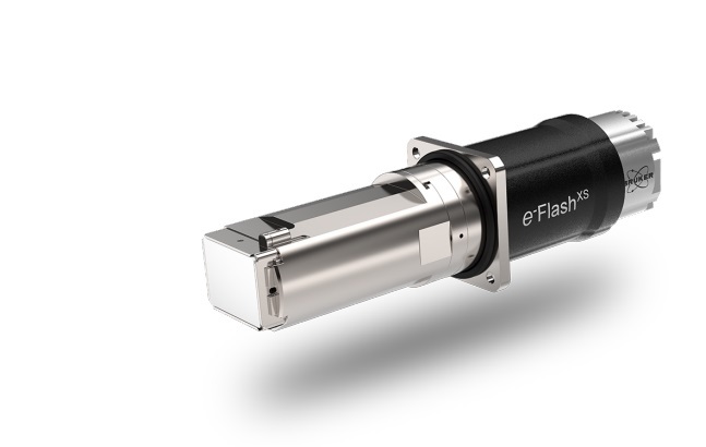
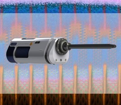
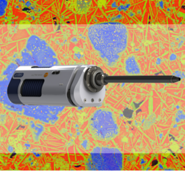
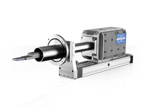
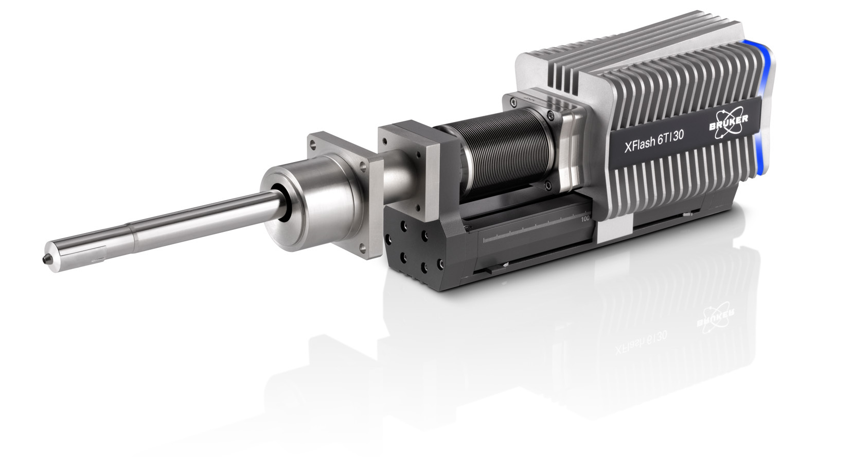
布鲁克电子显微纳米分析仪器部为您提供《不锈钢中元素含量检测方案(电镜部件)》,该方案主要用于粗钢中含量分析检测,参考标准--,《不锈钢中元素含量检测方案(电镜部件)》用到的仪器有布鲁克扫描电镜专用原位纳米力学测试系统PI 88、布鲁克 电子背散射衍射仪 EBSD eflash FS、布鲁克 电子背散射衍射仪 EBSD、布鲁克 平插式能谱仪FlatQUAD
推荐专场
电子背散射衍射系统(EBSD)
更多
相关方案
更多


