


锂电池材料从生产到检测、分析的整体思路,具有重要参考意义。
包括三方面:
1)微区表面形貌观察及分析
2)化学分析
3)制造
方案详情

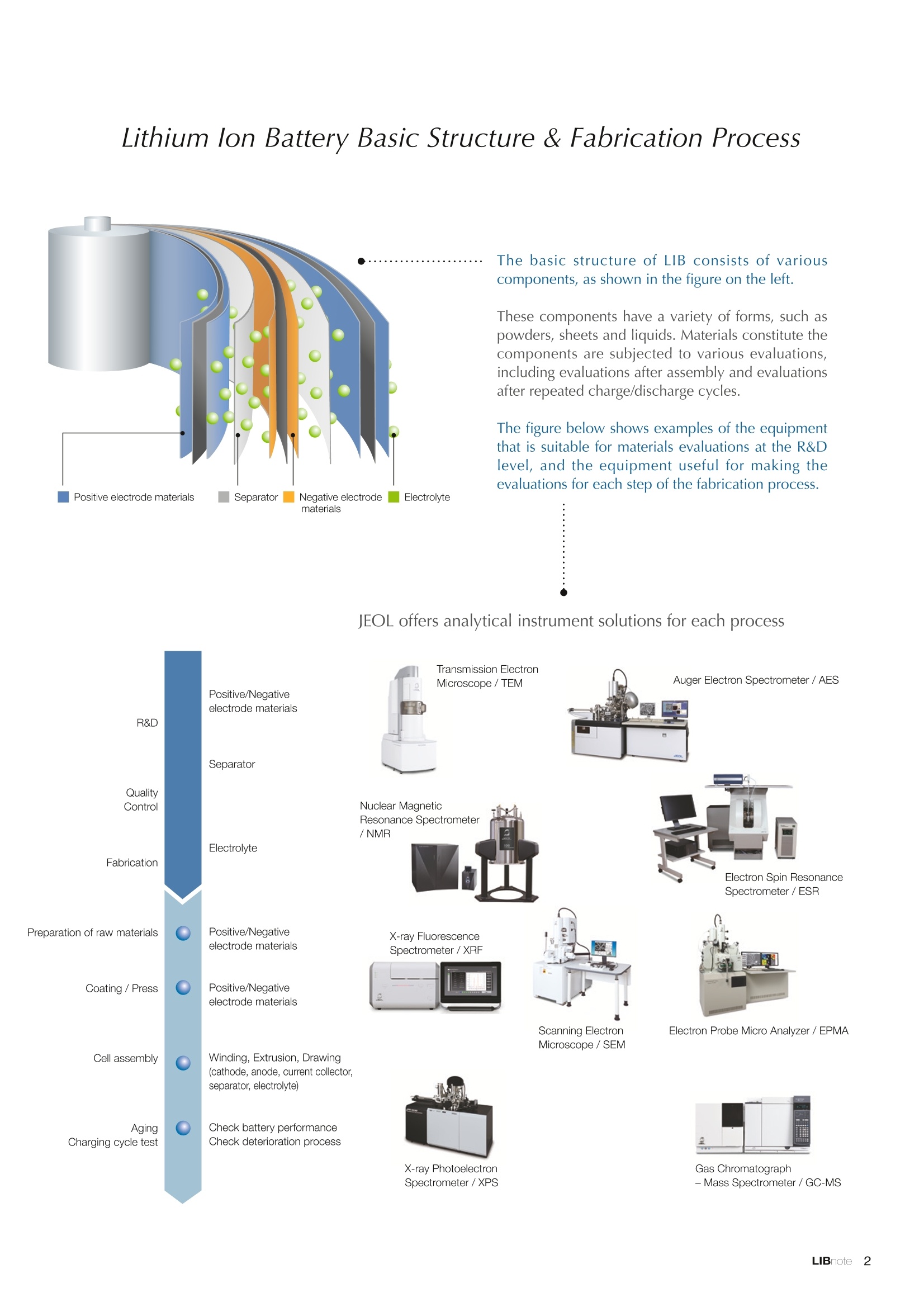
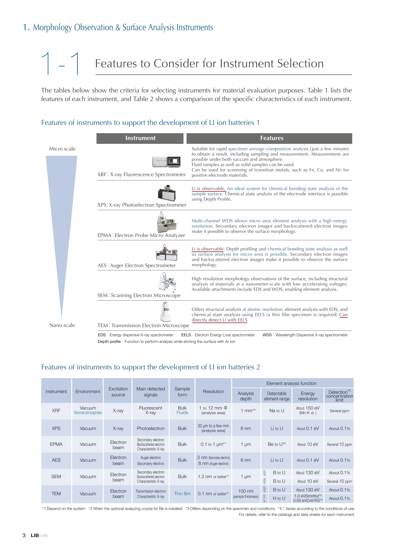
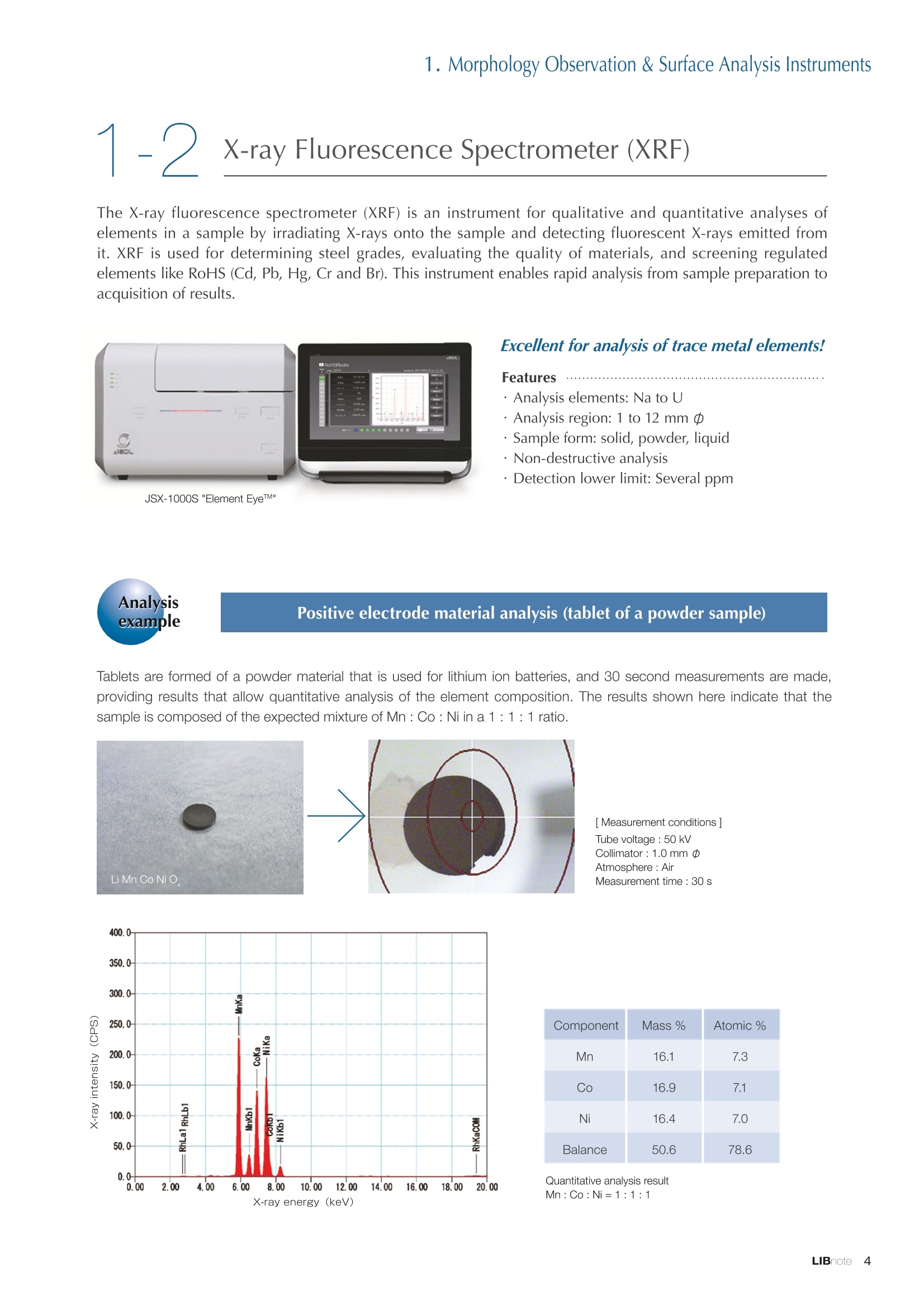
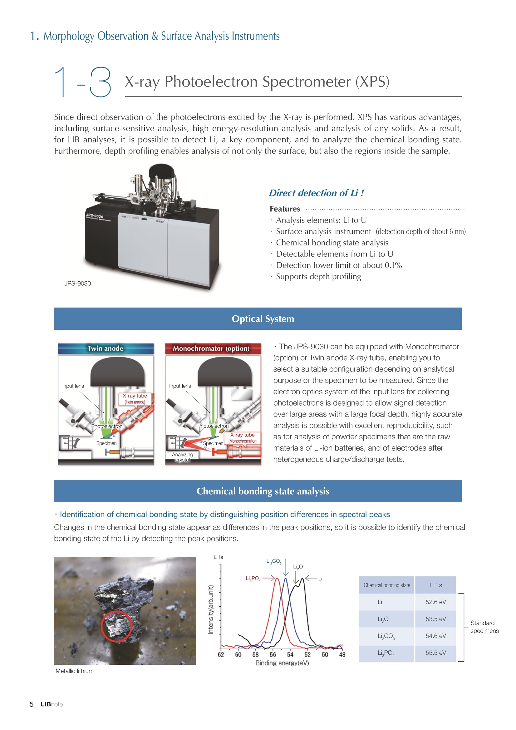
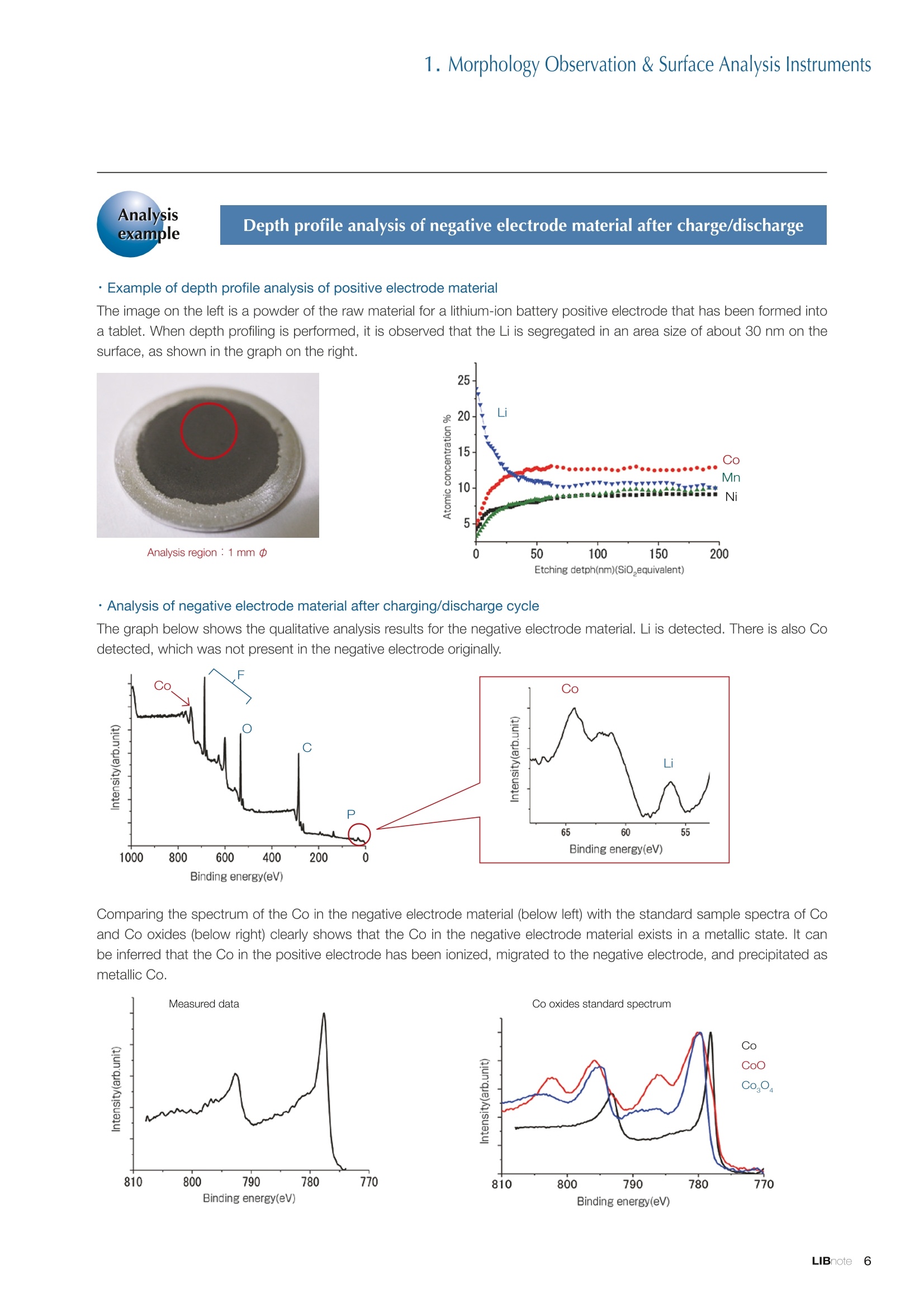
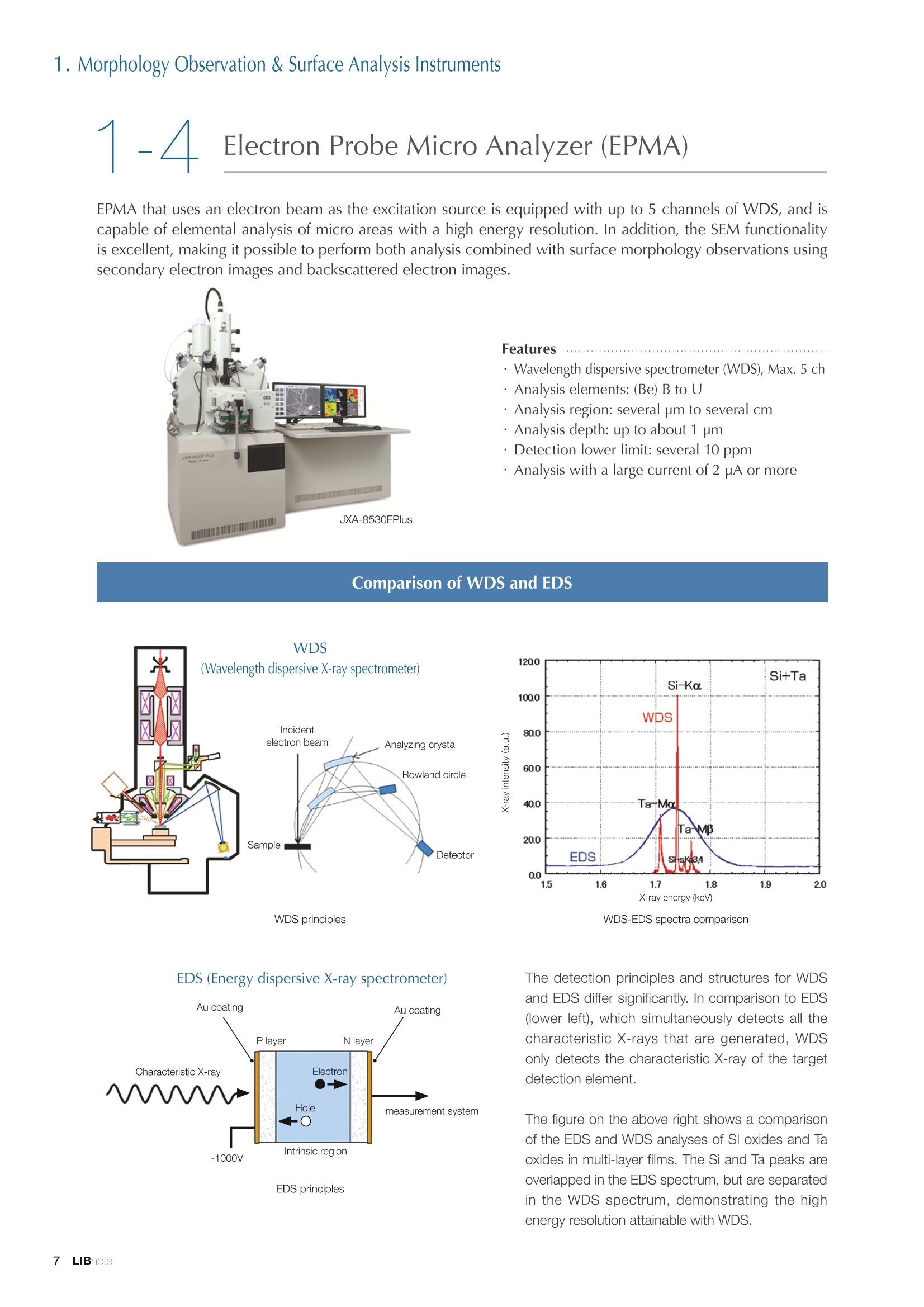
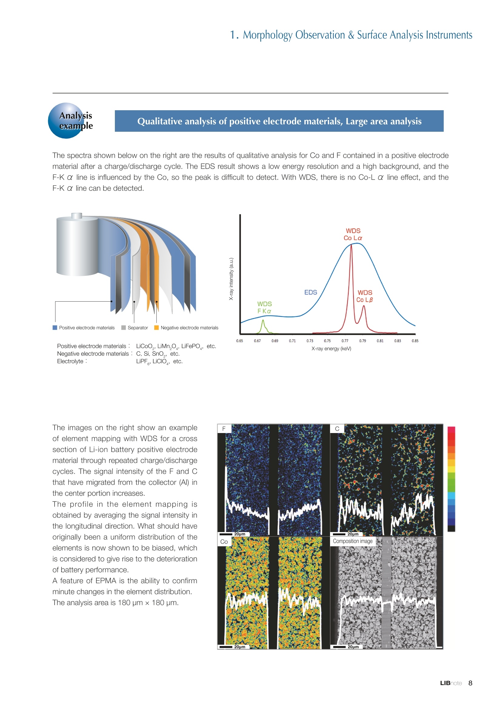
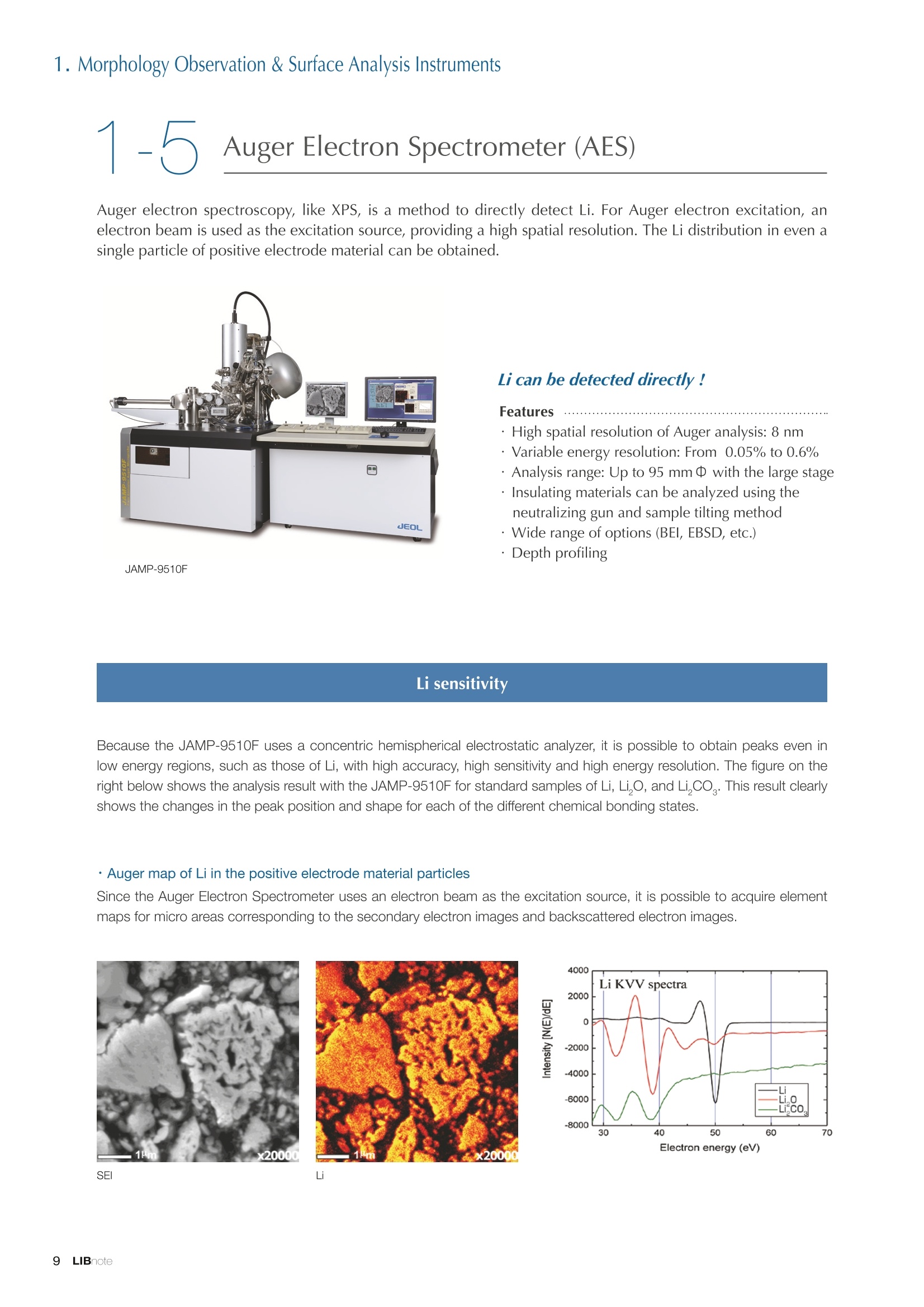
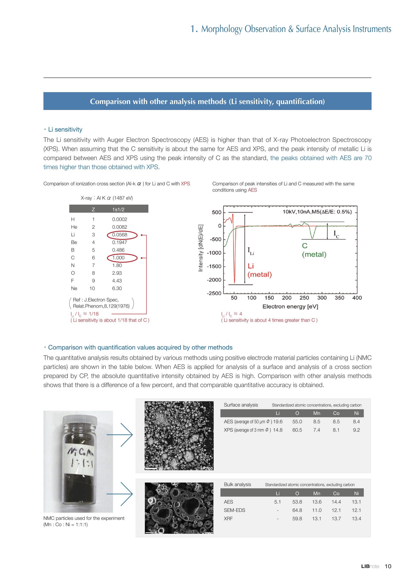
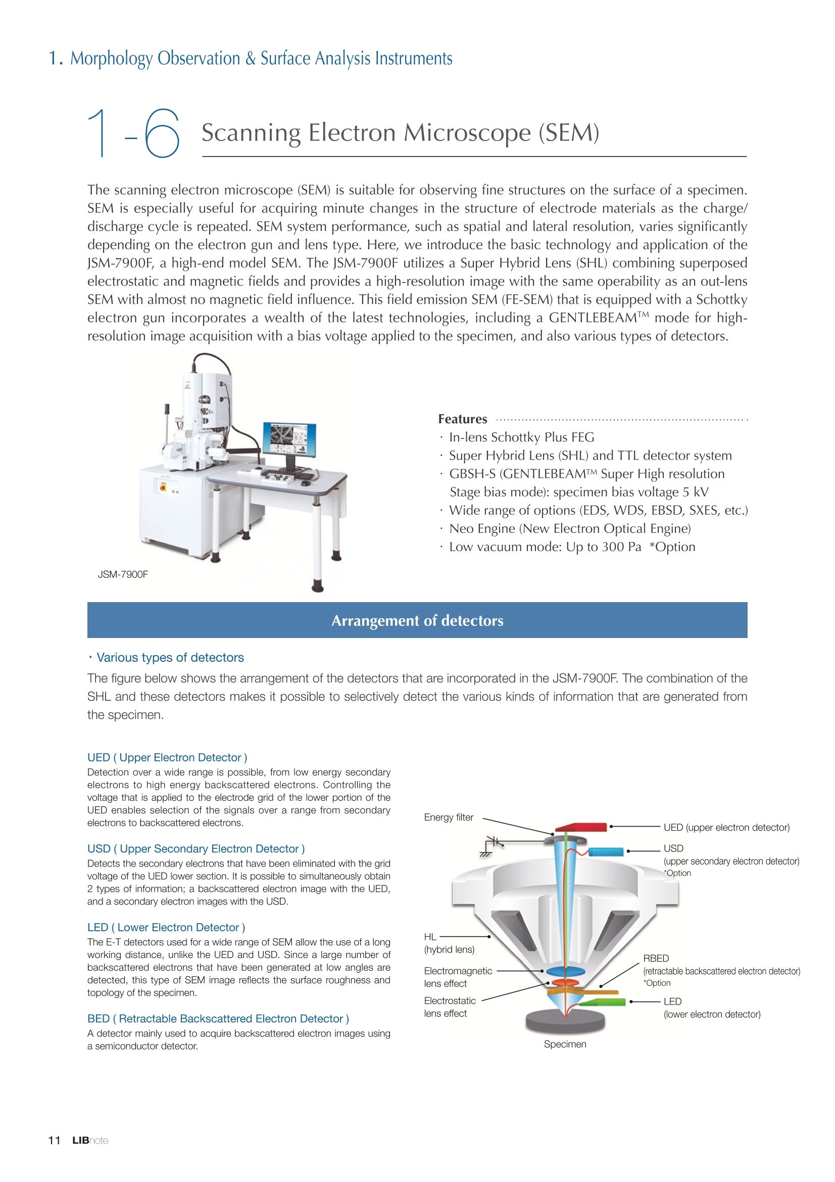
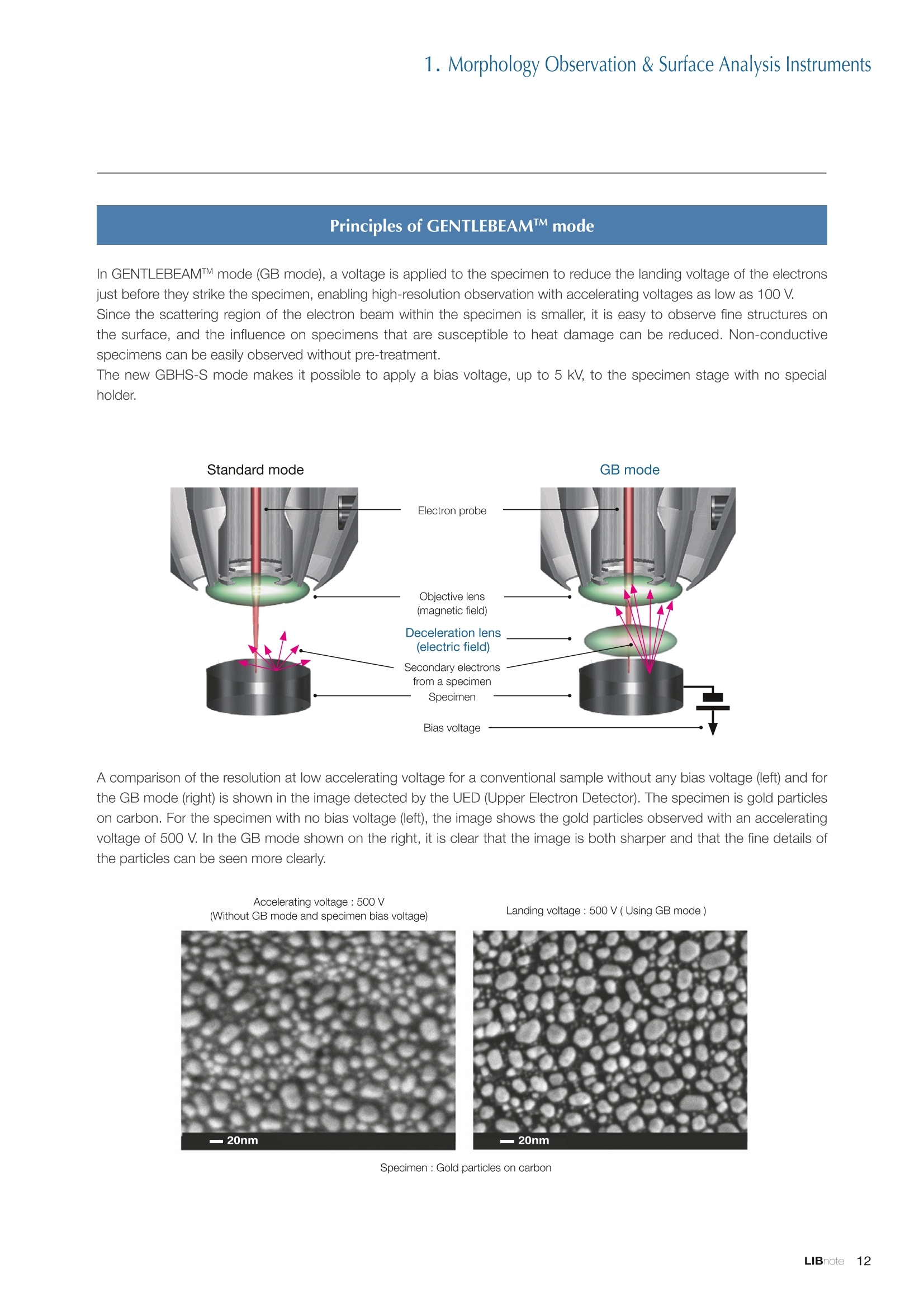
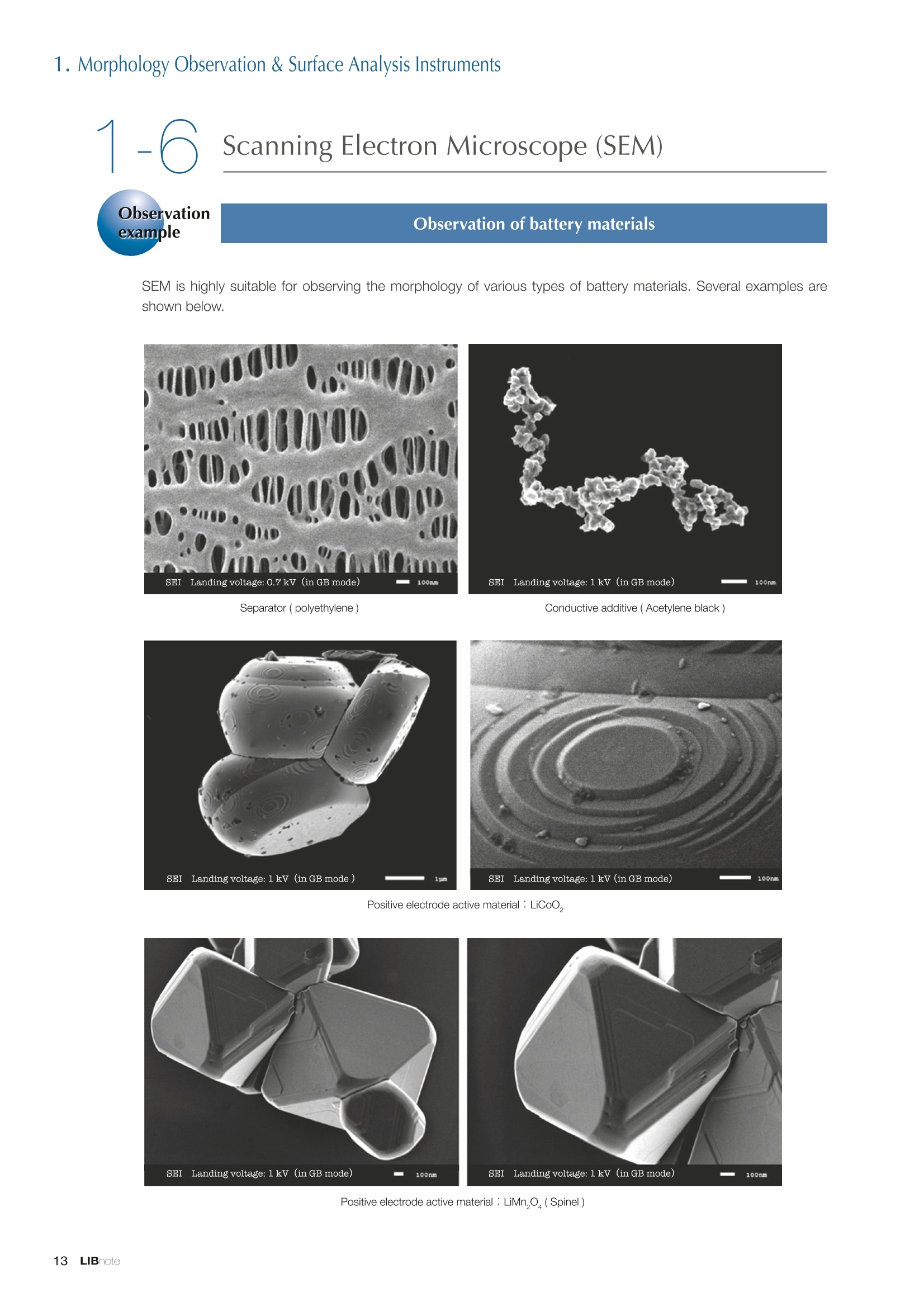
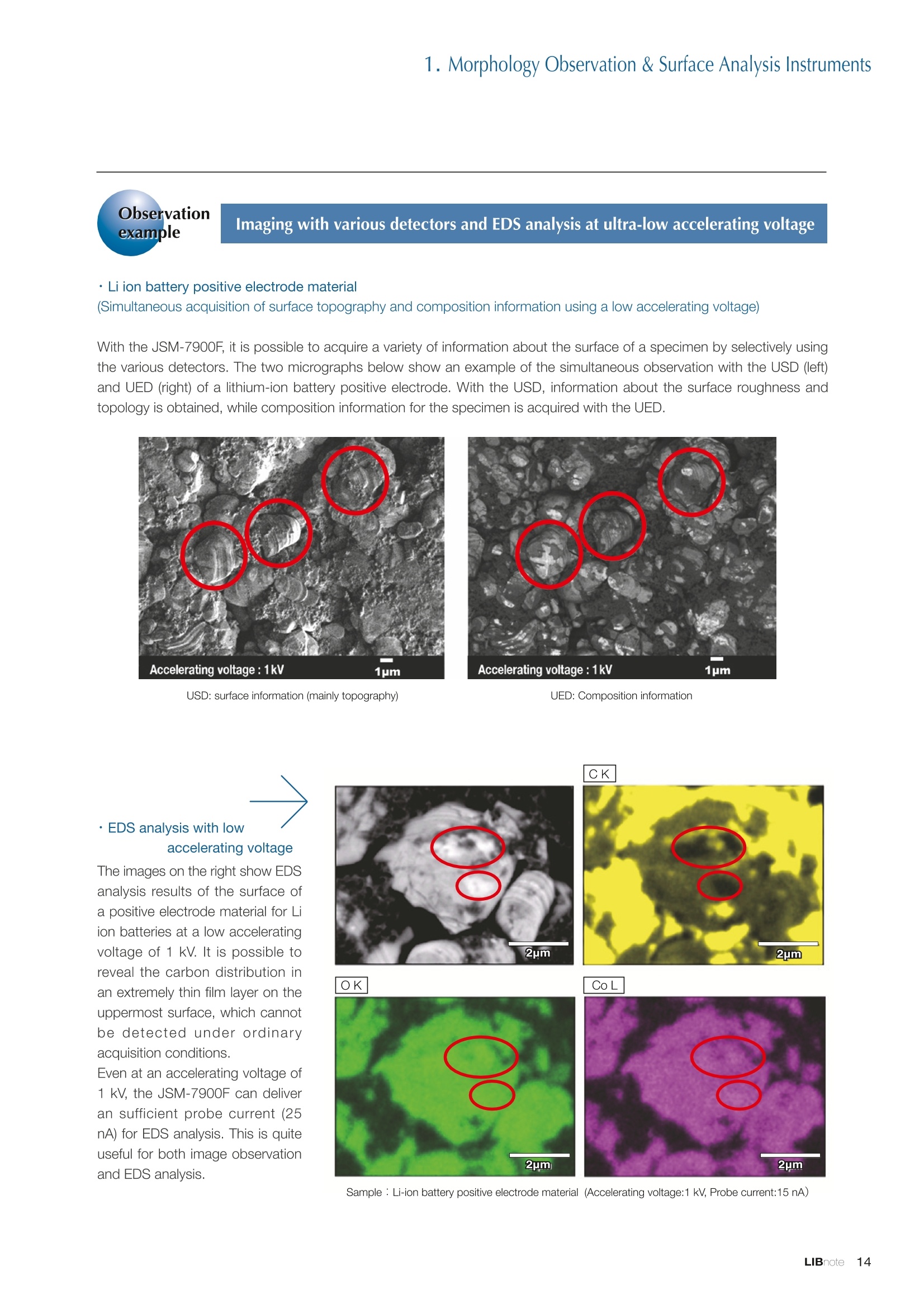
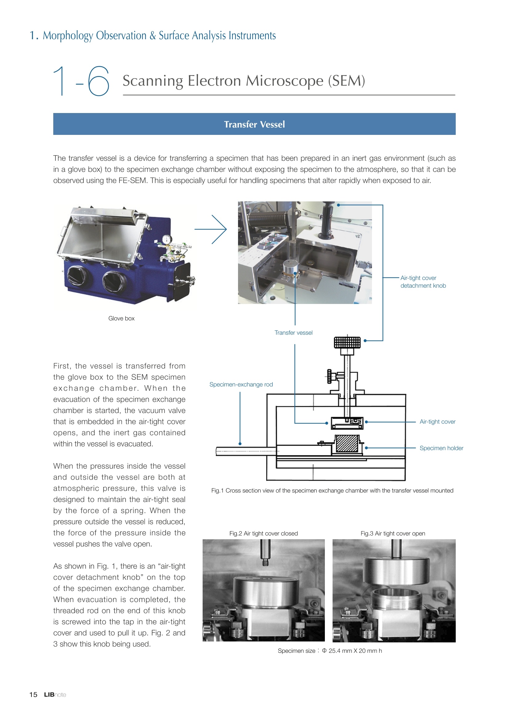
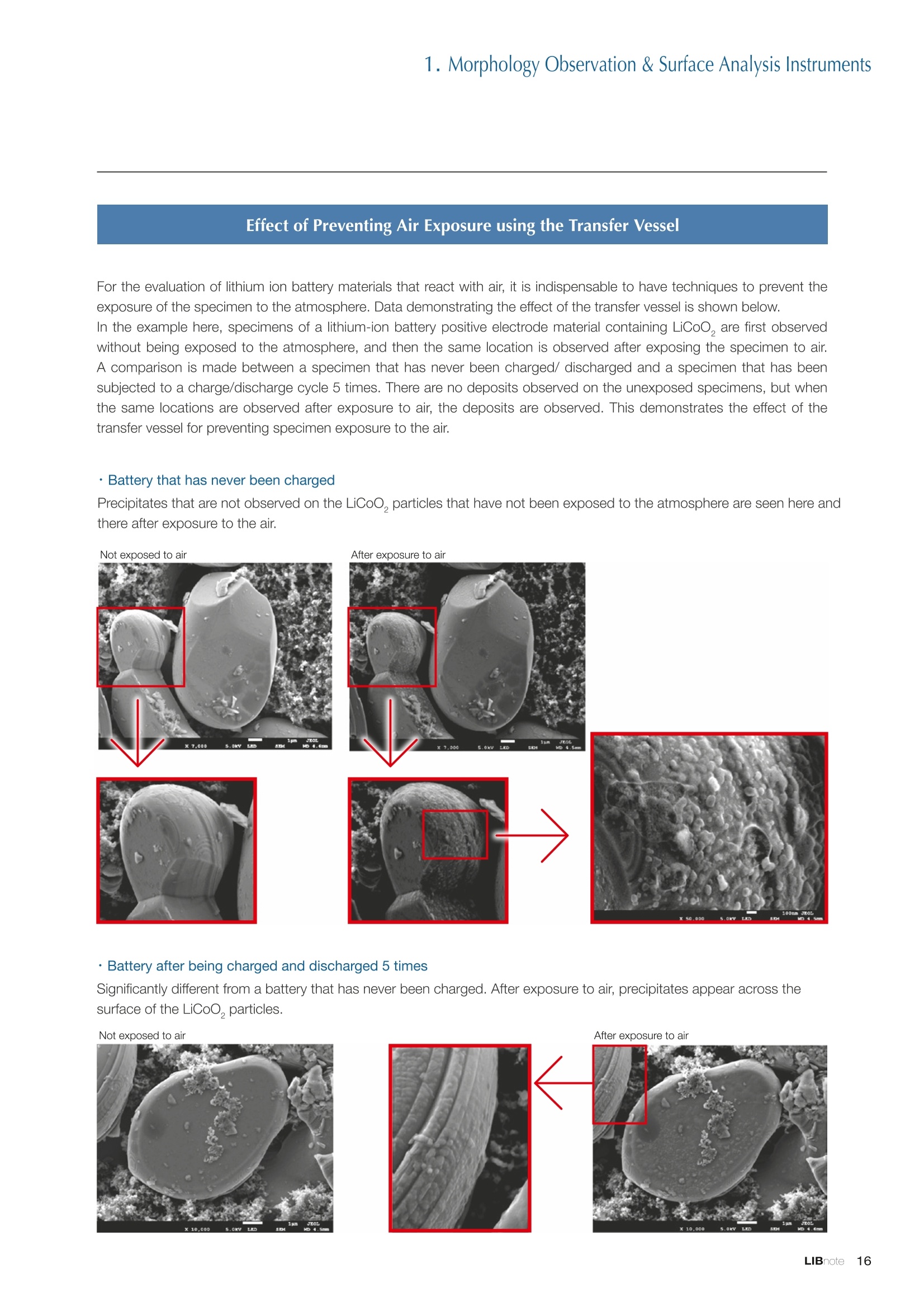
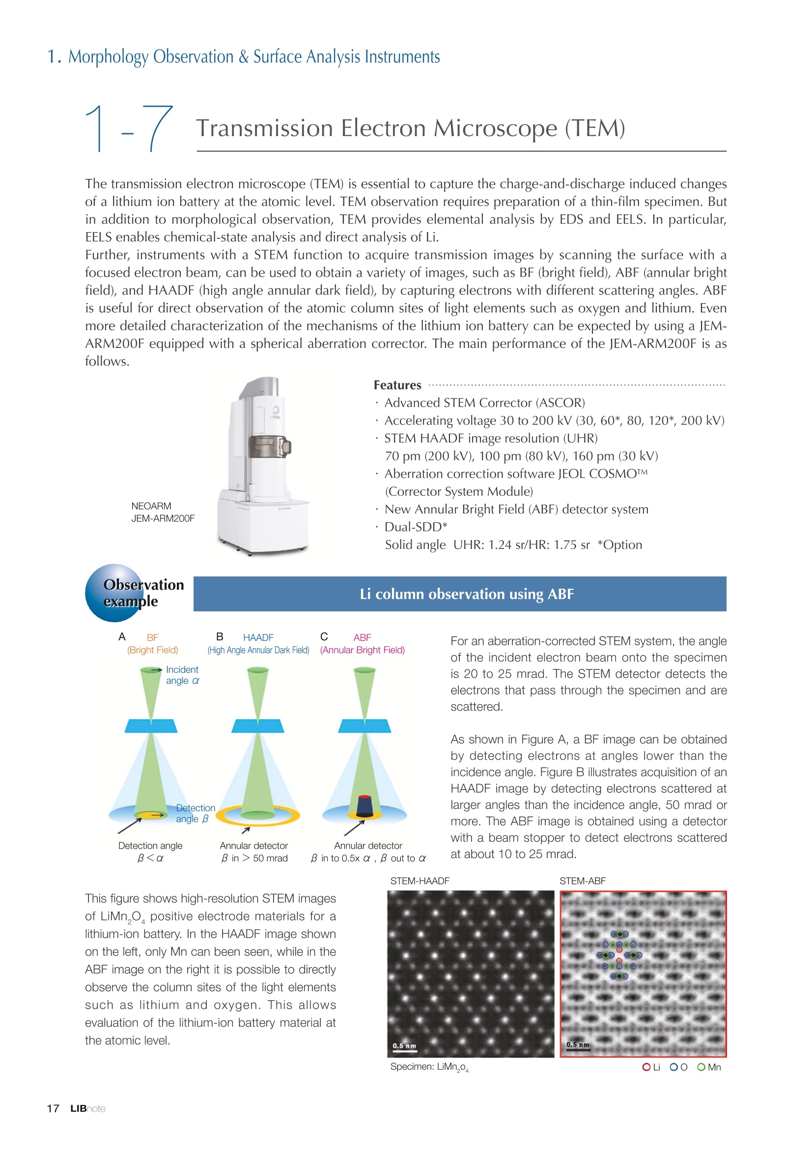
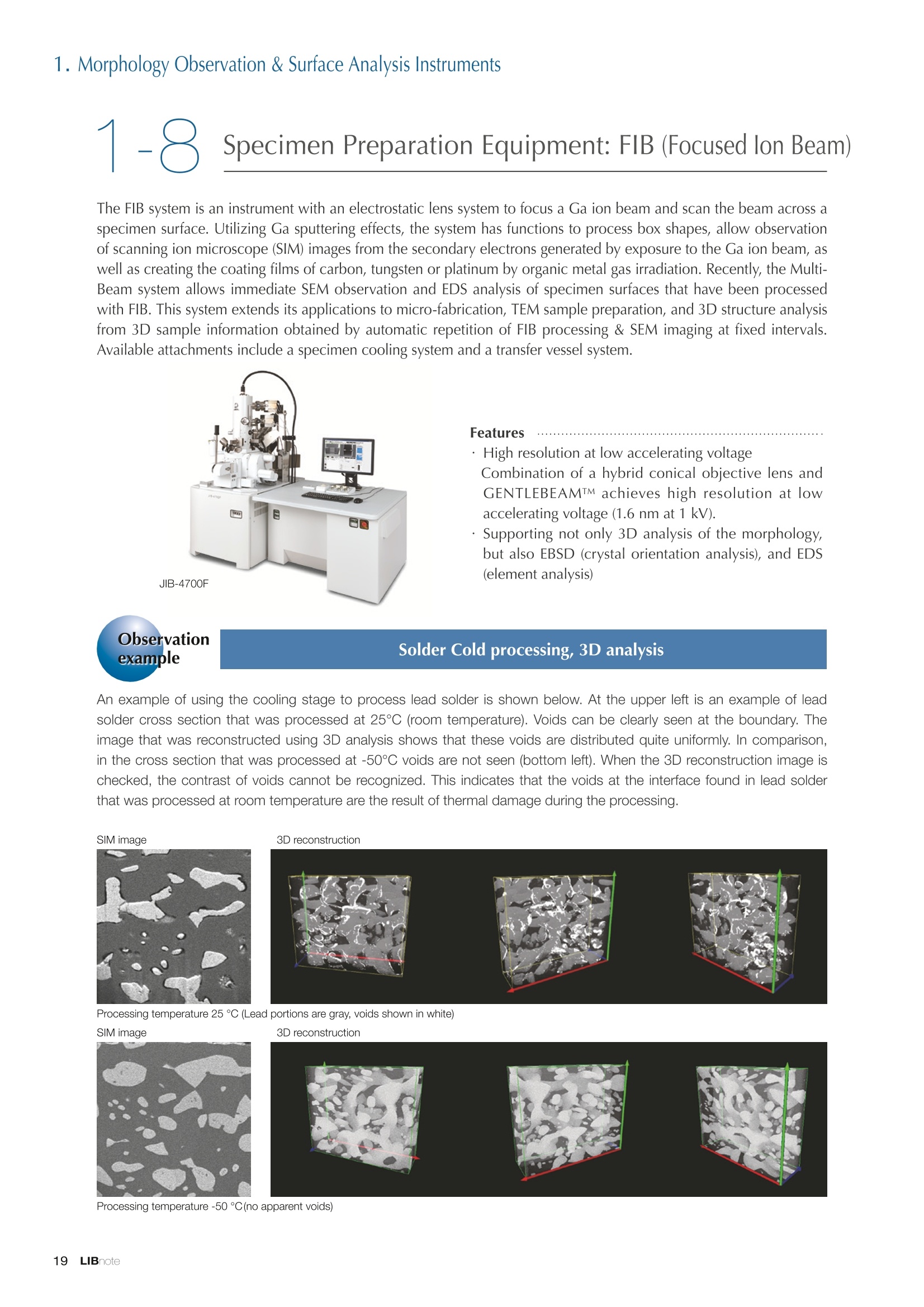
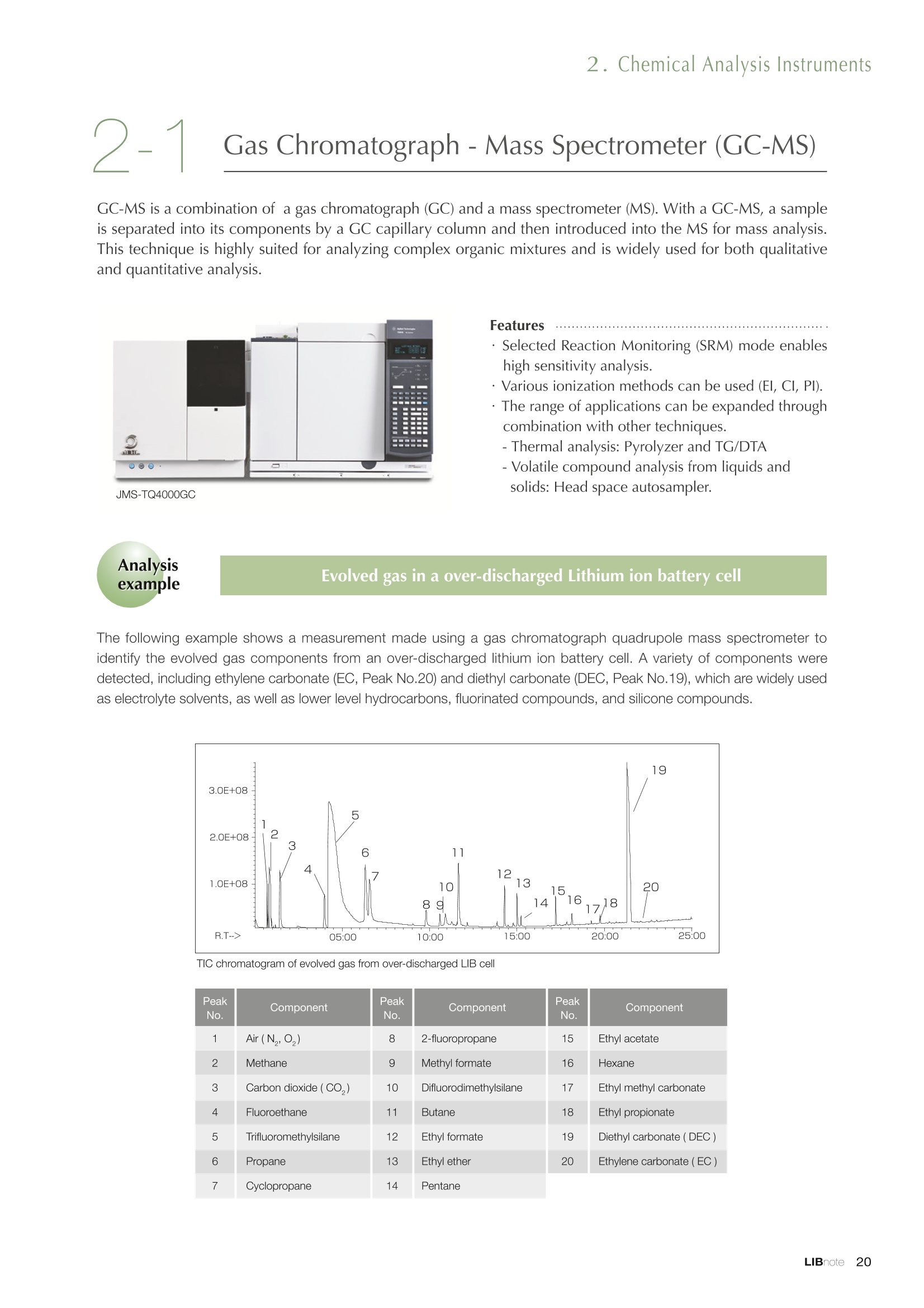
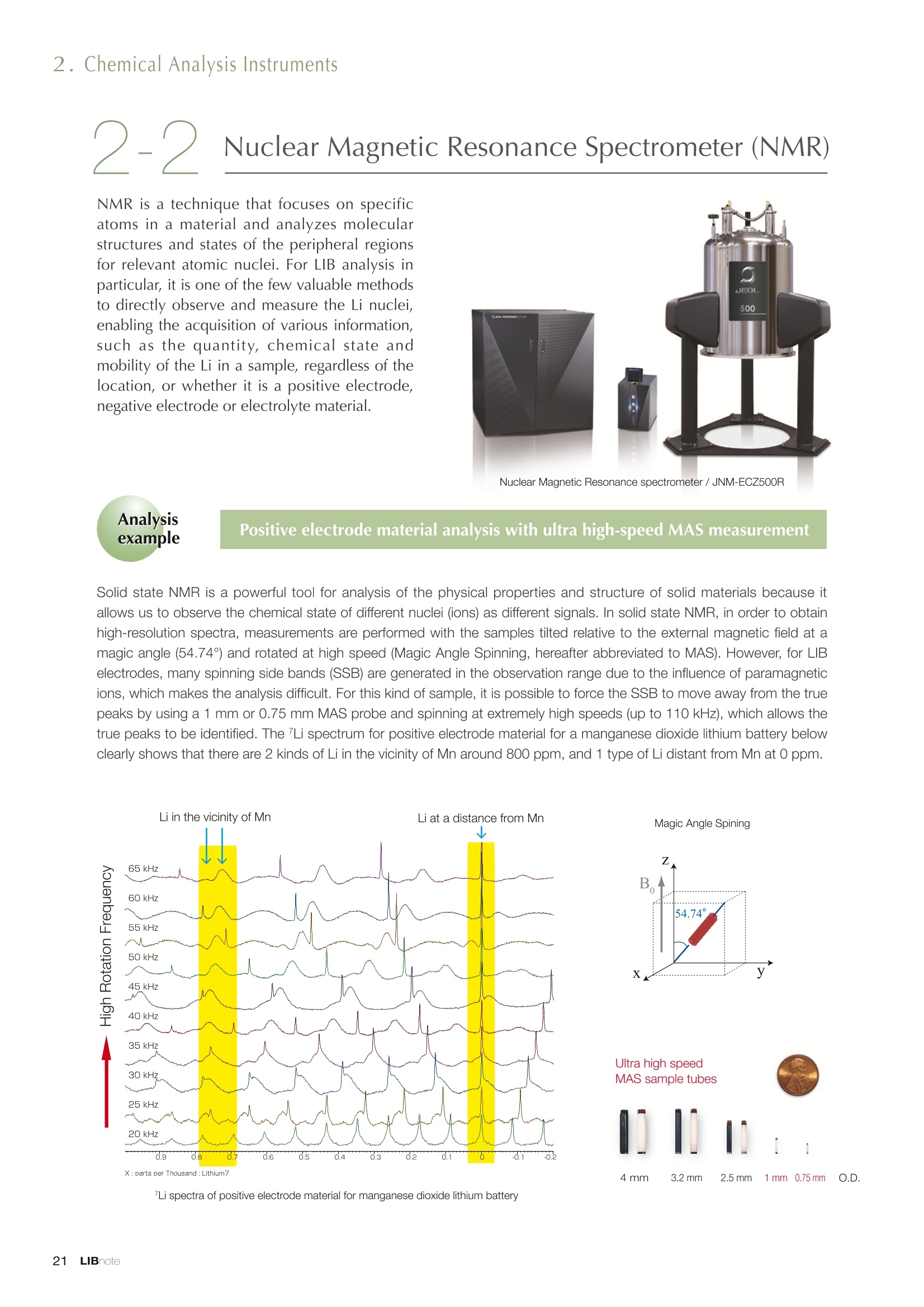
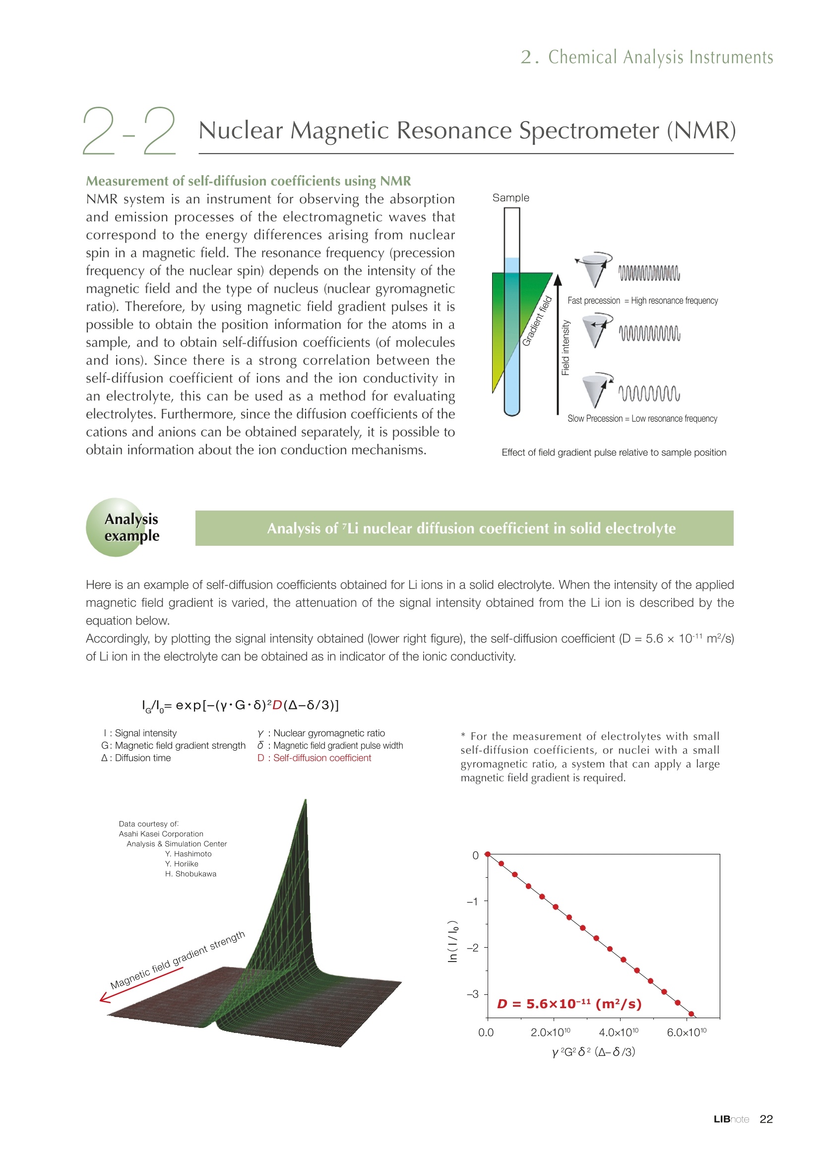
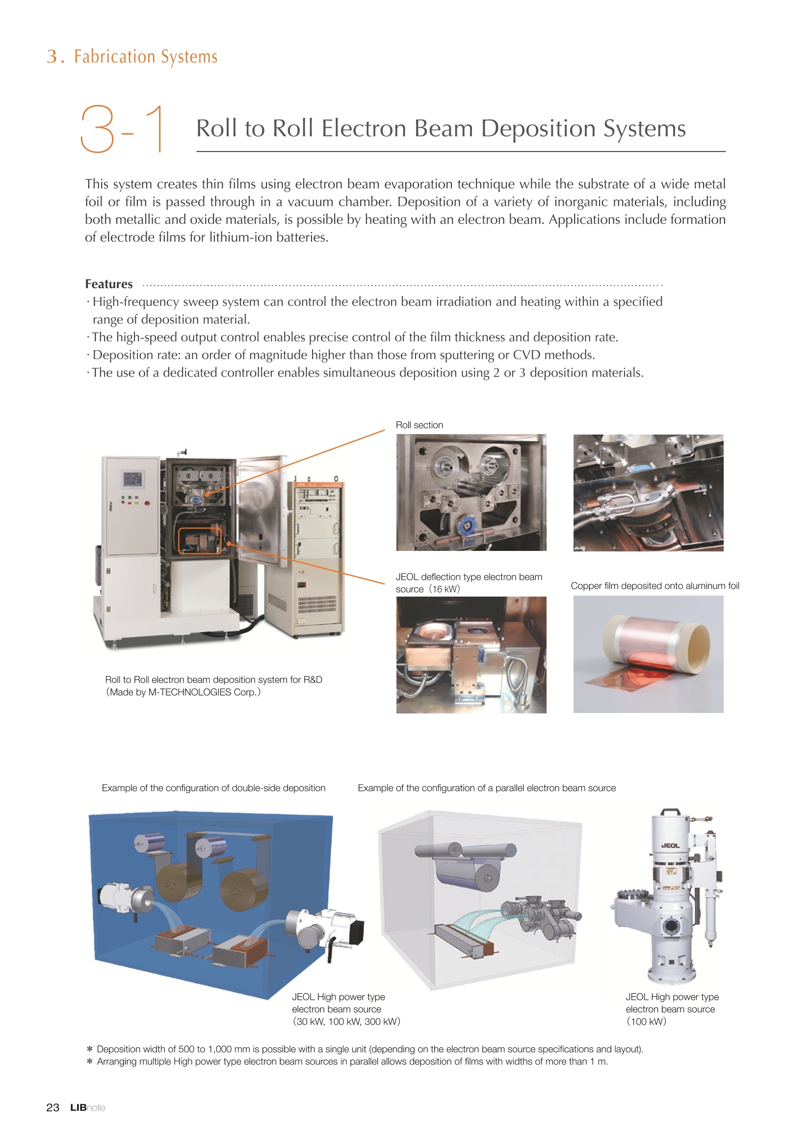
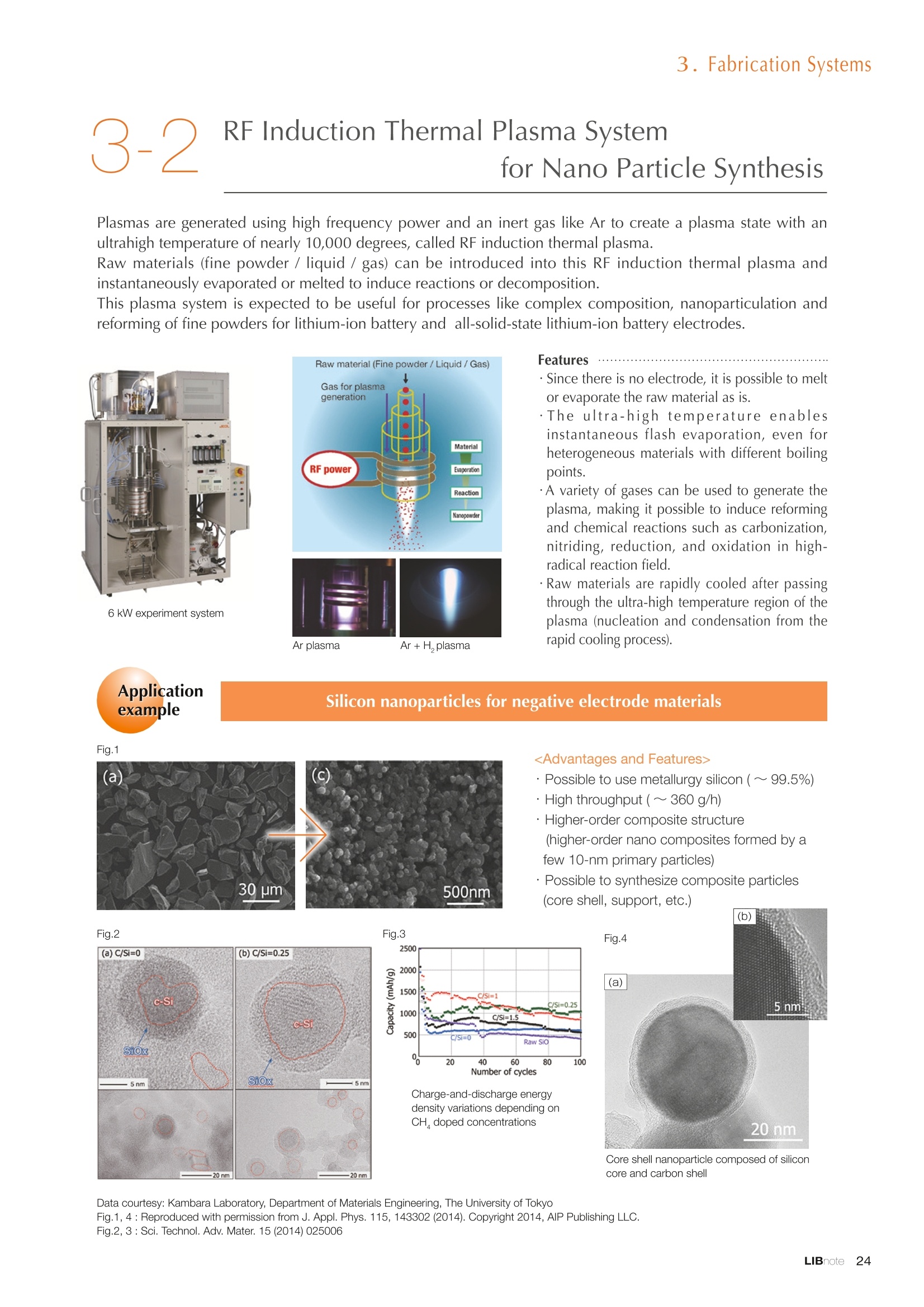
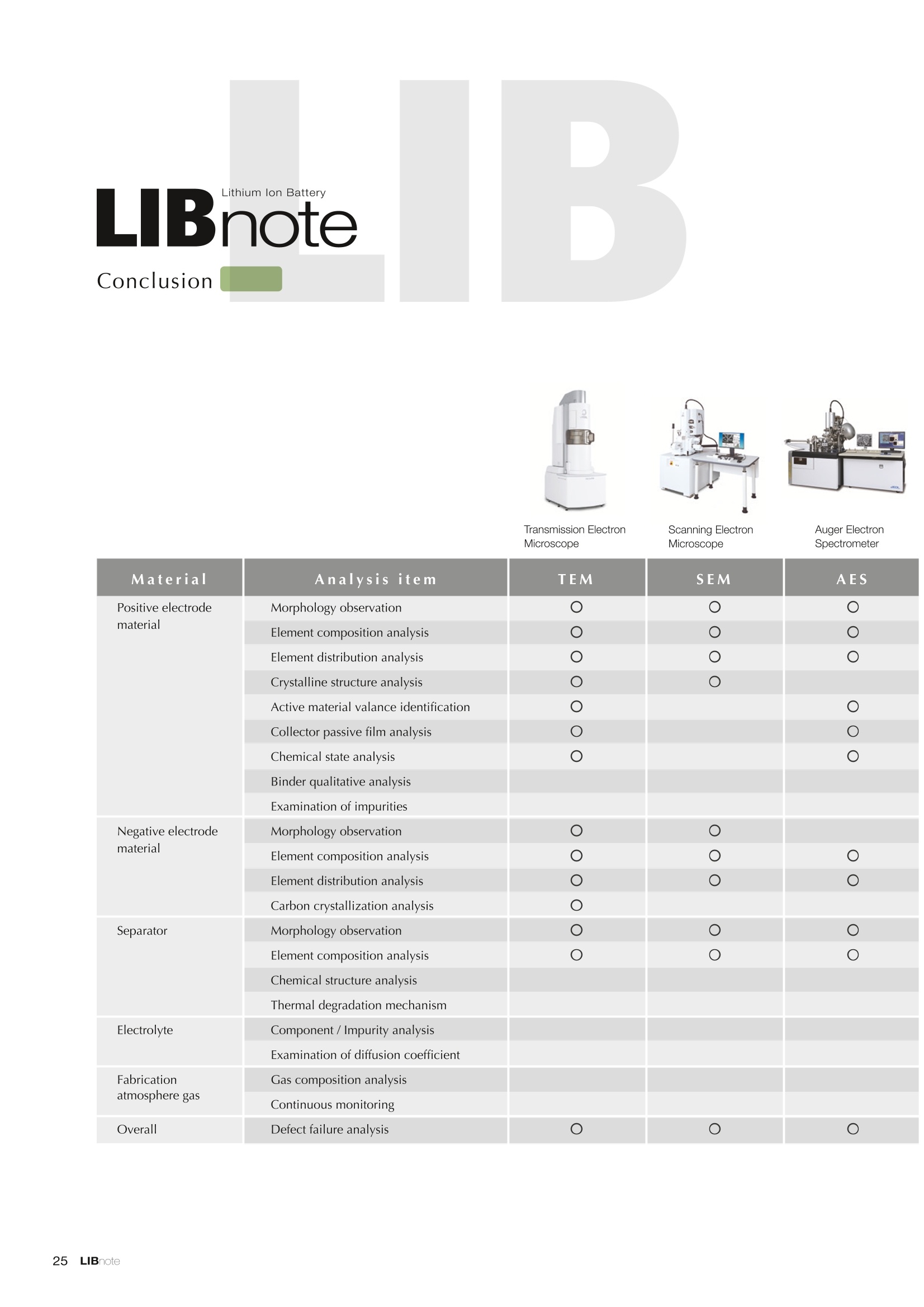
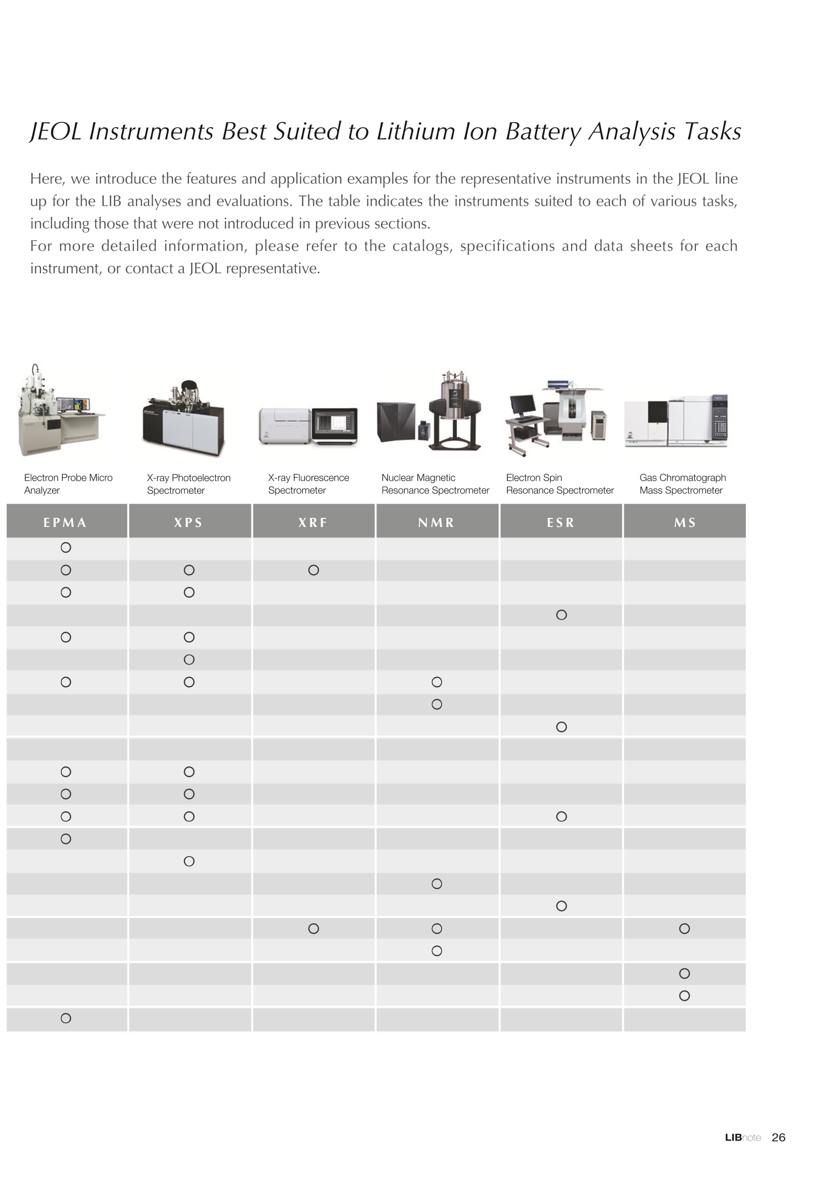
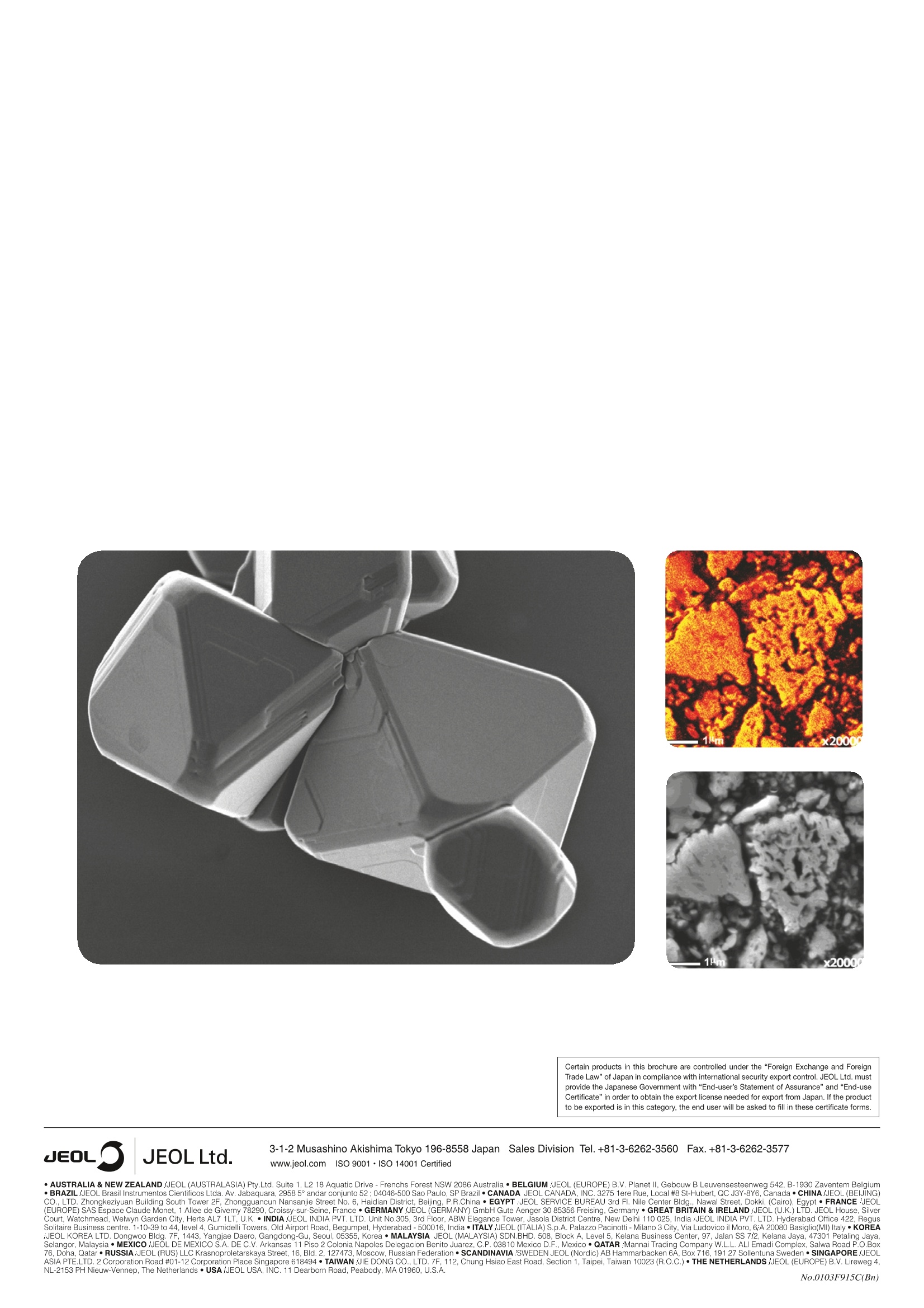
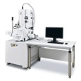
Applications noteLithium lon Battery note 1. Morphology Observation & Surface Analysis Instruments Morphology Observation & Surface Analysis InstrumentsXRF/XPS/EPMA/AES/SEM/TEM/CP/FIB Chemical Analysis InstrumentsGC-MS/NMR Fabrication Systems Roll to Roll Electron Beam Deposition SystemsRF Induction Thermal Plasma System for Nano Particle Synthesis JEOL Ltd. Introduction The applications for lithium ion batteries (LIB) cover a wide range of fields, from power sources for computersand mobile devices to automobiles. In this context, demands are increasingly accelerated for higherperformance (battery output, stability,etc.) and higher safety of batteries. In order to improve the performanceand quality of LIB, analysis and evaluation that combine various high-performance evaluation systems arerequired. JEOL offers a full line-up of equipment to support the development of new LIB technologies and toimprove product quality, including morphological observation instruments at the micrometer to nanometerscale, surface analysis instruments and chemical analysis systems to create high-performance coatings andpowders. This LIB note offers solutions for researchers and engineers who are looking for the best equipmentfor their applications. INDEX Introduction P01 Lithium Ion Battery Basic Structure & Fabrication Process P02 1.Morphology Observation & Surface Analysis Instruments 1-1. Features to Consider for Instrument Selection P03 1-2. XRF: X-ray Fluorescence Spectrometer P04 1-3.XPS: X-ray Photoelectron Spectrometer P05 1-4. EPMA: Electron Probe Micro Analyzer P07 1-5.AES: Auger Electron Spectrometer P09 1-6. SEM: Scanning Electron Microscope P11 1-7.TEM: Transmission Electron Microscope P17 1-8. CP: Specimen Preparation Equipment: Air Isolation & Cooling CP,FIB P18 2.Chemical Analysis Instruments 2-1. GC-MS: Gas Chromatograph Mass Spectrometer P20 2-2.NMR: Nuclear Magnetic Resonance Spectrometer P21 3.Fabrication Systems 3-1. Roll to Roll Electron Beam Deposition Systems P23 3-2.RF Induction Thermal Plasma System for Nano Particle Synthesis P24 Conclusion Analysis Items and Applicable Instruments P25 Lithium lon Battery Basic Structure & Fabrication Process The basic structure of LIB consists of variouscomponents, as shown in the figure on the left. These components have a variety of forms, such aspowders, sheets and liquids. Materials constitute thecomponents are subjected to various evaluations,including evaluations after assembly and evaluationsafter repeated charge/discharge cycles. The figure below shows examples of the equipmentthat is suitable for materials evaluations at the R&Dlevel, and the equipment useful for making theevaluations for each step of the fabrication process. 1-1Features to Consider for Instrument Selection The tables below show the criteria for selecting instruments for material evaluation purposes. Table 1 lists thefeatures of each instrument, and Table 2 shows a comparison of the specific characteristics of each instrument. Features of instruments to support the development of Ll ion batteries 1 Instrument Features Suitable for rapid specimen average composition analysis (just a few minutes XRF : X-ray Fluorescence Spectrometer to obtain a result, including sampling and measurement). Measurements are possible under both vaccum and atmosphere. Fluid samples as well as solid samples can be used. Can be used for screening of transition metals, such as Fe, Co,and Ni: for positive electrode materials. Li is observable, An ideal system for chemical bonding state analysis of the sample surface. Chemical state analysis of the electrode interface is possibleusing Depth Profile. Multi-channel WDS allows micro area element analysis with a high energy resolution. Secondary electron images and backscattered electron images XPS:X-ray Photoelectron Spectrometer EPMA : Electron Probe Micro Analyzer 旦 AES : Auger Electron Spectrometer make it possible to observe the surface morphology. Li is observable. Depth profiling and chemical bonding state analysis as well as surface analysis for micro area is possible. Secondary electron images and backscattered electron images make it possible to observe the surface morphology. High resolution morphology observations of the surface, including structural analysis of materials at a nanometer-scale with low accelerating voltages. Available attachments include EDS and WDS, enabling element analysis. SEM : Scanning Electron Microscope Offers structural analysis at atomic resolution, element analysis with EDS, and chemical state analysis using EELS (a thin film specimen is required) Can directly detect Li with EELS EDS: Energy dispersive X-ray spectrometer EELS : Electron Energy Loss spectrometer WDS : Wavelength Dispersive X-ray spectrometerDepth profile : Function to perform analysis while etching the surface with Ar ion Features of instruments to support the development of Ll ion batteries 2 Instrument Environment Excitationsource Main detectedsignals Sampletorm Resolution Element analysis function Analysisdepth Detectableelement range Energyresolution Detection*3concentrationlimit XRF VacuumNormal atmosphere X-ray FluorescentX-ray BulkFluids 1 to 12 mm中(analysis area) 1 mm*3 Na to U About 150 eV(Mn Ka) Several ppm XPS Vacuum X-ray Photoelectron Bulk 30 pm to a few mm(analysis area) 6nm Lito U About 0.1 eV About 0.1% EPMA Vacuum Electronbeam Secondary electron Backscattered electronCharacteristic X-ray Bulk 0.1 to 1 pm*1 1 pm Be to U*2 About 10 eV Several 10 ppm AES Vacuum Electronbeam Auger electron Secondary electron Bulk 3 nm (Secondary electron)8 nm (Auger electron) 6nm Li to U About 0.1 eV About 0.1% SEM Vacuum Electronbeam Secondary electronBackscattered electronCharacteristic X-ray Bulk 1.2 nm or better*1 1 pm B to U About 130 eV About 0.1% 当 B to U About 10 eV Several 10 ppm TEM Vacuum Electronbeam Transmission electronCharacteristic X-ray Thin film 0.1 nm or better*1 100nm(sample thickness) B to U About 130 eV About 0.1% H to U 1.0 eV(Schottky)*40.50 eV(Cold-FEG)*4 About 0.1% *1 Depend on the system *2 When the optional analyzing crystal for Be is installed *3 Differs depending on the specimen and conditions *4 : Varies according to the conditions of use 1-2X-ray Fluorescence Spectrometer (XRF) The X-ray fluorescence spectrometer (XRF) is an instrument for qualitative and quantitative analyses ofelements in a sample by irradiating X-rays onto the sample and detecting fluorescent X-rays emitted fromit. XRF is used for determining steel grades, evaluating the quality of materials, and screening regulatedelements like RoHS (Cd, Pb, Hg, Cr and Br). This instrument enables rapid analysis from sample preparation toacquisition of results. Excellent for analysis of trace metal elements! HSFLSDC Features ·Analysis elements: Na to U · Analysis region: 1 to 12 mm中 · Sample form: solid, powder, liquid · Non-destructive analysis · Detection lower limit: Several ppm JSX-1000S "Element EyeTM" Positive electrode material analysis (tablet of a powder sample) Tablets are formed of a powder material that is used for lithium ion batteries, and 30 second measurements are made,providing results that allow quantitative analysis of the element composition. The results shown here indicate that thesample is composed of the expected mixture of Mn : Co: Ni in a 1 : 1: 1 ratio. [ Measurement conditions 1 Tube voltage: 50 kV Collimator : 1.0 mmD Atmosphere: Air Li Mn Co Ni O Measurement time : 30 s Component Mass % Atomic % Mn 16.1 7.3 Co 16.9 7.1 Ni 16.4 7.0 Balance 50.6 78.6 Quantitative analysis result Mn:Co:Ni=1:1: 1 1-3X-ray Photoelectron Spectrometer (XPS) Since direct observation of the photoelectrons excited by the X-ray is performed, XPS has various advantages,including surface-sensitive analysis, high energy-resolution analysis and analysis of any solids. As a result,for LIB analyses, it is possible to detect Li, a key component, and to analyze the chemical bonding state.Furthermore, depth profiling enables analysis of not only the surface, but also the regions inside the sample. Direct detection of Li ! Features · Analysis elements: Li to U · Surface analysis instrument (detection depth of about 6 nm) . Chemical bonding state analysis ·Detectable elements from Li to U · Detection lower limit of about 0.1% . Supports depth profiling JPS-9030 Optical System Chemical bonding state analysis · Identification of chemical bonding state by distinguishing position differences in spectral peaks Changes in the chemical bonding state appear as differences in the peak positions, so it is possible to identify the chemicalbonding state of the Li by detecting the peak positions. Chemical bonding state Li1s 52.6 eV Li,O Li,CO, 54.6eV LiPO 55.5 eV Metallic lithium Depth profile analysis of negative electrode material after charge/discharge · Example of depth profile analysis of positive electrode material The image on the left is a powder of the raw material for a lithium-ion battery positive electrode that has been formed intoa tablet. When depth profiling is performed, it is observed that the Li is segregated in an area size of about 30 nm on thesurface, as shown in the graph on the right. · Analysis of negative electrode material after charging/discharge cycle The graph below shows the qualitative analysis results for the negative electrode material. Li is detected. There is also Codetected, which was not present in the negative electrode originally. Binding energy(eV) Comparing the spectrum of the Co in the negative electrode material (below left) with the standard sample spectra of Coand Co oxides (below right) clearly shows that the Co in the negative electrode material exists in a metallic state. It canbe inferred that the Co in the positive electrode has been ionized, migrated to the negative electrode, and precipitated asmetallic Co. 1-4Electron Probe Micro Analyzer (EPMA) EPMA that uses an electron beam as the excitation source is equipped with up to 5 channels of WDS, and iscapable of elemental analysis of micro areas with a high energy resolution. In addition, the SEM functionalityis excellent, making it possible to perform both analysis combined with surface morphology observations usingsecondary electron images and backscattered electron images. · Wavelength dispersive spectrometer (WDS),Max. 5 ch · Analysis elements: (Be) B to U . Analysis region: several pm to several cm · Analysis depth: up to about 1 pm ·Detection lower limit: several 10 ppm · Analysis with a large current of 2 uA or more WDS principles WDS-EDS spectra comparison The detection principles and structures for WDSand EDS differ significantly. In comparison to EDS(lower left), which simultaneously detects all thecharacteristic X-rays that are generated, WDSonly detects the characteristic X-ray of the targetdetection element. The figure on the above right shows a comparisonof the EDS and WDS analyses of Sl oxides and Taoxides in multi-layer films. The Si and Ta peaks areoverlapped in the EDS spectrum, but are separatedin the WDS spectrum, demonstrating the highenergy resolution attainable with WDS. Qualitative analysis of positive electrode materials, Large area analysis The spectra shown below on the right are the results of qualitative analysis for Co and F contained in a positive electrodematerial after a charge/discharge cycle. The EDS result shows a low energy resolution and a high background,and theF-K a line is influenced by the Co, so the peak is difficult to detect. With WDS, there is no Co-L a line effect, and theF-K a line can be detected. The images on the right show an exampleof element mapping with WDS for a crosssection of Li-ion battery positive electrodematerial through repeated charge/dischargecycles. The signal intensity of the F and Cthat have migrated from the collector (Al) inthe center portion increases. The profile in the element mapping isobtained by averaging the signal intensity inthe longitudinal direction. What should haveoriginally been a uniform distribution of theelements is now shown to be biased, whichis considered to give rise to the deteriorationof battery performance. A feature of EPMA is the ability to confirmminute changes in the element distribution.The analysis area is 180 um x180 um. 1-5Auger Electron Spectrometer (AES) Auger electron spectroscopy, like XPS, is a method to directly detect Li. For Auger electron excitation, anelectron beam is used as the excitation source, providing a high spatial resolution. The Li distribution in even asingle particle of positive electrode material can be obtained. JAMP-9510F Li can be detected directly ! Features · High spatial resolution of Auger analysis: 8 nm · Variable energy resolution: From 0.05% to 0.6% · Analysis range: Up to 95 mm中 with the large stage . Insulating materials can be analyzed using theneutralizing gun and sample tilting method · Wide range of options (BEI, EBSD, etc.) · Depth profiling Li sensitivity Because the JAMP-9510F uses a concentric hemispherical electrostatic analyzer, it is possible to obtain peaks even inlow energy regions, such as those of Li, with high accuracy, high sensitivity and high energy resolution. The figure on theright below shows the analysis result with the JAMP-9510F for standard samples of Li, Li,O, and Li,CO. This result clearlyshows the changes in the peak position and shape for each of the different chemical bonding states. · Auger map of Li in the positive electrode material particles Since the Auger Electron Spectrometer uses an electron beam as the excitation source, it is possible to acquire elementmaps for micro areas corresponding to the secondary electron images and backscattered electron images. Comparison with other analysis methods (Li sensitivity, quantification) ·Li sensitivity The Li sensitivity with Auger Electron Spectroscopy (AES) is higher than that of X-ray Photoelectron Spectroscopy(XPS). When assuming that the C sensitivity is about the same for AES and XPS, and the peak intensity of metallic Li iscompared between AES and XPS using the peak intensity of C as the standard, the peaks obtained with AES are 70times higher than those obtained with XPS. Comparison of peak intensities of Li and C measured with the sameconditions using AES 16=4 (Li sensitivity is about 4 times greater than C ) · Comparison with quantification values acquired by other methods The quantitative analysis results obtained by various methods using positive electrode material particles containing Li (NMCparticles) are shown in the table below. When AES is applied for analysis of a surface and analysis of a cross sectionprepared by CP, the absolute quantitative intensity obtained by AES is high. Comparison with other analysis methodsshows that there is a difference of a few percent, and that comparable quantitative accuracy is obtained. 1-6Scanning Electron Microscope (SEM) The scanning electron microscope (SEM) is suitable for observing fine structures on the surface of a specimen.SEM is especially useful for acquiring minute changes in the structure of electrode materials as the charge/discharge cycle is repeated. SEM system performance, such as spatial and lateral resolution, varies significantlydepending on the electron gun and lens type. Here, we introduce the basic technology and application of theJSM-7900F, a high-end model SEM. The JSM-7900F utilizes a Super Hybrid Lens (SHL) combining superposedelectrostatic and magnetic fields and provides a high-resolution image with the same operability as an out-lensSEM with almost no magnetic field influence. This field emission SEM (FE-SEM) that is equipped with a Schottkyelectron gun incorporates a wealth of the latest technologies, including a GENTLEBEAMTM mode for high-resolution image acquisition with a bias voltage applied to the specimen, and also various types of detectors. Arrangement of detectors · Various types of detectors The figure below shows the arrangement of the detectors that are incorporated in the JSM-7900F. The combination of theSHL and these detectors makes it possible to selectively detect the various kinds of information that are generated fromthe specimen. Detection over a wide range is possible, from low energy secondaryelectrons to high energy backscattered electrons. Controlling thevoltage that is applied to the electrode grid of the lower portion of theUED enables selection of the signals over a range from secondaryelectrons to backscattered electrons. USD (Upper Secondary Electron Detector)Detects the secondary electrons that have been eliminated with the gridvoltage of the UED lower section. It is possible to simultaneously obtain2 types of information; a backscattered electron image with the UED,and a secondary electron images with the USD. LED (Lower Electron Detector) The E-T detectors used for a wide range of SEM allow the use of a longworking distance, unlike the UED and USD. Since a large number ofbackscattered electrons that have been generated at low angles aredetected, this type of SEM image reflects the surface roughness andtopology of the specimen. BED (Retractable Backscattered Electron Detector)A detector mainly used to acquire backscattered electron images usinga semiconductor detector. Specimen In GENTLEBEAMTM mode (GB mode), a voltage is applied to the specimen to reduce the landing voltage of the electronsjust before they strike the specimen, enabling high-resolution observation with accelerating voltages as low as 100 V.Since the scattering region of the electron beam within the specimen is smaller, it is easy to observe fine structures onthe surface, and the influence on specimens that are susceptible to heat damage can be reduced. Non-conductivespecimens can be easily observed without pre-treatment. The new GBHS-S mode makes it possible to apply a bias voltage, up to 5 kV, to the specimen stage with no specialholder. Standard mode GB mode A comparison of the resolution at low accelerating voltage for a conventional sample without any bias voltage (left) and forthe GB mode (right) is shown in the image detected by the UED (Upper Electron Detector). The specimen is gold particleson carbon. For the specimen with no bias voltage (left), the image shows the gold particles observed with an acceleratingvoltage of 500V. In the GB mode shown on the right, it is clear that the image is both sharper and that the fine details ofthe particles can be seen more clearly. Accelerating voltage : 500 V Landing voltage : 500 V (Using GB mode) Scanning Electron Microscope (SEM) Observation of battery materials SEM is highly suitable for observing the morphology of various types of battery materials. Several examples areshown below. SEILanding voltage:1 kV (in GB mode) 100nm Separator (polyethylene) Conductive additive (Acetylene black) Positive electrode active material : LiCoO. sSEILanding voltage:1 kV (in GB mode) SEI LIanding voltage:1 kV (in GB mode) 100nm 100nm Positive electrode active material : LiMn,O.(Spinel) Imaging with various detectors and EDS analysis at ultra-low accelerating voltage · Li ion battery positive electrode material (Simultaneous acquisition of surface topography and composition information using a low accelerating voltage) With the JSM-7900F, it is possible to acquire a variety of information about the surface of a specimen by selectively usingthe various detectors. The two micrographs below show an example of the simultaneous observation with the USD (left)and UED (right) of a lithium-ion battery positive electrode. With the USD, information about the surface roughness andtopology is obtained, while composition information for the specimen is acquired with the UED. Accelerating voltage :1kV 1pmAccelerating voltage :1kV 1pm USD: surface information (mainly topography) UED: Composition information . EDS analysis with lowaccelerating voltage The images on the right show EDSanalysis results of the surface ofa positive electrode material for Liion batteries at a low acceleratingvoltage of 1 kV. It is possible toreveal the carbon distribution inan extremely thin film layer on theuppermost surface, which cannotbe detected under ordinaryacquisition conditions. Even at an accelerating voltage of1kV, the JSM-7900F can deliveran sufficient probe current (25nA) for EDS analysis. This is quiteuseful for both image observationand EDS analysis. Sample : Li-ion battery positive electrode material (Accelerating voltage:1 kV, Probe current:15 nA) First, the vessel is transferred fromthe glove box to the SEM specimenexchange chamber. When theevacuation of the specimen exchangechamber is started, the vacuum valvethat is embedded in the air-tight coveropens, and the inert gas containedwithin the vessel is evacuated. When the pressures inside the vesseland outside the vessel are both atatmospheric pressure, this valve isdesigned to maintain the air-tight sealby the force of a spring. When thepressure outside the vessel is reduced,the force of the pressure inside thevessel pushes the valve open. As shown in Fig. 1, there is an “air-tightcover detachment knob”on the topof the specimen exchange chamber.When evacuation is completed, thethreaded rod on the end of this knobis screwed into the tap in the air-tightcover and used to pull it up. Fig. 2 and3 show this knob being used. . Air-tight cover detachment knob Fig. 1 Cross section view of the specimen exchange chamber with the transfer vessel mounted Effect of Preventing Air Exposure using the Transfer Vessel For the evaluation of lithium ion battery materials that react with air, it is indispensable to have techniques to prevent theexposure of the specimen to the atmosphere. Data demonstrating the effect of the transfer vessel is shown below.In the example here, specimens of a lithium-ion battery positive electrode material containing LiCoO, are first observedwithout being exposed to the atmosphere, and then the same location is observed after exposing the specimen to air.A comparison is made between a specimen that has never been charged/ discharged and a specimen that has beensubjected to a charge/discharge cycle 5 times. There are no deposits observed on the unexposed specimens, but whenthe same locations are observed after exposure to air, the deposits are observed. This demonstrates the effect of thetransfer vessel for preventing specimen exposure to the air. · Battery that has never been charged Precipitates that arenot observed on the LiCoO, particles that have not been exposed to the atmosphere are seen here andthere after exposure to the air. Not exposed to air · Battery after being charged and discharged 5 times Significantly different from a battery that has never been charged. After exposure to air, precipitates appear across thesurface of the LiCoO,particles. Not exposed to air -/Transmission Electron Microscope (TEM) The transmission electron microscope (TEM) is essential to capture the charge-and-discharge induced changesof a lithium ion battery at the atomic level. TEM observation requires preparation of a thin-film specimen. Butin addition to morphological observation, TEM provides elemental analysis by EDS and EELS. In particular,EELS enables chemical-state analysis and direct analysis of Li. Further, instruments with a STEM function to acquire transmission images by scanning the surface with afocused electron beam, can be used to obtain a variety of images, such as BF (bright field), ABF (annular brightfield), and HAADF (high angle annular dark field), by capturing electrons with different scattering angles. ABFis useful for direct observation of the atomic column sites of light elements such as oxygen and lithium. Evenmore detailed characterization of the mechanisms of the lithium ion battery can be expected by using a JEM-ARM200F equipped with a spherical aberration corrector. The main performance of the JEM-ARM200F is asfollows.5. Features… · Advanced STEM Corrector (ASCOR) ·Accelerating voltage 30 to 200 kV (30, 60*, 80, 120*, 200 kV)· STEM HAADF image resolution (UHR) 70 pm (200 kV), 100 pm (80 kV), 160 pm (30 kV) · Aberration correction software JEOL COSMOTM(Corrector System Module) NEOARM JEM-ARM200F · New Annular Bright Field (ABF) detector system·Dual-SDD* Solid angle UHR: 1.24 sr/HR: 1.75 sr *Option For an aberration-corrected STEM system, the angleof the incident electron beam onto the specimenis 20 to 25 mrad. The STEM detector detects theelectrons that pass through the specimen and arescattered. As shown in Figure A, a BF image can be obtainedby detecting electrons at angles lower than theincidence angle. Figure B illustrates acquisition of anHAADF image by detecting electrons scattered atlarger angles than the incidence angle, 50 mrad ormore. The ABF image is obtained using a detectorwith a beam stopper to detect electrons scatteredat about 10 to 25 mrad. This figure shows high-resolution STEM imagesof LiMn,O, positive electrode materials for alithium-ion battery. In the HAADF image shownon the left, only Mn can been seen, while in theABF image on the right it is possible to directlyobserve the column sites of the light elementssuch as lithium and oxygen. This allowsevaluation of the lithium-ion battery material atthe atomic level. Specimen: LiMn,o OLiOOOMn We introduce the CROSS SECTION POLISHERTM IB-19520CCP with the added functionality to cool thespecimen and prevent exposure to the air. This is the optimal instrument for preparing cross sections as SEMspecimens of low-melting point metals, like solder, which are easily deformed by heat, materials with a lowglass-transition temperature, like resins, and battery materials that react with air. Air Isolation + Cooling CROSS SECTION POLISHERIM Features ·Special transfer vessel can be used to transfer:sea specimen between a glove box, CP, SEM,EPMA, FIB without exposure to the air . Cooling the specimen during ion millingreduces thermal damage Thermal damage can also be reduced by usingintermittent milling · Milling is possible with the temperaturecontrolled in the range from 0 to -120 ℃ Transfer vessel Metallic lithium processing and observation · Processing without exposure to air and the effects The image on the left below is a SEM image of a cross section of metallic lithium processed without being exposed to theatmosphere. The image on the right shows the SEM image of the same location on the same sample after it was exposedto air for 2 minutes. The reaction products caused by the exposure to air are clearly seen covering the entire sample. Thisalso demonstrates the value of transferring the specimens without exposure to air. The FIB system is an instrument with an electrostatic lens system to focus a Ga ion beam and scan the beam across aspecimen surface. Utilizing Ga sputtering effects, the system has functions to process box shapes, allow observationof scanning ion microscope (SIM) images from the secondary electrons generated by exposure to the Ga ion beam, aswell as creating the coating films of carbon, tungsten or platinum by organic metal gas irradiation. Recently, the Multi-Beam system allows immediate SEM observation and EDS analysis of specimen surfaces that have been processedwith FIB. This system extends its applications to micro-fabrication, TEM sample preparation, and 3D structure analysisfrom 3D sample information obtained by automatic repetition of FIB processing & SEM imaging at fixed intervals.Available attachments include a specimen cooling system and a transfer vessel system. · High resolution at low accelerating voltage Combination of a hybrid conical objective lens andGENTLEBEAMTM achieves high resolution at lowaccelerating voltage (1.6 nm at 1 kV). Supporting not only 3D analysis of the morphology,but also EBSD (crystal orientation analysis), and EDS(element analysis) Solder Cold processing, 3D analysis An example of using the cooling stage to process lead solder is shown below. At the upper left is an example of leadsolder cross section that was processed at 25℃ (room temperature). Voids can be clearly seen at the boundary. Theimage that was reconstructed using 3D analysis shows that these voids are distributed quite uniformly. In comparison,in the cross section that was processed at -50C voids are not seen (bottom left). When the 3D reconstruction image ischecked, the contrast of voids cannot be recognized. This indicates that the voids at the interface found in lead solderthat was processed at room temperature are the result of thermal damage during the processing. SIM image 3D reconstruction Gas Chromatograph - Mass Spectrometer (GC-MS) GC-MS is a combination of a gas chromatograph (GC) and a mass spectrometer (MS). With a GC-MS, a sampleis separated into its components by a GC capillary column and then introduced into the MS for mass analysis.This technique is highly suited for analyzing complex organic mixtures and is widely used for both qualitativeand quantitative analysis. Features ·Selected Reaction Monitoring (SRM) mode enableshigh sensitivity analysis. · Various ionization methods can be used (El, CI, PI). · The range of applications can be expanded throughcombination with other techniques. -Thermal analysis: Pyrolyzer and TG/DTA - Volatile compound analysis from liquids andsolids: Head space autosampler. Evolved gas in a over-discharged Lithium ion battery cell The following example shows a measurement made using a gas chromatograph quadrupole mass spectrometer toidentify the evolved gas components from an over-discharged lithium ion battery cell. A variety of components weredetected, including ethylene carbonate (EC, Peak No.20) and diethyl carbonate (DEC, Peak No.19), which are widely usedas electrolyte solvents, as well as lower level hydrocarbons, fluorinated compounds, and silicone compounds. 5 2.0E+081 2 36 11 12 1.0E+08- 1013 8 9 14 1516 8 R.T--> 05:00 10:00 15:00 20:00 19 20 TIC chromatogram of evolved gas from over-discharged LIB cell Nuclear Magnetic Resonance Spectrometer (NMR) NMR is a technique that focuses on specificatoms in a material and analyzes molecularstructures and states of the peripheral regionsfor relevant atomic nuclei. For LIB analysis inparticular, it is one of the few valuable methodsto directly observe and measure the Li nuclei,enabling the acquisition of various information,such as the quantity, chemical state andmobility of the Li in a sample, regardless of thelocation, or whether it is a positive electrode,negative electrode or electrolyte material. Positive electrode material analysis with ultra high-speed MAS measurement Solid state NMR is a powerful tool for analysis of the physical properties and structure of solid materials because itallows us to observe the chemical state of different nuclei (ions) as different signals. In solid state NMR, in order to obtainhigh-resolution spectra, measurements are performed with the samples tilted relative to the external magnetic field at amagic angle (54.74°) and rotated at high speed (Magic Angle Spinning, hereafter abbreviated to MAS). However, for LIBelectrodes, many spinning side bands (SSB) are generated in the observation range due to the influence of paramagneticions, which makes the analysis difficult. For this kind of sample, it is possible to force the SSB to move away from the truepeaks by using a 1 mm or 0.75 mm MAS probe and spinning at extremely high speeds (up to 110 kHz), which allows thetrue peaks to be identified. The 7Li spectrum for positive electrode material for a manganese dioxide lithium battery belowclearly shows that there are 2 kinds of Li in the vicinity of Mn around 800 ppm, and 1 type of Li distant from Mn at 0 ppm. X: parts per Thousand : Lithium7 4 mm 3.2 mm 2.5 mm 1mm 0.75mm O.D. Nuclear Magnetic Resonance Spectrometer (NMR) Measurement of self-diffusion coefficients using NMR NMR system is an instrument for observing the absorptionand emission processes of the electromagnetic waves thatcorrespond to the energy differences arising from nuclearspin in a magnetic field. The resonance frequency (precessionfrequency of the nuclear spin) depends on the intensity of themagnetic field and the type of nucleus (nuclear gyromagneticratio). Therefore, by using magnetic field gradient pulses it ispossible to obtain the position information for the atoms in asample, and to obtain self-diffusion coefficients (of moleculesand ions). Since there is a strong correlation between theself-diffusion coefficient of ions and the ion conductivity inan electrolyte, this can be used as a method for evaluatingelectrolytes. Furthermore, since the diffusion coefficients of thecations and anions can be obtained separately, it is possible toobtain information about the ion conduction mechanisms. Effect of field gradient pulse relative to sample position Analysis of Li nuclear diffusion coefficient in solid electrolyte Here is an example of self-diffusion coefficients obtained for Li ions in a solid electrolyte. When the intensity of the appliedmagnetic field gradient is varied, the attenuation of the signal intensity obtained from the Li ion is described by theequation below. Accordingly, by plotting the signal intensity obtained (lower right figure), the self-diffusion coefficient (D=5.6×10m²/s)of Li ion in the electrolyte can be obtained as in indicator of the ionic conductivity. 1 : Signal intensity y : Nuclear gyromagnetic ratioG: Magnetic field gradient strength : Magnetic field gradient pulse width△: Diffusion time D : Self-diffusion coefficient * For the measurement of electrolytes with smallself-diffusion coefficients, or nuclei with a smallgyromagnetic ratio, a system that can apply a largemagnetic field gradient is required. 3-1Roll to Roll Electron Beam Deposition Systems This system creates thin films using electron beam evaporation technique while the substrate of a wide metalfoil or film is passed through in a vacuum chamber. Deposition of a variety of inorganic materials, includingboth metallic and oxide materials, is possible by heating with an electron beam. Applications include formationof electrode films for lithium-ion batteries. Features · High-frequency sweep system can control the electron beam irradiation and heating within a specifiedrange of deposition material. ·The high-speed output control enables precise control of the film thickness and deposition rate. .Deposition rate: an order of magnitude higher than those from sputtering or CVD methods. .The use of a dedicated controller enables simultaneous deposition using 2 or 3 deposition materials. Roll section JEOL deflection type electron beamsource (16kW) Copper film deposited onto aluminum foil Roll to Roll electron beam deposition system for R&D(Made by M-TECHNOLOGIES Corp.) Example of the configuration of double-side deposition Example of the configuration of a parallel electron beam source * Deposition width of 500 to 1,000 mm is possible with a single unit (depending on the electron beam source specifications and layout).* Arranging multiple High power type electron beam sources in parallel allows deposition of films with widths of more than 1 m. Plasmas are generated using high frequency power and an inert gas like Ar to create a plasma state with anultrahigh temperature of nearly 10,000 degrees, called RF induction thermal plasma. Raw materials (fine powder / liquid / gas) can be introduced into this RF induction thermal plasma andinstantaneously evaporated or melted to induce reactions or decomposition. This plasma system is expected to be useful for processes like complex composition, nanoparticulation andreforming of fine powders for lithium-ion battery and all-solid-state lithium-ion battery electrodes. 6 kW experiment system Applicationexample · Since there is no electrode, it is possible to meltor evaporate the raw material as is. ·The ultra-high temperature enablesinstantaneous flash evaporation, even forheterogeneous materials with different boilingpoints. ·A variety of gases can be used to generate theplasma, making it possible to induce reformingand chemical reactions such as carbonization,nitriding, reduction, and oxidation in high-radical reaction field. . Raw materials are rapidly cooled after passingthrough the ultra-high temperature region of theplasma (nucleation and condensation from therapid cooling process). Fig.1 Data courtesy: Kambara Laboratory, Department of Materials Engineering, The University of Tokyo Fig.1, 4: Reproduced with permission from J. Appl. Phys. 115, 143302 (2014). Copyright 2014, AIP Publishing LLC. Fig.2, 3: Sci. Technol. Adv. Mater. 15 (2014) 025006 Conclusion Material Analysis item TEM SEM AES Positive electrodematerial Morphology observation Element composition analysis Element distribution analysis Crystalline structure analysis 0 O Active material valance identification 0 0 Collector passive film analysis Chemical state analysis 0 Binder qualitative analysis Examination of impurities Negative electrodematerial Morphology observation 0 Element composition analysis Element distribution analysis Carbon crystallization analysis Separator Morphology observation 0 Element composition analysis Chemical structure analysis Thermal degradation mechanism Electrolyte Component / Impurity analysis Examination of diffusion coefficient Fabrication atmosphere gas Gas composition analysis Continuous monitoring Overall Defect failure analysis JEOL Instruments Best Suited to Lithium lon Battery Analysis Tasks Here, we introduce the features and application examples for the representative instruments in the JEOL lineup for the LIB analyses and evaluations. The table indicates the instruments suited to each of various tasks,including those that were not introduced in previous sections. For more detailed information, please refer to the catalogs, specifications and data sheets for eachinstrument, or contact a JEOL representative. Certain products in this brochure are controlled under the“Foreign Exchange and ForeignTrade Law" of Japan in compliance with international security export control. JEOL Ltd. mustprovide the Japanese Government with“End-user’s Statement of Assurance”and “End-useCertificate”in order to obtain the export license needed for export from Japan. If the productto be exported is in this category, the end user will be asked to fill in these certificate forms. JEOLLtd. 3-1-2 Musashino Akishima Tokyo 196-8558 Japan Sales Division Tel.+81-3-6262-3560 Fax.+81-3-6262-3577 www.jeol.com ISO 9001 ·ISO 14001 Certified ( ·AUSTRALIA & NEW ZEALAND /JEOL (AUSTRALASIA) Pty.Ltd. S u i te 1 , L 2 18 Aq u atic Dr i ve- F renchs Forest NSW 20 86 Austral i a·B E LGIUM /JEOL (E U ROPE) B .V. Pla n e t I l , G e bou w B L e uvenses t eenweg 542, B- 1 930 Zaventem Belgiu m ·BRAZIL :JE O L B r asil I n st r um ent os C i e ntificos Ltda. A v . Jab a quara , 2958 5 ° and a r co n junto 52 ;04046-500 Sao Paulo, S P Brazil·CANADA /JEOL C ANADA, IN C. 3 2 75 1e r e Rue, L oca l # 8 St-H u be r t, Q C J 3Y -8 Y 6,Canad a · CHINA /JEOL (BE IJ ING) CO.. LT D. Z h ongl a k e ez iyuan Building Sou t h Tower 2 F , Zhon g guan c un Nansanjie St r ee t N o . 6, H a id i a n Dis t ric t , B e iji ng, P.R.Chi na ·EGYP T JE OL SERVICE BUREAU 3r d F I . Ni l e Ce n ter B l dg., Nawal S t reet , Dokki, (Cairo), E gyp t ·FRANCE JEOL (E U ROP E ) SAS Es pa ce Cl a ude M o net , 1 A llee d e Giver n y 78290 , C r o issy- s ur-S e i ne , F r an c e·GERMANY ;JEOL (GERM A NY) GmbH Gute Aenger 30 8 5356 Freising, Germany· GR E AT BRITAIN & IRELAND JEOL ( U . K. ) L TD . JE OL House , Silv er Cou rt , Wat c hmead, Welw y n Garden C i ty, H e r t s A L 7 1 L T , U . K . · I NDIA /JEOL I NDIA PVT. LT D. Unit N o . 305, 3 r d F loor, ABW El e gance Tow e r, Ja s ola Di s trict Centre, N e w Delhi 1 10 025, I nd i a JEOL I N DIA P V T. LTD. H y d e rabad Off i ce 42 2 , R e g us Soli t aire B u sin e ss centr e . 1-1 0 - 39 to 44, l e ve l 4 , G um id e l li T owers , Old Airp o rt Road, Begu m pet , H y d er a bad-500 0 16,In di a · ITA L Y /JEOL ( I TALIA ) S.p.A . P a laz z o Pacino t ti -M i l a no 3 C ity , Via L u dov i co il Moro, 6/ A 20 0 80 B a s iglio(M I ) It a ly·KO R EA/JEOL K ORE A LTD. Do ngwoo Bldg . 7F , 14 4 3 , Ya n g j ae D ae r o , Gan g dong-Gu , S e oul , 053 5 5 , Kore a· MALAY S IA /JEOL (MALAY S IA) SDN.BHD. 5 08, Block A. Leve l 5, Kel an a Busi ne ss Cen t er, 9 7, J alan SS 7/2, K elana Jaya, 47 3 01 Peta l ing Ja y a,Selango r, Malays i a·MEXICO /JEO L DE M EX I CO S . A. DE C . V. Arka n sas 11 Pi so 2 Co l onia Napol e s D e legacion B e nito J u ar e z , C .P. 03810 Mexi c o D . F., M e xi co ·Q AT A R /Mannai Trading C omp a n y W .L .L. ALI Emadi Complex, Salwa Ro a d P.O.Box76, Doha , Qatar·RUSSIA /JEOL( R US) LLC Kras n o p role t arskaya Street , 1 6 , Bl d . 2, 1 27 4 73,Mosc o w, R u ssian Fed e ration·SCANDINAVIA /SW E DE N J EOL (Nordic ) AB Hammarback e n 6A, B ox 71 6, 191 2 7 Solle n tuna Sweden·SINGAPORE/JEOL ) ( A SIA PT E .L TD . 2 Corpor a tion Ro a d #0 1-1 2 Co rpo r ation Place S inga por e 6 1 8 4 9 4·TAIWAN JIE D O N G C O ., L T D . 7F, 1 12, C h u ng Hsi a o E ast Road, Sec t ion 1 , Ta ip ei, T a i wan 1 0 023 ( R .O.C.)·THE NETHERLANDS JEOL ( EU R OPE ) B.V. L irewe g 4N L-2153 P H Nie u w-Vennep, T he Net h erla n d s· USA /JEO L USA, I N C. 1 1 D e arb o rn Ro ad, P eabo d y, M A 0 19 6 0, U. S .A. ) LIBnote LIBnote 锂电池材料从生产到检测、分析的整体思路,具有重要参考意义。包括三方面:1)微区表面形貌观察及分析各种仪器的用途及实例解析:XRF/XPS/EPMA/AES/SEM/TEM/CP/FIB2)化学分析各种仪器的用途及实例解析:GC-MS/NMR3)制造各种仪器的用途及实例解析:电子束沉积/RF导入热等离子系统
确定


还剩26页未读,是否继续阅读?

产品配置单
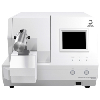
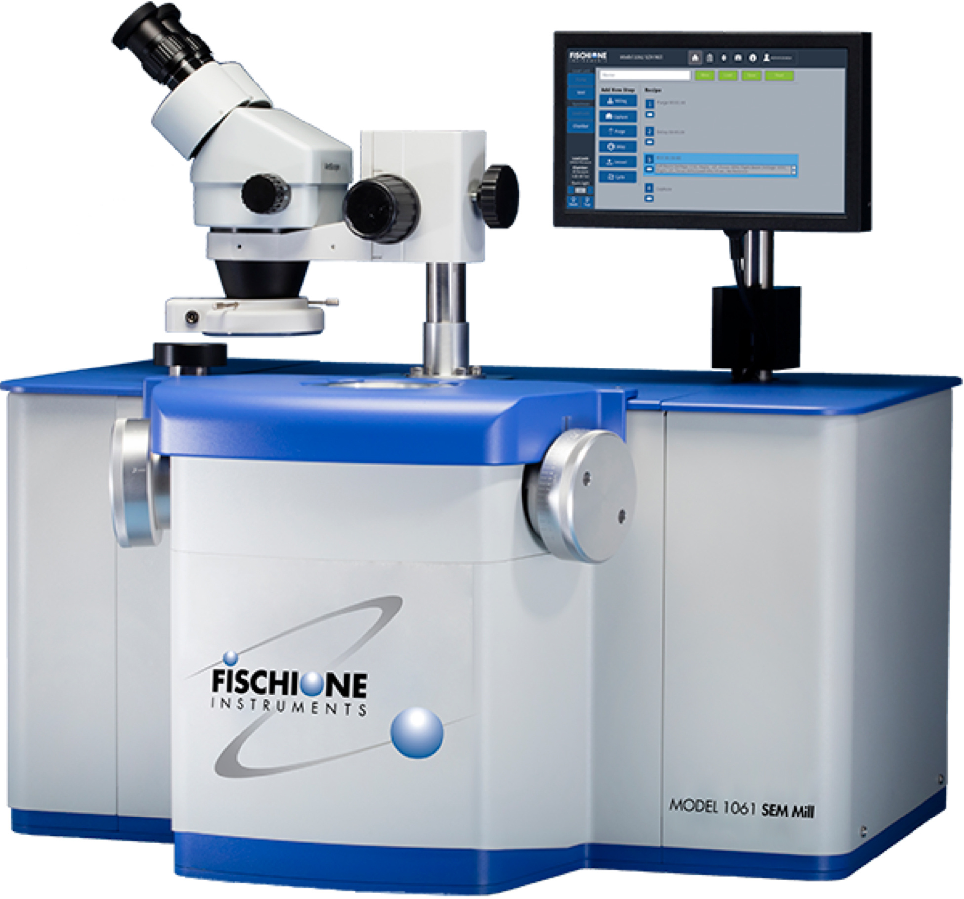
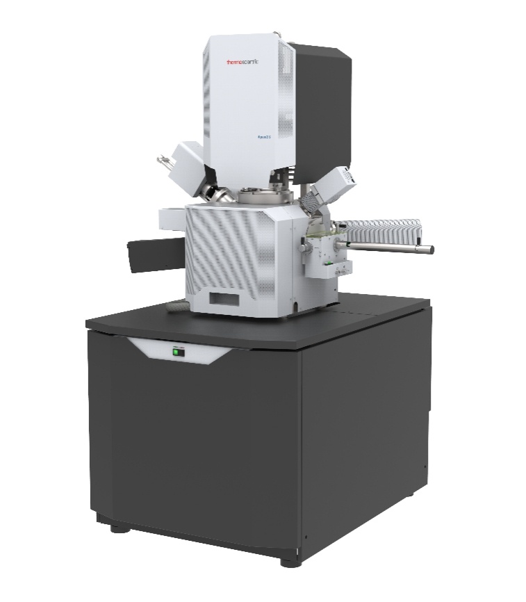
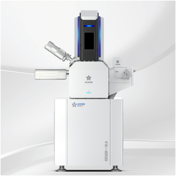
日本电子株式会社(JEOL)为您提供《锂电池材料中表面形貌、化学分析等检测方案(核磁共振)》,该方案主要用于锂电池中表面形貌、化学分析等检测,参考标准--,《锂电池材料中表面形貌、化学分析等检测方案(核磁共振)》用到的仪器有日本电子 JEOL 氩离子截面抛光仪 IB-19530CP、日本电子 JEOL 冷场发射球差校正透射电镜 JEM-ARM200F NEO ARM、日本电子 JSM-IT810场发射扫描电子显微镜、日本电子 JEOL 软X射线分光谱仪 SXES
推荐专场

透射电子显微镜(透射电镜、TEM)
更多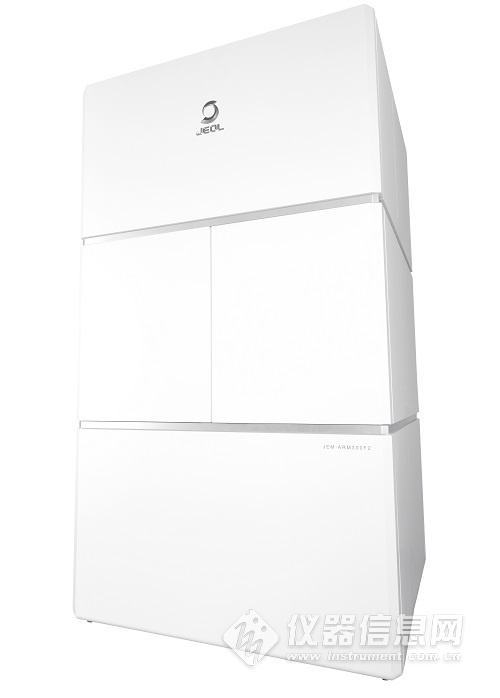

相关方案
更多