
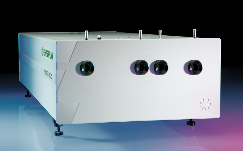


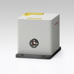
采用立陶宛Ekspla公司纳秒激光泵浦光学参量振荡器NT342A-10,输出激光10Hz, 波长860nm,结合1台150W连续氙灯研究了近红外光电探测器瞬态光伏弛豫性能。
方案详情

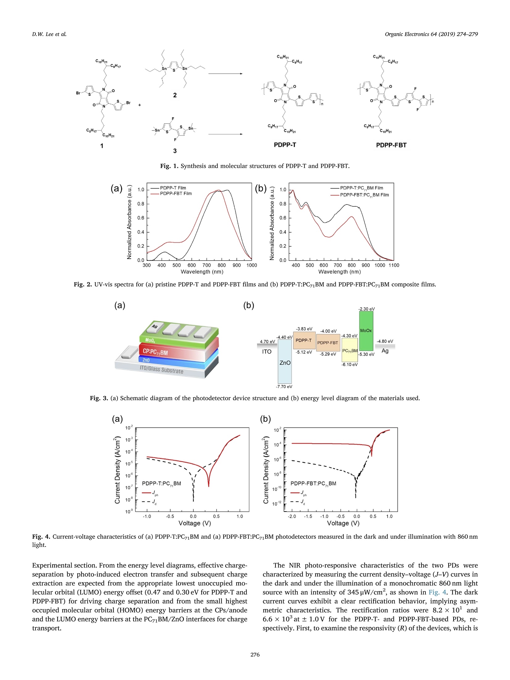
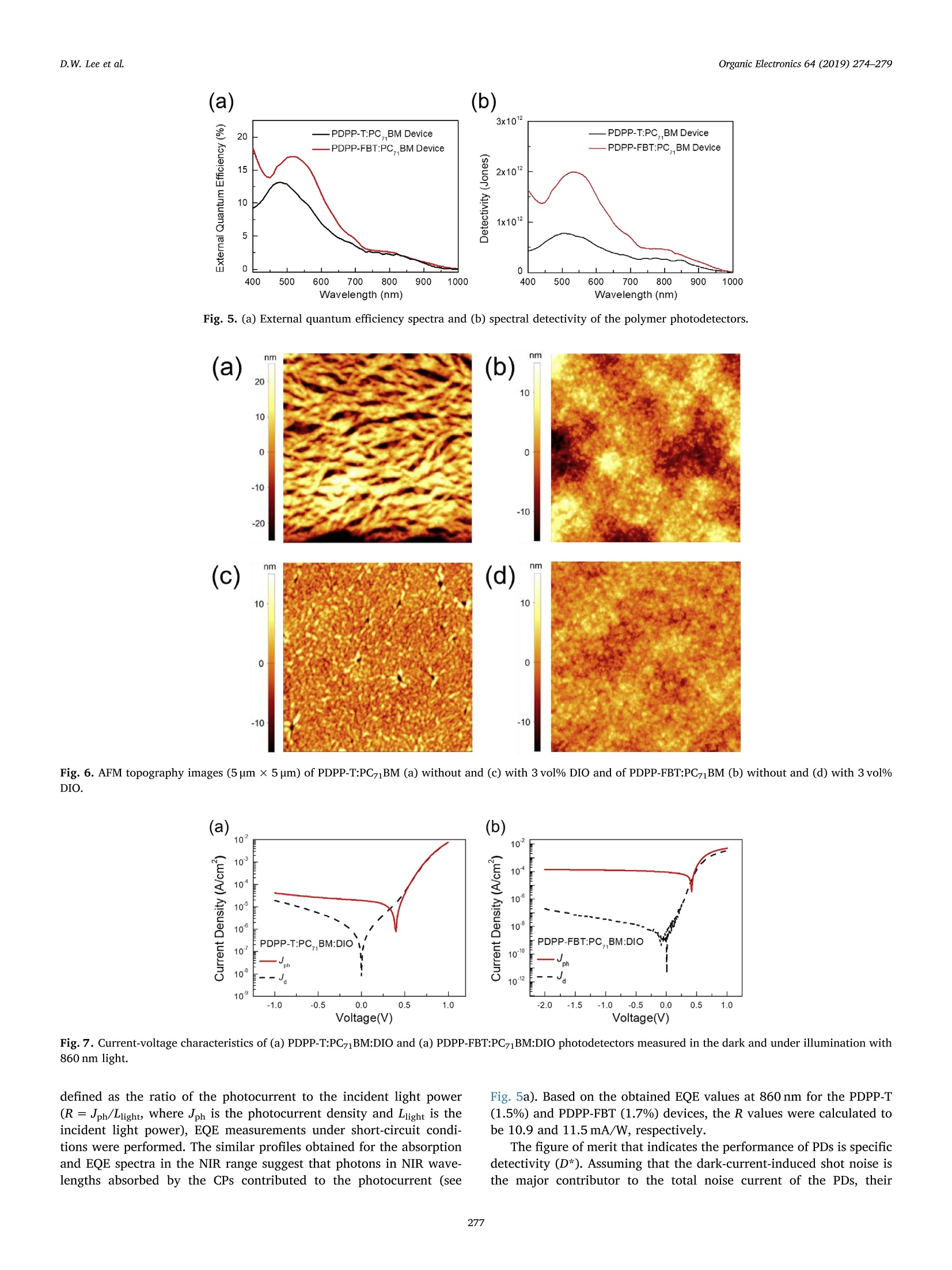
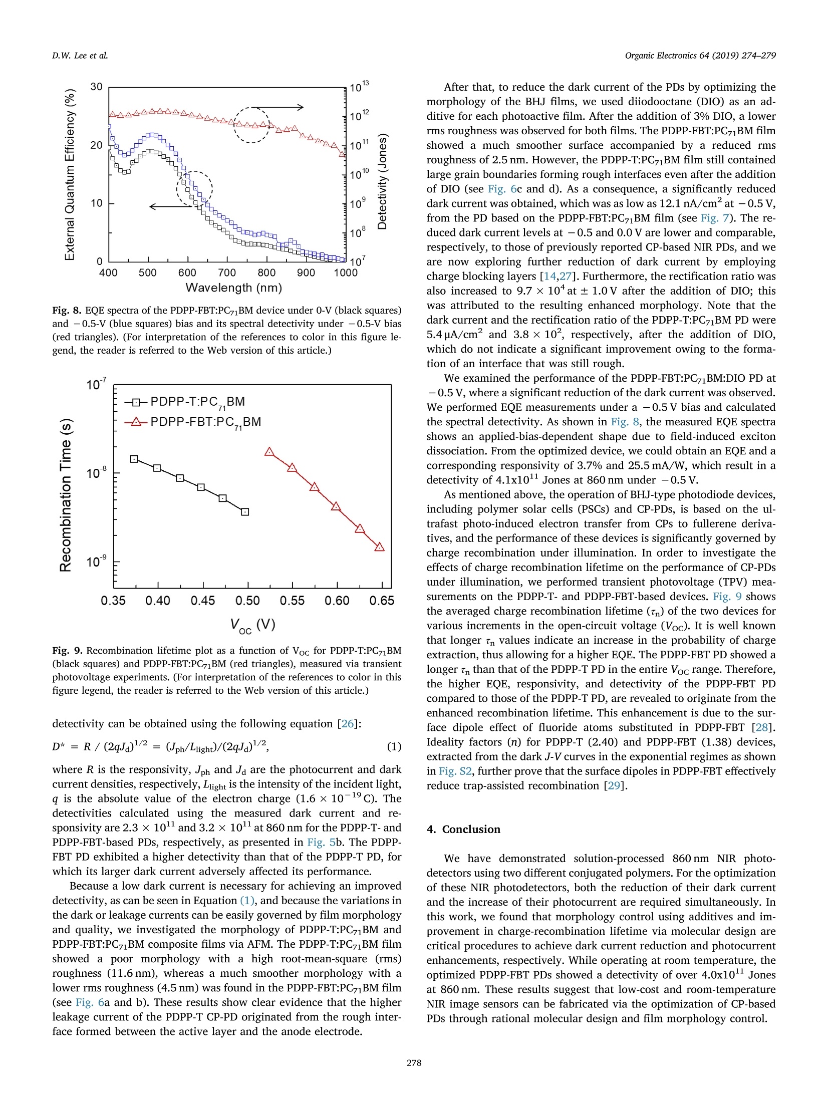
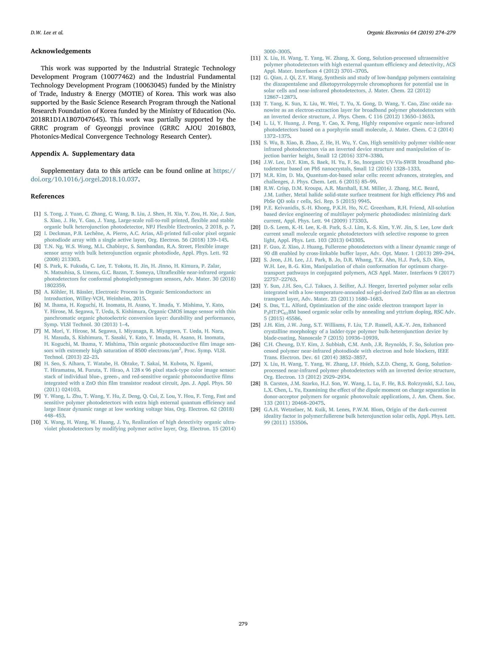
Organic Electronics 64 (2019) 274-279Contents lists available at ScienceDirectOrganic Electronics D.W. Lee et al.Organic Electronics 64 (2019) 274-279 journal homepage: www.elsevier.com/locate/orgel Morphology and charge recombination effects on the performance of near-infrared photodetectors based on conjugated polymers Dae Woon Lee, Yeongkwon Kang, Bong Hyun Jo, Gyeong G. Jeon, Jaehong Park, Sang Eun Yoon , Jian Zheng , Tae Kyu Ahn, Hui Joon Park, Bong-Gi KimD,**, Jong H. Kim,* Department of Molecular Science and Technology, Ajou University, Suwon, 16499, Republic of Korea Division of Chemical Engineering, Konkuk University, Seoul, 05029, Republic of Korea Department of Energy Science, Sungkyunkwan University, Suwon, 16419, Republic of Korea “Department of Energy Systems Research, Ajou University, Suwon, 16499, Republic of Korea ARTICLEINFO ABSTRAC T Keywords:Near-infrared photodetectorConjugated polymersBulk heterojunctionMorphologyCharge recombinationDark current Near-infrared (NIR) photodetectors sensitive to 860 nm light were fabricated through a solution process usingtwo different conjugated polymers (CPs) that share a similar conjugated backbone consisting of a diketo-pyrrolopyrrole (DPP) moiety. The two CPs had a comparable conjugated nature, but their detection capabilitieswere significantly different depending on the applied linker units, namely thiophene for PDPP-Tand fluorinatedthiophene for PDPP-FBT. First, we revealed that employing an additive during active film preparation wasbeneficial for achieving an optimum film morphology for both CPs, which could suppress dark current andprovide enhanced detectivity. In addition, when a highly electronegative fluorine atom, which induces a surfacedipole, was introduced into the conjugated skeleton, it was clearly demonstrated via transient photovoltagemeasurements that the charge recombination time was lengthened, which implies an increase in the probabilityof charge extraction in actual devices by suppressing charge recombination. Thus, PDPP-FBT exhibited higherexternal quantum efficiency and responsivity across all wavelengths. Our results indicated that the managementof both film morphology and surface dipoles of CPs are equally important for achieving high detectivity andresponsivity in organic NIR photodetectors. 1. Introduction Organic photodetectors (OPDs) have attracted considerable atten-tion owing to their applicability in the fabrication of low-cost imagesensors, particularly for applications where flexible or stretchablesubstrates are required [1-4]. The -conjugated organic photosensitivematerials used for OPDs feature much higher absorption coefficients(a > 10 cm-) in the visible range compared to those of inorganicones (asilicon <10cm), the former of which have been used to boostthe photo-detectivity of OPDs [5]. Furthermore, OPDs can effectivelydetect a variety of colors at room temperature by employing absorbersof the corresponding wavelengths without color filters, which is in starkcontrast to conventional silicon (Si)-based photodetectors (PDs), whichrequire the use of color filters for full-color recognition. Because of allthese advantages, image sensors using OPDs integrated with com-plementary metal-oxide semiconductor (CMOS) arrays have already been reported, which has demonstrated the feasibility of full-color or-ganic image sensors [6-8]. Among the various types of OPDs fabricated, since the discovery ofphoto-induced exciton dissociation at bulk heterojunctions (BHJs),OPDs using conjugated-polymer (CP) light absorbers have been in-tensively investigated because of their simplicity in device fabricationand their high charge-separation efficiency [9-11]. Significant researchefforts in CP syntheses and device engineering have allowed for therealization of highly sensitive ultraviolet (UV) and visible-light (Vis)photodetectors. However, only a few near-infrared (NIR) sensitive CPshave been developed so far. For example, Qian et al. and Yang et al.reported NIR photodetectors with detectivities over 101° and 101Jones (1 Jones = 1 cm Hz-/2/W), respectively, by using a low-bandgapNIR absorbing CPs [12,13]. Particularly, OPDs that show reasonable responsivity at wave-lengths longer than 850 nm, which is the critical range for optical ( *Corresponding author. ) ( ** Corresponding a uthor. ) ( E-mail addresses : b g k im201 5 @ ko nku k .a c .kr ( B .-G. K im), j o n g h k i m @aj o u.a c .kr ( J .H.Kim). ) ( T hese authors equally contributed to this work. ) ( ht t p s :// doi.or g/ 1 0 . 1016/j.org e l.2018.10.037 ) ( 1566-11 9 9/C 2018 Elsevier B.V. All rights reserved. ) communications, environmental monitoring, and remote control, arerarely reported owing to the weak absorbance at these wavelengths,charge carrier recombination, high dark current, and difficulties inenergy level alignment [14]. Although an InGaAs NIR photodetector for900-1700 nm detection with a detectivity of over ~1012 Jones hasbeen successfully commercialized, its practical use is still minimal andnot widespread because the device requires cooling to a low tempera-ture (4.2 K) for operation and its fabrication cost is too high because ofits complicated production process [15]. NIR photodetectors based oncolloida quantum dots (QDs) also have attracted considerable attentionbecause of their unique properties including size-tunable spectral sen-sitivity [16]. However, heavy metal such as lead (Pb) is harmful toenvironment and multiple film-coating process is very complicated,which have limited their commercial applications [17,18]. In this context, the low-cost fabrication of NIR-sensitive photo-detectors for longer wavelengths that can operate at room temperatureis highly desirable, and this is expected to be achievable by employingOPDs based on NIR-sensitive CPs. The optimization of dark and photo currents is one of the mostcritical processes for achieving high-detectivity NIR OPDs. So far, mostprevious studies have been focused on the reduction of dark current andincreasing the photo current by inserting hole/electron blocking ortransporting layers [19-21]. However, the original causes that de-termine the intensity of the dark and photo current levels at the pho-toactive layer, rather than at the interfaces, are still unclear. In thiswork, we investigate the effects of the morphology of the photoactivelayers on the dark current and the corresponding detectivity by char-acterizing two different CPs-based NIR OPDs. Furthermore, the corre-lation between the CPs'molecular structure and charge recombinationand their effects on the photo current level and the external quantumefficiency (EQE) of the OPDs in the 860 nm NIR region are explored. 2. Experimental 2.1. Materials All the starting materials used for polymer synthesis were purchasedfrom commercial suppliers (Aldrich and Lumtec) and compound 1 wasprepared following the previously reported method [22]. 6,6-phenyl-C71 butyric acid methyl ester (PC71BM) and diiodooctane (DIO) werepurchased from 1-Material and Sigma-Aldrich,respectively, and used asreceived. The obtained compounds were fully characterized via nuclearmagnetic resonance (NMR) and high-resolution mass spectrometry(HR-MS), and the molecular weight of the final two polymers wascharacterized via gel permeation chromatography (GPC). 2.1.1. PDPP-T Polymerization was carried out in a Schlenk flask under an Ar at-mosphere. Compound 1 (1g, 0.906mmol) and compound 2 (0.6 g,0.906 mmol) were dissolved in anhydrous toluene (15 mL). AfteraddingPd2(dba)3 (0.018g,0.02 mmol)) andP(o-toyl)3 (0.01 g,0.0326 mmol) to the reaction mixture, the solution was stirred vigor-ously at 110℃ for 24 h. Then, 5 mol% of 2-tributylstannyl thiopheneand 2-bromthiophene were added to the reaction mixture in 6h inter-vals, for both the termination of the polymerization process and chain-end modifications. The final polymer was collected via a precipitationtechnique using methanol as a solvent, and the solid was filteredthrough a 0.45-um nylon-membrane filter. The collected solid wasfurther purified via the Soxhlet method using methanol, acetone,hexane, and chloroform. The material soluble only to chloroform wasreprecipitated to obtain the final polymer (Mn: 29,400 and PDI: 2.57). 2.1.2. PDPP-FBT PDPP-FBT (Mn: 32,200 and PDI: 2.24) was synthesized in the sameway as PDPP-T but using compound 1 (0.42 g, 0.382 mmol) and com-pound 3 (0.18 g, 0.382 mmol). OPDs were fabricated on indium tin oxide (ITO)-coated glass sub-strates. The substrates were cleaned via sonication in detergent/deio-nized water, acetone, and isopropyl alcohol for 15 min each. Then, thesubstrates were dried in a nitrogen (N2) stream and further cleaned viaan UV-ozone treatment for 10 min. Zinc oxide (ZnO) layers were pre-pared on top of the cleaned ITO/glass substrates following a previouslyreported sol-gel spin-coating and annealing process [23]. The NIRphotosensitive layer was prepared by spin-coating with a blend solutionof the two conjugated polymers (PDPP-T and PDPP-FBT) and PC71BM(1:2, w/w) with a concentration of 18 mg/mL in chloroform/di-chlorobenzene on the ZnO layer in a N2-filled glove box. Then, a 10 nm-thick molybdenum oxide (MoOx) layer was deposited via vacuumthermal evaporation under 3.0 × 10⁻⁶Torr with an evaporation rate of0.2A/s. The fabrication of the devices was completed with the de-position of 100 nm-thick silver (Ag) electrode via vacuum thermalevaporation under 3.0x10⁻⁶Torr with an evaporation rate of 1.0 A/s. Ashadow mask was used to make the active device area be 5.0 mm. 2.3. Characterization The current density-voltage (J-V) measurements of the devices wereperformed using a Keithley 4200 semiconductor characterizationsystem under a simulated AM 1.5G spectrum with a power of 100 mW/cm²(1 sun), generated using a solar simulator (Newport, LCS-100,94011A). The EQE spectra were obtained using an incident-photon-to-current conversion efficiency (IPCE) setup consisting of a xenon lamp(Newport, 450W) and a monochromator. The light intensity at eachwavelength was calibrated with a standard single-crystal silicon pho-tovoltaic cell. The UV-Vis absorption spectra of the CP:PC71BM filmswere measured using a UV-vis spectrophotometer (Jasco V-770).Measurements on the morphology of the films were performed viaatomic force microscopy (AFM, Park System PE-100) in tapping mode.Transient photovoltage decay measurements were performed using ananosecond laser-pumped (pulsed at 10 Hz, NT342A-10,EKSPLA) op-tical parametric oscillator with 860 nm pulses and a xenon lamp (con-tinuous wave, 150 W, Zolix); these devices were used as an attenuatedperturbation-light pulse source and a bias light source, respectively.The devices were electrically connected to a digital oscilloscope(500 MHz, DSO-X 3054A, Agilent) with BNC cables, and the input im-pedance was set to be 1 MQ (Keithley 2001) to create open-circuitconditions. The bias light intensity was controlled using neutral densityfilters (from 0.0 to 1.0 sun) to generate various open circuit voltages.For the photocurrent measurements of the devices, a termination withan input impedance of 50 Ω was used instead to create closed-circuitconditions without making any changes to the optical setup. 3. Results and discussion The molecular structures of the two CPs used in this study (PDPP-Tand PDPP-FBT) are shown in Fig. 1. Both CPs were synthesized via Stillecoupling reactions, as described in the Experimental section. Fig. 2presents the UV-vis absorption spectra of pristine PDPP-T and PDPP-FBT thin-films and those of PDPP-T:PC71BM and PDPP-FBT:PC71BMcomposite films. The new absorption bands between 300 and 500 nm inthe composite films originate from the absorption of PC71BM, and nosubstantial changes in the spectra of the two CPs were observed afterthe addition of PC71BM to the CPs. The neat PDPP-T and PDPP-FBTfilms showed absorption onsets at 960 and 955 nm, which correspondto optical band-gaps (E,s) of 1.29 and 1.30 eV. The device structure of the photodetector (ITO/ZnO/CP:PC71BM/MoOx/Ag) and the energy level diagrams of the materials used areshown in Fig. 3 [24,25]. Energy levels were determined based on ul-traviolet photoelectron spectroscopy (UPS) measurements and Eg’s (seeFig. S1). The device fabrication method is described in detail in the Fig. 1. Synthesis and molecular structures of PDPP-T and PDPP-FBT. Fig. 2. UV-vis spectra for (a) pristine PDPP-T and PDPP-FBT films and (b) PDPP-T:PC71BM and PDPP-FBT:PC71BM composite films. (a) (b) Fig. 3. (a) Schematic diagram of the photodetector device structure and (b) energy level diagram of the materials used. Fig. 4. Current-voltage characteristics of (a) PDPP-T:PC71BM and (a) PDPP-FBT:PC71BM photodetectors measured in the dark and under illumination with 860 nmlight. Experimental section. From the energy level diagrams, effective charge-separation by photo-induced electron transfer and subsequent chargeextraction are expected from the appropriate lowest unoccupied mo-lecular orbital (LUMO) energy offset (0.47 and 0.30 eV for PDPP-T andPDPP-FBT) for driving charge separation and from the small highestoccupied molecular orbital (HOMO) energy barriers at the CPs/anodeand the LUMO energy barriers at the PC71BM/ZnO interfaces for chargetransport. The NIR photo-responsive characteristics of the two PDs werecharacterized by measuring the current density-voltage (J-V) curves inthe dark and under the illumination of a monochromatic 860 nm lightsource with an intensity of 345 uW/cm, as shown in Fig. 4. The darkcurrent curves exhibit a clear rectification behavior, implying asym-metric characteristics. The rectification ratios were 8.2 × 10 and6.6 × 10at ±1.0V for the PDPP-T- and PDPP-FBT-based PDs, re-spectively. First, to examine the responsivity (R) of the devices,which is defined as the ratio of the photocurrent to the incident light power(R=Jph/Llight where Jph is the photocurrent density and Llight is theincident light power), EQE measurements under short-circuit condi-tions were performed. The similar profiles obtained for the absorptionand EQE spectra in the NIR range suggest that photons in NIR wave-lengths absorbed by the CPs contributed to the photocurrent (see (a) (b) 一20 ——PDPP-T:PC,BM DevicecwcEw -PDPP-FBT:PC_BM Device 15 10 5 0 400 500 600 700 800 900 1000 Wavelength (nm) Fig.5. (a) External quantum efficiency spectra and (b) spectral detectivity of the polymer photodetectors. Fig. 6. AFM topography images (5 um ×5 um) of PDPP-T:PC71BM (a) without and (c) with 3 vol% DIO and of PDPP-FBT:PC71BM (b) without and (d) with 3 vol%DIO. Fig.7. Current-voltage characteristics of (a) PDPP-T:PC71BM:DIO and (a) PDPP-FBT:PC71BM:DIO photodetectors measured in the dark and under illumination with860 nm light. Fig. 5a). Based on the obtained EQE values at 860 nm for the PDPP-T(1.5%) and PDPP-FBT (1.7%) devices, the R values were calculated tobe 10.9 and 11.5 mA/W, respectively. The figure of merit that indicates the performance of PDs is specificdetectivity (D*). Assuming that the dark-current-induced shot noise isthe major contributor to the total noise current of the PDs, their Fig.8. EQE spectra of the PDPP-FBT:PC71BM device under 0-V (black squares)and -0.5-V(blue squares) bias and its spectral detectivity under -0.5-V bias(red triangles). (For interpretation of the references to color in this figure le-gend, the reader is referred to the Web version of this article.) V(V) Fig. 9. Recombination lifetime plot as a function of Voc for PDPP-T:PC71BM(black squares) and PDPP-FBT:PC71BM (red triangles), measured via transientphotovoltage experiments. (For interpretation of the references to color in thisfigure legend, the reader is referred to the Web version of this article.) where R is the responsivity, Jph and Ja are the photocurrent and darkcurrent densities, respectively,Llight is the intensity of the incident light,q is the absolute value of the electron charge (1.6×10⁻¹⁹ C). Thedetectivities calculated using the measured dark current and re-sponsivity are 2.3 ×10and 3.2×10at 860 nm for the PDPP-T- andPDPP-FBT-based PDs, respectively, as presented in Fig. 5b. The PDPP-FBT PD exhibited a higher detectivity than that of the PDPP-T PD, forwhich its larger dark current adversely affected its performance. Because a low dark current is necessary for achieving an improveddetectivity, as can be seen in Equation (1), and because the variations inthe dark or leakage currents can be easily governed by film morphologyand quality, we investigated the morphology of PDPP-T:PC71BM andPDPP-FBT:PC71BM composite films via AFM. The PDPP-T:PC71BM filmshowed a poor morphology with a high root-mean-square (rms)roughness (11.6 nm), whereas a much smoother morphology with alower rms roughness (4.5 nm) was found in the PDPP-FBT:PC71BM film(see Fig. 6a and b). These results show clear evidence that the higherleakage current of the PDPP-T CP-PD originated from the rough inter-face formed between the active layer and the anode electrode. After that, to reduce the dark current of the PDs by optimizing themorphology of the BHJ films, we used diiodooctane (DIO) as an ad-ditive for each photoactive film. After the addition of 3% DIO, a lowerrms roughness was observed for both films. The PDPP-FBT:PC71BM filmshowed a much smoother surface accompanied by a reduced rmsroughness of 2.5 nm. However, the PDPP-T:PC71BM film still containedlarge grain boundaries forming rough interfaces even after the additionof DIO (see Fig. 6c and d). As a consequence, a significantly reduceddark current was obtained, which was as low as 12.1 nA/cm’at -0.5V,from the PD based on the PDPP-FBT:PC71BM film (see Fig. 7). The re-duced dark current levels at -0.5 and 0.0 V are lower and comparable,respectively, to those of previously reported CP-based NIR PDs, and weare now exploring further reduction of dark current by employingcharge blocking layers [14,27]. Furthermore, the rectification ratio wasalso increased to 9.7 x 10at ±1.0V after the addition of DIO; thiswas attributed to the resulting enhanced morphology. Note that thedark current and the rectification ratio of the PDPP-T:PC71BM PD were5.4uA/cm’ and 3.8x10², respectively, after the addition of DIO,which do not indicate a significant improvement owing to the forma-tion of an interface that was still rough. We examined the performance of the PDPP-FBT:PC71BM:DIO PD at-0.5 V, where a significant reduction of the dark current was observed.We performed EQE measurements under a -0.5V bias and calculatedthe spectral detectivity. As shown in Fig. 8, the measured EQE spectrashows an applied-bias-dependent shape due to field-induced excitondissociation. From the optimized device, we could obtain an EQE and acorresponding responsivity of 3.7% and 25.5 mA/W, which result in adetectivity of 4.1x10 Jones at 860 nm under -0.5 V. As mentioned above, the operation of BHJ-typephotodiode devices,including polymer solar cells (PSCs) and CP-PDs, is based on the ul-trafast photo-induced electron transfer from CPs to fullerene deriva-tives, and the performance of these devices is significantly governed bycharge recombination under illumination. In order to investigate theeffects of charge recombination lifetime on the performance of CP-PDsunder illumination, we performed transient photovoltage (TPV) mea-surements on the PDPP-T-and PDPP-FBT-based devices. Fig. 9 showsthe averaged charge recombination lifetime (tn) of the two devices forvarious increments in the open-circuit voltage (Voc). It is well knownthat longer tn values indicate an increase in the probability of chargeextraction, thus allowing for a higher EQE. The PDPP-FBT PD showed alonger tn than that of the PDPP-T PD in the entire Voc range. Therefore,the higher EQE, responsivity, and detectivity of the PDPP-FBT PDcompared to those of the PDPP-T PD, are revealed to originate from theenhanced recombination lifetime. This enhancement is due to the sur-face dipole effect of fluoride atoms substituted in PDPP-FBT [28].Ideality factors (n) for PDPP-T(2.40) and PDPP-FBT (1.38) devices,extracted from the dark J-V curves in the exponential regimes as shownin Fig. S2, further prove that the surface dipoles in PDPP-FBT effectivelyreduce trap-assisted recombination [29]. 4. Conclusion We have demonstrated solution-processed 860nm NIR photo-detectors using two different conjugated polymers. For the optimizationof these NIR photodetectors, both the reduction of their dark currentand the increase of their photocurrent are required simultaneously. Inthis work, we found that morphology control using additives and im-provement in charge-recombination lifetime via molecular design arecritical procedures to achieve dark current reduction and photocurrentenhancements, respectively. While operating at room temperature, theoptimized PDPP-FBT PDs showed a detectivity of over 4.0x10 Jonesat 860 nm. These results suggest that low-cost and room-temperatureNIR image sensors can be fabricated via the optimization of CP-basedPDs through rational molecular design and film morphology control. Acknowledgements This work was supported by the Industrial Strategic TechnologyDevelopment Program (10077462) and the Industrial FundamentalTechnology Development Program (10063045) funded by the Ministryof Trade, Industry & Energy (MOTIE) of Korea. This work was alsosupported by the Basic Science Research Program through the NationalResearch Foundation of Korea funded by the Ministry of Education (No.2018R1D1A1B07047645). This work was partially supported by theGRRC program of Gyeonggiiprovince (GRRC AJOUJ2016B03.Photonics-Medical Convergence Technology Research Center). Appendix A. Supplementary data Supplementary data to this article can be found online at https://doi.org/10.1016/j.orgel.2018.10.037. ( References ) ( [ 1] S . T on g , J. Y u a n, C . Z ha ng, C . Wa ng , B . L iu, J. S h en, H. Xi a , Y . Z o u , H. Xi e , J . S un , S . X iao, J . H e , Y . Ga o , J . Ya ng , L arg e -scale ro l l-to- r oll p r inted, f l ex i bl e a nd st a ble o rga n i c b u l k h ete r o ju nct i on pho t odet e c t or , N P J F l ex i bl e E lec tr o n i cs , 2 2 0 1 8 , p. 7. ) ( [2] I . D eckm a n, P .B. Le c hene, A. Pi e r r e , A. C . Ar i a s, A l l - p rin t ed full - col o r pix e l or g a nic p hotodiode a r ray w i t h a s i ngle a ctiv e l a y e r , O r g . E le ctro n. 5 6 ( 20 18) 1 3 9 - 14 5 . ) ( [ 3] T . N . N g , W .S . W ong, M .L . C h a b i n y c , S . S a m b a ndan, R. A . S t r e e t , F l e x i b le i m a g e s 18 . en sor a rray w it h b ul k h et e r oj u n ct i o n or g a ni c ph o t od i o de , A p p l . Ph y s yS. . Le t t . 9 2 (2008) 21 3 303. ) ( [4] S . Pa r k, K. F u kuda , C . L e e , T. Y okota, H. J i n , H . J i nno , H . K i mura , P . Z al a r , N . M a t su h i sa , S . U m ez u , G . C. Baz a n, T . So m e ya , U l tr a f l ex i b l e n ea r - i n f rar e d o r ga n i c p ho t ode te ctors f or c onfo rm a l p h ot op let h ys m og r a m s enso r s, Adv . Ma t e r. 30 ( 201 8 ) 1802359. ) ( [5] A . K ohler , H . B as s l er , E l ect ronic P ro c es s i n O rg an i c Sem i c ondu ct o r s: an I ntr o du c t ion , Will e y - V C H, W einh e i m, 2015. ) ( [6] M . I h a ma , H . K o g u ch i, H. I n oma t a, H . A sa no, Y. I m a da , Y. M i sh i ma, Y. K a t o , Y . H i ro se, M. S eg aw a , T . Ue d a , S. K i shim u r a , O r ga nic CM O S imag e se ns o r w i t h t h i n p a n ch r omatic o r g an i c ph ot oele c t r i c co n version l ay er : du r abilit y a n d perf o rmance, S ymp. V L S I T e c hnol. 3 0 ( 2013) 1 -4 . ) ( [7 ] M . M o ri, Y . H irose, M . S eg a wa , I . M i ya n a g a , R . M iy a g a wa , T . U e d a , H . Na r a, H . M a su d a, S . K i s h imur a , T . S as a k i, Y . K a to , Y . I m a d a, H . As ano, H . I n o ma t a, H . K o gu c hi , M . Ih ama , Y . M i s h ima, Th i n org a ni c p h o tocondu c t i ve fi lm imag e se n - s o r s w i t h e x tremely h i g h sa t u rat i on o f 8 5 00 ele c tro n s/ u m , P r o c . Sy m p . VL S I . T e c h no l . ( 201 3 ) 2 2 - 23 . ) ( [8] H . Se o, S . A ihara , T . Wa t ab e , H . O htake , T. Sa kai , M. K u bota, N . E g am i , T . H i r am at s u , M . F u r u t a, T . H i r a o, A 1 2 8 x 9 6 pi x e l sta c k-t y p e c ol o r i m a g e s e n so r: stac k o f i ndi v i d u a l b lue - , g reen- , a nd r ed -sens itive o rga n ic p h oto co ndu c ti v e fi l ms i nte gr a t e d w i t h a Z nO thi n f il m tra n s i s t or rea d o u t c i rc u i t, Jpn . J . Ap p l . P h y s . 5 0 ( 2 01 1 ) 0241 03 . ) ( [9] Y . W an g , L . Z h u , T. W a ng , Y. H u , Z . D e n g, Q. C u i, Z . L ou , Y . H ou , F . T e ng , Fas t a n d s e n s itiv e p o ly m er p h otodetectors w i th e x tra h i g h e x ter n al q u a ntum e fficie nc y an d l arg e lin ear dy na m i c r a n ge at l o w w o rk i n g vol t ag e bi as , O r g . El e c t r on . 6 2 ( 2 0 18 ) 448-453. ) ( [10] X . W ang , H . W a ng , W . H u a ng, J. Y u , Re ali z ation of hi g h de tecti v it y o r g an ic u l tra- v i o le t photodete c tor s b y modifying p oly m e r ac t i ve l aye r , Org. E l e c tron. 15 (201 4 ) ) ( 3 000 - 3 005. ) ( [ 11] X . L iu , H . W ang , T . Ya ng, W . Z h a n g, X. G o n g , So l utio n - p roc es se d u l t r a se nsi ti v e p o l yme r p h o todete c to r s w it h h i g h e x t ernal q u a nt um ef f ic i ency and dete cti v it y, AC S A ppl . M a t er. I nterfa c es 4 ( 201 2 ) 3701 -3 705. ) ( [12] G . Q ia n , J . Qi, Z.Y . W a n g, Syn t h es is a n d stu d y o f l o w -ban dg a p polym er s cont a i n i ng t he d i a zapen t a l en e an d diketo p yr r ol op y r role c h r o m op h o r es fo r po t entia l u s e i n s o l a r c el l s and near- i nfrare d p h otodetec t or s , J. M ater. Ch em. 2 2 (2 0 12)1286 7- 1287 3 . ) ( [13 ] T . Y a n g, K . S un , X . L i u , W. W ei, T . Y u , X . G o n g , D. W a n g, Y . C a o , Z i n c o x id e n a - n owire a s an e lectr o n -e x t ra c ti o n l ay e r f or broadband po l ym e r ph o t ode t ector s wit h a n i nverte d de vi c e s t r u c tu r e, J. Ph ys . Chem . C 1 1 6 ( 201 2) 1 3 65 0 - 1 3 6 53. ) ( [14] L i . L i, Y. Huang, J . Pe n g, Y. C a o , X . Pe n g, Highly r es po n siv e o r ganic n e a r - i nfr a red p h o t o d e t e c t ors b as e d on a p o r p h yr i n s m a l l m o le cul e, J . M at e r . C hem. C 2 (2 014 ) 1 372- 1 3 75. ) ( [15] S . W u, B . X i a o, B . Z h ao , Z . He , H. Wu , Y . C ao, Hi g h se ns i t i vit y p o l y me r vi s i b le- n e a r i n fr ar e d p h otodet e c t ors v i a a n i n ver t e d d ev i ce s tructur e a n d manipul at i on of i n - j e ct ion b a rr ier hei g h t , Sm a l l 1 2 ( 20 1 6 ) 3 37 4- 338 0. ) ( [ 16] J .W. L ee , D . Y . K im, S . B a ek , H . Y u, F . S o , I n o r g a n ic UV- V is - SWIR b r oa d b a n d p h o - todetec t or based on P b S n an o crys t als , Small 12 ( 2016) 1 328- 13 33. ) [17]M.R. Kim, D. Ma, Quantum-dot-based solar cells: recent advances, strategies, andchallenges, J. Phys. Chem. Lett.6 (2015) 85-99. ( [18] R . W. C r i sp, D . M . K r o up a , A . R . M a r shal l ,E.M . Mi l l er , J . Z h a ng , M . C. B e a rd , J . M . L ut h er, M et al h a li d e s o lid - s t at e su r f ac e t r eat m ent f o r h igh ef f i cie nc y PbS and P b Se Q D so l a r c e l ls , Sc i . R ep. 5 ( 2 015 ) 9 945. ) [19] P.E. Keivanidis, S.-H. Khong, P.K.H. Ho, N.C. Greenham, R.H. Friend, All-solutionbased device engineering of multilayer polymeric photodiodes: minimizing darkcurrent, Appl. Phys. Lett. 94 (2009) 173303. ( [20] D I . - S . L eem, K . -H . L e e, K .- B . P a r k, S . -J. L im, K .- S. K i m , Y . W. J in, S. Lee , Low d a r k c urre n t s mall m olec ul e or g a n ic p h otod e te c to r s wi th s e le ct ive r esponse t o g r een l i ght , A ppl. P hy s. L ett . 10 3 ( 201 3 ) 04 33 0 5 . ) [21] F. Guo, Z. Xiao, J. Huang, Fullerene photodetectors with a linear dynamic range of90 dB enabled by cross-linkable buffer layer, Adv. Opt. Mater.1 (2013) 289-294. [22] S. Jeon, J.H. Lee, J.I. Park, B. Jo, D.R. Whang, T.K. Ahn, H.J. Park, S.D. Kim, W.H. Lee, B.-G. Kim, Manipulation of chain conformation for optimum charge-transport pathways in conjugated polymers, ACS Appl. Mater. Interfaces 9 (2017)22757-22763. [23]Y. Sun, J.H. Seo, C.J. Takacs, J. Seifter, A.J. Heeger, Inverted polymer solar cellsintegrated with a low-temperature-annealed sol-gel-derived ZnO film as an electrontransport layer, Adv. Mater. 23 (2011)1680-1683. [24] S. Das, T.L. Alford, Optimization of the zinc oxide electron transport layer inPsHT:PC61BM based organic solar cells by annealing and yttrium doping, RSC Adv.5 (2015) 45586. ( [ 25] J . H. K i m , J .W . Ju ng , S. T. W i l li a m s , F . L iu , T . P . R u s sell, A . K . - Y . J en , E nh a n ce d r . c r yst a l l i ne morpho log y o f a l adder- typ e poly me r b u lk - h et e ro j u nc t i o n devi ce by b l ade - coat in g , N anosc a l e 7 (20 15 ) 1 0936 - 10939. ) [26]C.H. Cheung, D.Y. Kim, J. Subbiah, C.M. Amb, J.R.Reynolds, F. So, Solution pro-cessed polymer near-infrared photodiode with electron and hole blockers, IEEETrans. Electron. Dev. 61 (2014) 3852-3857. ( [ 2 7] X . L iu, H. Wa n g , T. Y a n g, W . Zha ng , I . F . H s i e h , S .Z . D. Che ng , X. Gon g , Soluti o n- p rocess e d n ear- i nfrared poly m e r p hoto d etectors w it h a n inve rt e d dev i c e s tructure, O r g . El e ctro n. 1 3 (20 1 2)2929 -2 934. ) ( [28]B I . C a r s t e n , J .M . S zark o, H . J. S o n, W . W a ng, L . L u , F . H e , B .S . R o l cz y ns k i , S . J . L o u , L .X . C h en, L . Y u , E xa m i nin g t he e f f ect of th e di po l e mome n t o n cha r g e s epa r at i on in d onor- a ccept o r po ly m ers fo r o rga n ic ph otovo l taic appl i c a t ions, J. Am. Chem. So c. 1 33 ( 2 0 1 1) 20 4 68-20 4 75. ) ( [29] G . A . H.W e tzel a er, M . K u i k, M . L e ne s , P.W .M. Bl o m, O ri g i n of t h e da r k - cu rr ent i deali t y f actor in polymer: f u l le r e n e b ulk het e r o junction s o lar cells, Appl. P hys . L e tt. 9 9( 2 011) 15 3506. ) Received September Received in revised form October Accepted October vailable online October Near-infrared (NIR) photodetectors sensitive to 860 nm light were fabricated through a solution process using two different conjugated polymers (CPs) that share a similar conjugated backbone consisting of a diketopyrrolopyrrole (DPP) moiety. The two CPs had a comparable conjugated nature, but their detection capabilities were significantly different depending on the applied linker units, namely thiophene for PDPP-T and fluorinatedthiophene for PDPP-FBT. First, we revealed that employing an additive during active film preparation was beneficial for achieving an optimum film morphology for both CPs, which could suppress dark current and provide enhanced detectivity. In addition, when a highly electronegative fluorine atom, which induces a surface dipole, was introduced into the conjugated skeleton, it was clearly demonstrated via transient photovoltage measurements that the charge recombination time was lengthened, which implies an increase in the probability of charge extraction in actual devices by suppressing charge recombination. Thus, PDPP-FBT exhibited higher external quantum efficiency and responsivity across all wavelengths. Our results indicated that the management of both film morphology and surface dipoles of CPs are equally important for achieving high detectivity and responsivity in organic NIR photodetectors.
确定
还剩4页未读,是否继续阅读?

产品配置单
北京欧兰科技发展有限公司为您提供《近红外光电探测器中瞬态光伏弛豫检测方案(激光产品)》,该方案主要用于电子元器件产品中瞬态光伏弛豫检测,参考标准--,《近红外光电探测器中瞬态光伏弛豫检测方案(激光产品)》用到的仪器有Ekspla NT340 高能量可调谐激光器(OPO)
推荐专场

相关方案
更多
该厂商其他方案
更多