


方案详情
文
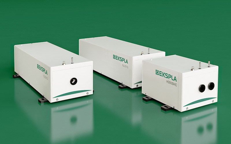
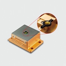
采用立陶宛Ekspla公司的NL303G型激光器的基频1064nm,10Hz输出重复频率,利用分光技术分成两束,然后在一个2X2平方毫米的区域内形成强度周期性变化的干涉条纹,并利用这一光束进行不定形硅的结晶化处理。
方案详情

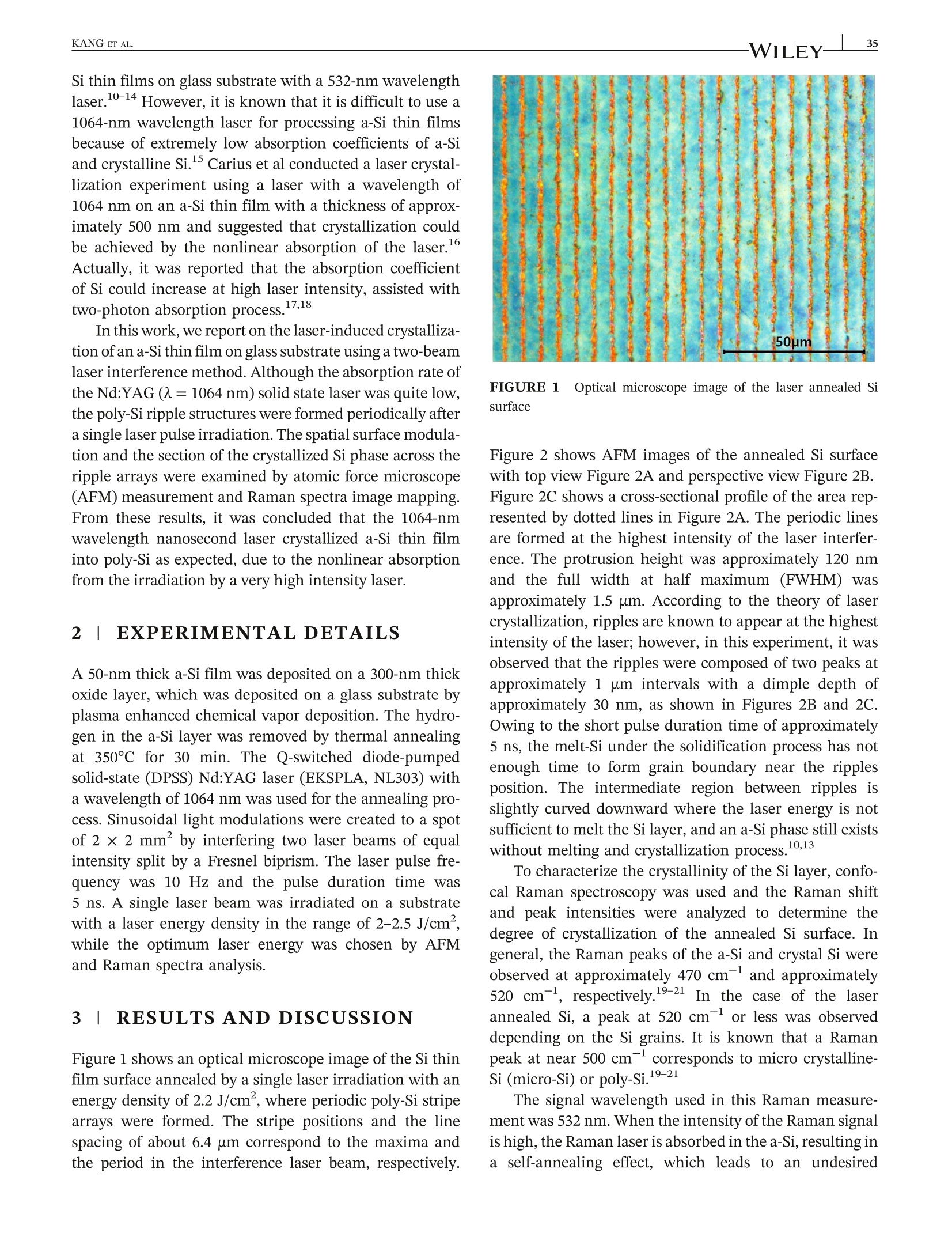
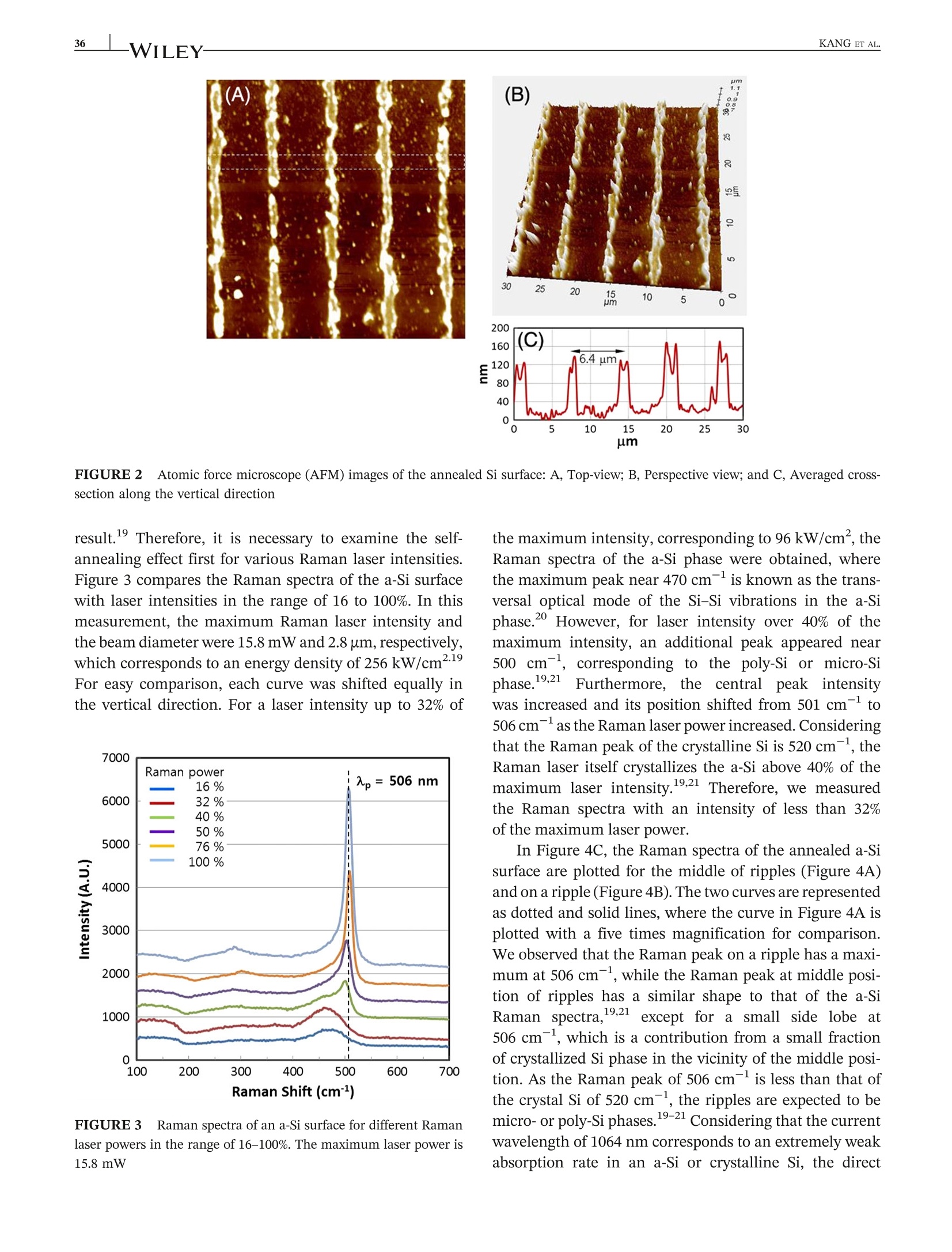
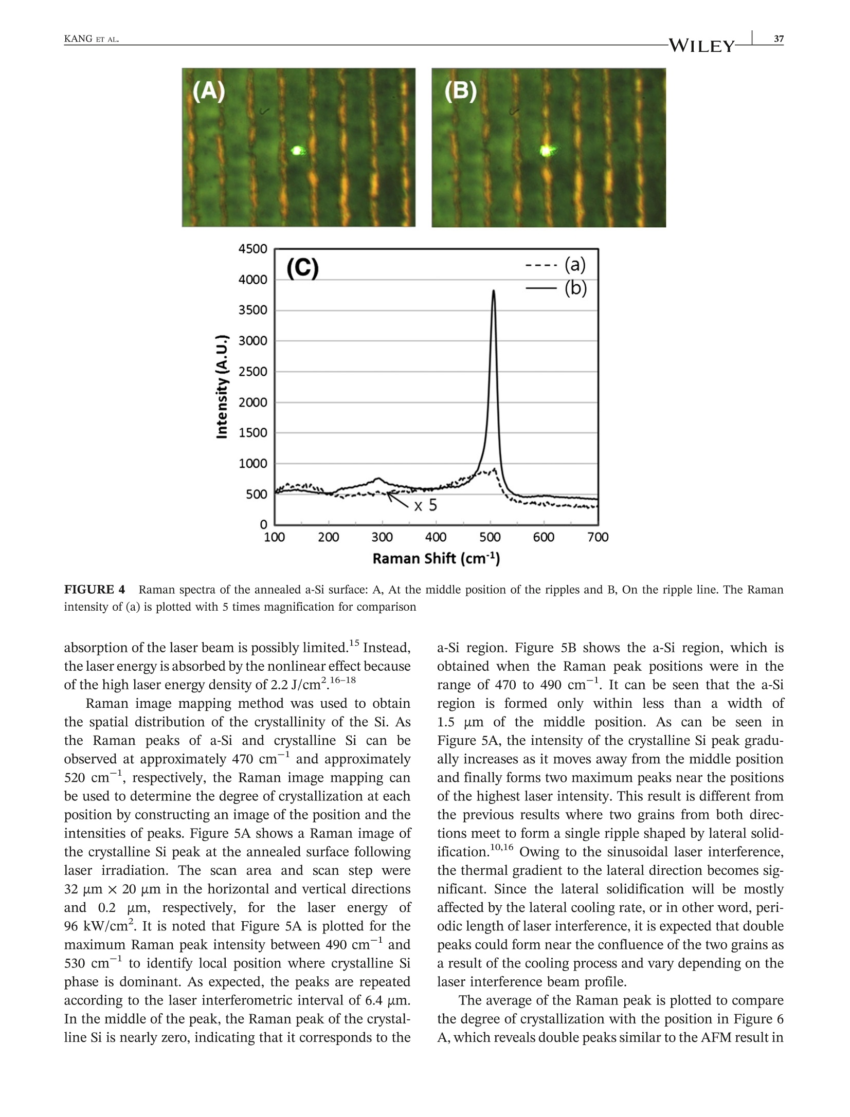
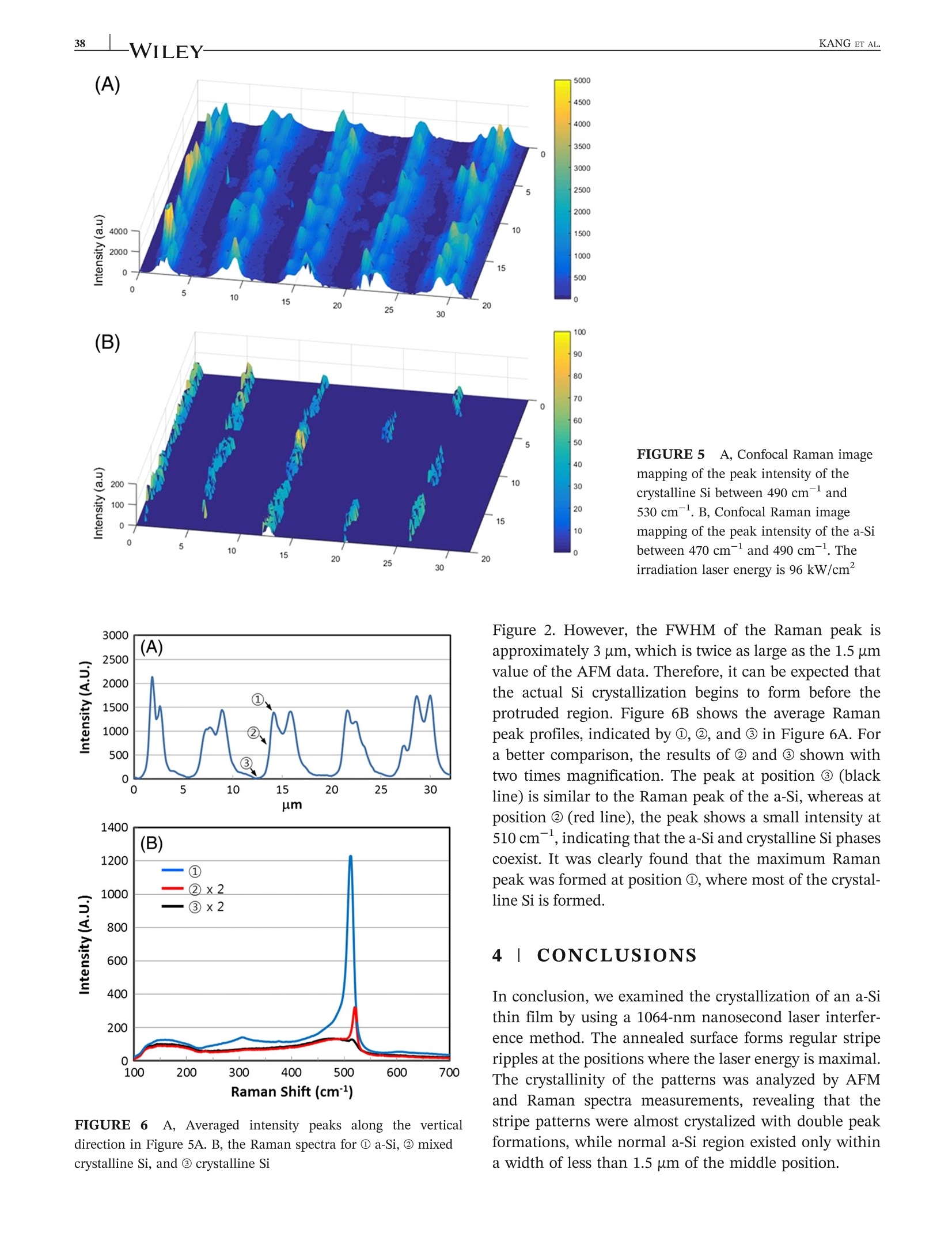
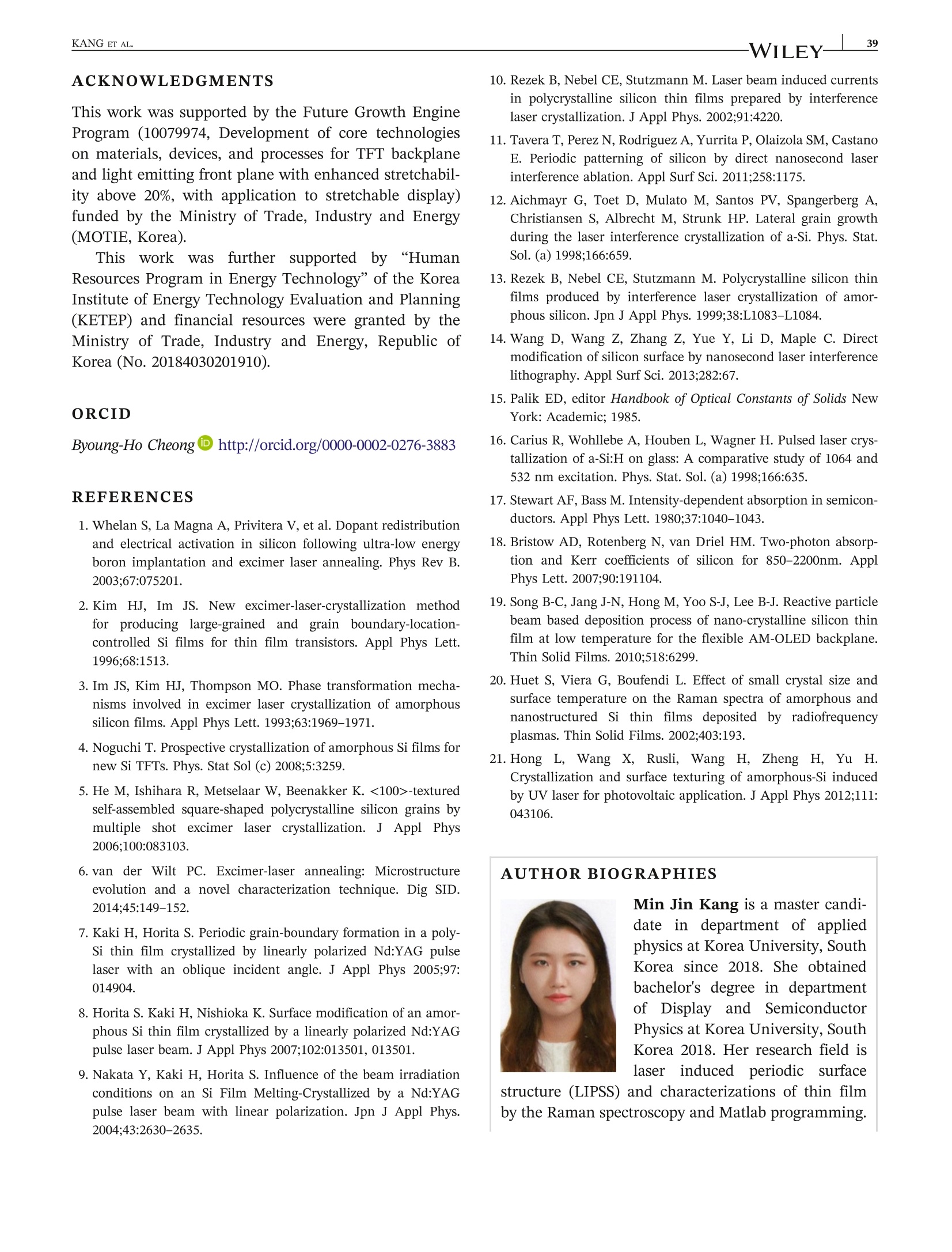
Revised: 3 October 2018Accepted: 20 October 2018Received: 15 August 2018DOI: 10.1002/jsid.745WILEY 35KANG ET AL.-WILEY-, 34wileyonlinelibrary.com/journal/jsidJ Soc Inf Display. 2018;27:34-40. REGULARCONTRIBUTEDPAPE R Crystallization of amorphous-Si using nanosecond laserinterference method Min Jin Kang1 Minyeong KimI Eui Sun Hwang1 Jiwhan Noh’1 Sung Tae Shin1Byoung-Ho CheongiD Department of Applied Physics, KoreaUniversity, Sejong, Republic of KoreaDepartment of Laser Application, KoreaInstitute of Machinery & Materials(KIMM), Daejeon, Republic of Korea Correspondence Byoung-Ho Cheong and Sung Tae Shin,Department of Applied Physics, KoreaUniversity 2511 Sejong-ro, Sejong, 30019Republic of Korea.Email: bhcheong84@korea.ac.kr; stshin@korea.ac.kr Funding information Ministry of Trade, Industry and Energy,Republic of Korea, Grant/Award Number:20184030201910; Future Growth EngineProgram, Grant/Award Number:10079974 Abstract Laser crystallization of a 50-nm thick amorphous-Si (a-Si) thin film on glasssubstrate was examined by a Nd:YAG (A= 1064 nm) nanosecond laser and atwo-beam laser interference method. In spite of the low absorption rate ofthe laser wavelength in the a-Si, crystallized Si ripple patterns were observedfollowing a single laser pulse irradiation. The atomic force microscope (AFM)measurement revealed that surface ripple arrays are protruded as high as120 nm at the positions corresponding to the maximum laser intensity andthe ripples are composed of narrow double peaks with a separation of1 um.Raman image mapping was used to plot the spatial distribution of the crystal-lized Si phase. It was found that a 1064-nm-wavelength nanosecond laser couldcrystallize an a-Si thin film into polycrystalline-Si (poly-Si) by nonlinearabsorption under high laser energy irradiation. KEYWORDS recrystallization, semiconducting silicon, single crystal growth, surface structure 11]INTRODUCTION Laser annealing, including the activation of ultra-shallowjunction in semiconductor devices or low-temperaturepolysilicon (LTPS) process in display or solar cell devicesis a widely used technique in Si-based devices.1-3 TheLTPS process is a well-established method to obtainpolycrystalline-Si (poly-Si) grains from amorphous-Si(a-Si).3-6Currently, the LTPS process is performedusing a 308-nm wavelength XeCl excimer laser, convertingthe a-Si to uniform poly-Si grains of approximately300 nm.Solid-state lasers of 355 nm or 532 nm wave-lengths have also been explored as alternatives to excimerlasers, owing to their quite stable operation and achievable output, which is as high as that of excimer lasers.How-ever, since the LTPS method involves quite complicatedprocesses like light absorption, heat transfer, solid-to-liquid phase changes, and cooling process within tens ofnanoseconds, it is difficult to form uniform and well-ordered poly-Si grains in a large area.2-9 Compared with a laser annealing process that irradi-ates a laser to a substrate at a uniform intensity, onefeature of the laser interference process is that the laserintensity is periodically modulated; thus, periodic surfacetextures can be formed conveniently.-TThere havebeen several reports on laser interference processes, suchas periodic patterning on Si wafers with lasers of 355 nmand 1064 nm wavelengths and poly-Si crystallization of a- ( @ 2018 The Authors. Journal of the S o ciety for I nformation Display published by W i ley Periodicals, Inc. o n behalf o f Society for Information D isplay ) ( This i s an open a ccess a rticle under the terms o f the Creative Commons Attribution-NonCommercial Licens e ,which permits use, dis t ribution and rep r oduction in any medium, pr o vided the original wo r k is properly cit e d and is n ot use d for commercial purposes. ) Si thin films on glass substrate with a 532-nm wavelengthlaser.10-14 However, it is known that it is difficult to use a1064-nm wavelength laser for processing a-Si thin filmsbecause of extremely low absorption coefficients of a-Siand crystalline Si.5 Carius et al conducted a laser crystal-lization experiment using a laser with a wavelength of1064 nm on an a-Si thin film with a thickness of approx-imately 500 nm and suggested that crystallization couldbe achieved by the nonlinear absorption of the laser.Actually, it was reported that the absorption coefficientof Si could increase at high laser intensity, assisted withtwo-photon absorption process.17,18 In this work, we report on the laser-induced crystalliza-tion of an a-Si thin film on glass substrate using a two-beamlaser interference method. Although the absorption rate ofthe Nd:YAG (1=1064 nm) solid state laser was quite low,the poly-Si ripple structures were formed periodically aftera single laser pulse irradiation. The spatial surface modula-tion and the section of the crystallized Si phase across theripple arrays were examined by atomic force microscope(AFM) measurement and Raman spectra image mapping.From these results, it was concluded that the 1064-nmwavelength nanosecond laser crystallized a-Si thin filminto poly-Si as expected, due to the nonlinear absorptionfrom the irradiation by a very high intensity laser. 2 EXPERIMENTAL DETAILS A 50-nm thick a-Si film was deposited on a 300-nm thickoxide layer, which was deposited on a glass substrate byplasma enhanced chemical vapor deposition. The hydro-gen in the a-Si layer was removed by thermal annealinga1at350℃ for 30 min. The Q-switched diode-pumpedsolid-state (DPSS) Nd:YAG laser (EKSPLA,NL303) witha wavelength of 1064 nm was used for the annealing pro-cess. Sinusoidal light modulations were created to a spotof 2 × 2 mm by interfering two laser beams of equalintensity split by a Fresnel biprism. The laser pulse fre-quency was 10 Hz and the pulse duration time was5 ns. A single laser beam was irradiated on a substratewith a laser energy density in the range of 2-2.5 J/cm ,while the optimum laser energy was chosen by AFMand Raman spectra analysis. 3 RESULTSAND DISCUSSION Figure 1 shows an optical microscope image of the Si thinfilm surface annealed by a single laser irradiation with anenergy density of 2.2 J/cm’, where periodic poly-Si stripearrays were formed. The stripe positions and the linespacing of about 6.4 um correspond to the maxima andthe period in the interference laser beam, respectively. FIGURE 1COptical microscope image of the laser annealed Sisurface Figure 2 shows AFM images of the annealed Si surfacewith top view Figure 2A and perspective view Figure 2B.Figure 2C shows a cross-sectional profile of the area rep-resented by dotted lines in Figure 2A. The periodic linesare formed at the highest intensity of the laser interfer-ence. The protrusion height was approximately 120 nmand the full width at half maximum (FWHM) wasapproximately 1.5 um. According to the theory of lasercrystallization, ripples are known to appear at the highestintensity of the laser; however, in this experiment, it wasobserved that the ripples were composed of two peaks atapproximately 1 um intervals with a dimple depth ofapproximately 30 nm, as shown in Figures 2B and 2C.Owing to the short pulse duration time of approximately5 ns, the melt-Si under the solidification process has notenough time to form grain boundary near the ripplesposition. The intermediate region between ripples isslightly curved downward where the laser energy is notsufficient to melt the Si layer, and an a-Si phase still existswithout melting and crystallization process.10,13 To characterize the crystallinity of the Si layer, confo-cal Raman spectroscopy was used and the Raman shiftand peak intensities were analyzed to determine thedegree of crystallization of the annealed Si surface. Ingeneral, the Raman peaks of the a-Si and crystal Si wereobserved at approximately 470 cm-and approximately520 cm-, respectively.19-211In the case of the laserannealed Si, a peak at 520 cm- or less was observeddepending on the Si grains. It is known that a Ramanpeak at near 500 cm- corresponds to micro crystalline-Si (micro-Si) or poly-Si.9-21 The signal wavelength used in this Raman measure-ment was 532 nm. When the intensity of the Raman signalis high, the Raman laser is absorbed in the a-Si, resulting ina self-annealing effect, which leads to an undesired FIGURE 2 Atomic force microscope (AFM) images of the annealed Si surface: A, Top-view; B, Perspective view; and C, Averaged cross-section along the vertical direction result. Therefore, it is necessary to examine the self-annealing effect first for various Raman laser intensities.Figure 3 compares the Raman spectra of the a-Si surfacewith laser intensities in the range of 16 to 100%. In thismeasurement, the maximum Raman laser intensity andthe beam diameter were 15.8 mW and 2.8 um, respectively,which corresponds to an energy density of 256 kW/cm219For easy comparison, each curve was shifted equally inthe vertical direction. For a laser intensity up to 32% of FIGURE 3 Raman spectra of an a-Si surface for different Ramanlaser powers in the range of 16-100%.The maximum laser power is15.8 mW the maximum intensity, corresponding to 96 kW/cm, theRaman spectra of the a-Si phase were obtained, wherethe maximum peak near 470 cm-is known as the trans-versal optical mode of the Si-Si vibrations in the a-Siphase.20 However, for laser intensity over 40% of themaximum intensity, an additional peak appeared near500 cm, corresponding to the poly-Si or micro-Siphase.19,21Furthermore, the central peakintensitywas increased and its position shifted from 501 cm-to506 cm-as the Raman laser power increased. Consideringthat the Raman peak of the crystalline Si is 520 cm, theRaman laser itself crystallizes the a-Si above 40% of themaximum laser intensity.19,21 Therefore, we measuredthe Raman spectra with an intensity of less than 32%of the maximum laser power. In Figure 4C, the Raman spectra of the annealed a-Sisurface are plotted for the middle of ripples (Figure 4A)and on a ripple (Figure 4B). The two curves are representedas dotted and solid lines, where the curve in Figure 4A isplotted with a five times magnification for comparison.We observed that the Raman peak on a ripple has a maxi-mum at 506 cm,while the Raman peak at middle posi-tion of ripples has a similar shape to that of the a-SiRaman spectra,19.21except for a small side lobe at506 cm,which is a contribution from a small fractionof crystallized Si phase in the vicinity of the middle posi-tion. As the Raman peak of 506 cm-is less than that ofthe crystal Si of 520 cm-, the ripples are expected to bemicro-or poly-Si phases.19-21 Considering that the currentwavelength of 1064 nm corresponds to an extremely weakabsorption rate in an a-Si or crystalline Si, the direct (A) (B) Raman Shift (cm") FIGURE 4 Raman spectra of the annealed a-Si surface: A, At the middle position of the ripples and B, On the ripple line. The Ramanintensity of (a) is plotted with 5 times magnification for comparison absorption of the laser beam is possibly limited.Instead,the laser energy is absorbed by the nonlinear effect becauseof the high laser energy density of 2.2 J/cm2.16-18 Raman image mapping method was used to obtainthe spatial distribution of the crystallinity of the Si. Asthe Raman peaks of a-Si and crystalline Si can beobserved at approximately 470 cm-and approximately520 cm, respectively, the Raman image mapping canbe used to determine the degree of crystallization at eachposition by constructing an image of the position and theintensities of peaks. Figure 5A shows a Raman image ofthe crystalline Si peak at the annealed surface followinglaser irradiation. The scan area and scan step were32 um × 20 um in the horizontal and vertical directionsand0.2 um, respectively, for the laser energy of96 kW/cm. It is noted that Figure 5A is plotted for themaximum Raman peak intensity between 490 cm-and530 cm- to identify local position where crystalline Siphase is dominant. As expected, the peaks are repeatedaccording to the laser interferometric interval of 6.4 um.In the middle of the peak, the Raman peak of the crystal-line Si is nearly zero, indicating that it corresponds to the a-Si region. Figure 5B shows the a-Si region, which isobtained when the Raman peak positions were in therange of 470 to 490 cm. It can be seen that the a-Siregion is formed only within less tthan awidth of1.55 um of the middle position. As can be seen inFigure 5A, the intensity of the crystalline Si peak gradu-ally increases as it moves away from the middle positionand finally forms two maximum peaks near the positionsof the highest laser intensity. This result is different fromthe previous results where two grains from both direc-tions meet to form a single ripple shaped by lateral solid-ification.10,16 Owing to the sinusoidal laser interference,the thermal gradient to the lateral direction becomes sig-nificant. Since the lateral solidification will be mostlyaffected by the lateral cooling rate, or in other word, peri-odic length of laser interference, it is expected that doublepeaks could form near the confluence of the two grains asa result of the cooling process and vary depending on thelaser interference beam profile. The average of the Raman peak is plotted to comparethe degree of crystallization with the position in Figure 6A, which reveals double peaks similar to the AFM result in 5000 100 90 80 70 60 50 40 30 20 10 0 FIGURE 6 A, Averaged intensity peaks along the verticaldirection in Figure 5A. B, the Raman spectra for ① a-Si, ② mixedcrystalline Si, and ③ crystalline Si Figure 2. However, the FWHM of the Raman peak isapproximately 3 um, which is twice as large as the 1.5 umvalue of the AFM data. Therefore, it can be expected thatthe actual Si crystallization begins to form before theprotruded region. Figure 6B shows the average Ramanpeak profiles, indicated by ①, ②, and ③ in Figure 6A. Fora better comparison, the results of② and ③ shown withtwo times magnification. The peak at position ③ (blackline) is similar to the Raman peak of the a-Si, whereas atposition ② (red line), the peak shows a small intensity at510 cm, indicating that the a-Si and crystalline Si phasescoexist. It was clearly found that the maximum Ramanpeak was formed at position ①, where most of the crystal-line Si is formed. 4. CONCLUSIONS In conclusion, we examined the crystallization of an a-Sithin film by using a 1064-nm nanosecond laser interfer-ence method. The annealed surface forms regular striperipples at the positions where the laser energy is maximal.The crystallinity of the patterns was analyzed by AFMand Raman spectra measurements, revealing that thestripe patterns were almost crystalized with double peakformations, while normal a-Si region existed only withina width of less than 1.5 um of the middle position. This work was supported by the Future Growth EngineProgram (10079974, Development of core technologieson materials, devices, and processes for TFT backplaneand light emitting front plane with enhanced stretchabil-ity above 20%, with application to stretchable display)funded by the Ministry of Trade, Industry and Energy(MOTIE, Korea). This work wasfurther supported tby“HumanResources Program in Energy Technology”of the KoreaInstitute of Energy Technology Evaluation and Planning(KETEP) and financial resources were granted by theMinistry of Trade, Industry and Energy, Republic ofKorea (No. 20184030201910) ORCID Byoung-Ho Cheong http://orcid.org/0000-0002-0276-3883 REFERENCES ( 1. Whelan S, La M a gna A, P ri v itera V, e t al. Do p ant redistribution and electrical a ctivation i n s ilicon f ollowing ultra-low e n ergyboron i mplantation and e xcimer l aser annealing. Phys Rev B. 2003;67:075201. ) ( 2. Kim H J, Im J S . New exc i mer-laser-crystallization method for producing l arge-grained andgrain b oundary-location-controlled S i f ilms for thin f i lm tr a nsistors. A p pl Phys Lett . 1996;68:1513. ) ( 3. Im JS, Kim HJ, Thompson MO. P h ase t r ansformation mecha- nisms involved in excimer l a ser crystallization of amorphoussilicon films. Appl P hys L e tt. 1993;63:1969-1971. ) ( 4. Noguchi T. Prospective crystallization of amorphous Si f i lms fornew S i TFTs. P h ys. S t at S o l (c) 2008;5:3259. ) ( 5. He M, Ishihara R, Metselaar W, Beenakker K. <100>-textured self-assembled square-shaped po l ycrystalline silicon gr a ins by multiple shot excimer l a ser c r ystallization. J Appl Phys2006;100:083103. ) ( 6. van der W ilt P C. E x cimer-laser annealing: Microstructureevolution and a novel characterization t echnique. D ig SID. 2014;45:149-152. ) ( 7.Kaki H, H o rita S. P e riodic grain-boundary formation in a poly-Si t hin f ilm c rystallized by l inearly polarized N d:YAG pu l selaser with a n o blique i n cident a n gle. J A p pl Ph y s 200 5 ;97: 014904. ) ( 8. Horita S. Kaki H, Nishioka K. Surface modification of an amor- phous Si thin film c rystallized by a linearly polarized Nd:YAG pulse laser beam. J Appl Phys 2007;102:013501, 0 13501. ) ( 9. Nakata Y , K aki H, H o rita S. I n fluence of the beam irr a diation conditions on an Si Film Melting-Crystallized by a Nd:YAGpulse laser beam w ith l inear p olarization. Jpn J Appl Phys. 2004;43:2630-2635. ) ( 10. Rezek B, Nebel CE, Stutzmann M . Laser beam induced currents in p olycrystalline silicon thin films prepared b y i n terference laser crystallization. J Appl Phys. 2002;91:4220. ) 11. Tavera T,Perez N, Rodriguez A, Yurrita P, Olaizola SM, CastanoE. Periodic patterning of silicon by direct nanosecond laserinterference ablation. Appl Surf Sci. 2011;258:1175. 12. Aichmayr G, Toet D, Mulato M, Santos PV, Spangerberg A,Christiansen S, Albrecht M, Strunk HP. Lateral grain growthduring the laser interference crystallization of a-Si. Phys. Stat.Sol. (a) 1998;166:659. 13. Rezek B, Nebel CE, Stutzmann M. Polycrystalline silicon thinfilms produced by interference laser crystallization of amor-phous silicon. Jpn J Appl Phys. 1999;38:L1083-L1084. 14. Wang D, Wang Z, Zhang Z, Yue Y, Li D, Maple C. Directmodification of silicon surface by nanosecond laser interferencelithography. Appl Surf Sci. 2013;282:67. 15. Palik ED, editor Handbook of Optical Constants of Solids NewYork: Academic; 1985. 16. Carius R, Wohllebe A, Houben L, Wagner H. Pulsed laser crys-tallization of a-Si:H on glass: A comparative study of 1064 and532 nm excitation. Phys. Stat. Sol. (a) 1998;166:635. 17. Stewart AF, Bass M. Intensity-dependent absorption in semicon-ductors. Appl Phys Lett. 1980;37:1040-1043. 18. Bristow AD, Rotenberg N, van Driel HM. Two-photon absorp-tion and Kerr coefficients of silicon for 850-2200nm. ApplPhys Lett. 2007;90:191104. 19. Song B-C, Jang J-N, Hong M, Yoo S-J, Lee B-J. Reactive particlebeam based deposition process of nano-crystalline silicon thinfilm at low temperature for the flexible AM-OLED backplane.. Thin Solid Films. 2010;518:6299. 20. Huet S, Viera G, Boufendi L. Effect of small crystal size andsurface temperature on the Raman spectra of amorphous andnanostructured Sithin films deposited by radiofrequencyplasmas. Thin Solid Films. 2002;403:193. ( 21. Hong LL, Wang X, Rusli 1 . , W ang H , Zheng HI. , Yu H.Crystallization and surface texturing of amorphous-Si i n ducedby UV l a ser for p hotovoltaic a pplication. J Appl Phys 2 012;111: 043106. ) AUTHOR BIOGRAPHIES Min Jin Kang is a master candi-date in department of appliedphysics at Korea University, SouthKorea since 2018. She obtainedbachelor’s degree in departmentof Display andSemiconductorPhysics at Korea University, SouthKorea 2018. Her research field isiaserrinduced periodiccsurface structure (LIPSS) and characterizations of thin filmby the Raman spectroscopy and Matlab programming. Minyeong Kim is an undergrad-uate student in department of Dis-play and Semiconductor Physics atKorea University, South Korea.She is in charge of atomic forcemicroscope measurement andnumerical simulations of photonicdevices using Matlab andCOMSOL package. Eui Sun Hwang is a master can-didate in department of appliedphysics at Korea University, SouthKorea since 2018. He obtainedbachelor’s degree in departmentof Display andd SSemiconductorPhysics at Korea University, SouthKorea 2018. His research field isphotonic device fabrications based on high-k dielectric nano-patterns. Jiwhan Noh, Ph. D., has been aprincipal researcher attKIMM(Korea Institute of Machinery &Materials), South Korea since 2005,conducting research in the fieldof laser-material interaction andlaser optics devices. Before joiningKIMM, Noh was a senior engineera1tSamsung electronics co. He received Ph.D. degree in Mechanical engineering fromKorea Advanced Institute of Science and Technology,South Korea. Sung Tae Shin, Ph. D., is cur-rently a Full Prof. at Korea Univer-sity and Executive Vice President atLight Polymers located in SouthSan Francisco in USA. He had beena Senior Vice President for the LCDBusiness at Samsung Electronicsand Samsung Display Co. was spunoff from Samsung Electronics on April 1, 2012 in Korea since January 1, 2008. As thehead of the Next Generation Display DevelopmentTeam, he was in charge of research and development of future technologies for new displays. He was theDirector of the Display R&D Center from January2009 to April 2010, and also previously worked as aPrincipal Engineer in 1994 to begin the developmentof the Pattern Vertical Alignment (PVA) Mode, whichis currently under Monitor and TV mass production.He joined Department of Display & SemiconductorPhysics at Korea University as Assistant Prof. in 1997,and he had worked as Associate Prof. and Prof. until2007 for ten years. His research fields during that timewere flexible display, 3D display, and a new liquid crys-tal mode concerned fast response time and wide viewangle. Additionally, Dr. Shin is currently President atKorean Information Display Society (KIDS), and hasserved as the Principal Vice President, Vice President,Director of General Secretary, Academic, and Indus-trial Cooperation at KIDS for more than twelve yearssince 2002. He asspresident of KIDS is GeneralChair of IMID 2018. Dr.Shin earned a B.S. in Physicsat Korea University in South Korea and a Ph. D in thefield of liquid crystal in Physics at Kent State Universityin the United States in May 1994. Byoung-Ho Cheong, Ph. D., hasbeen a professor at Korea Univer-sity, South Koreasince:2016.conducting research in the fieldof laser-material interaction andnano-photonic devices. Beforejoining Korea University, Cheongwas a principal engineer atSamsung Display co. and Samsung Advanced Institute of Technology. He received a Master’s and Ph.D. degree in physics from Korea Advanced Institute of Science and Technology, South Korea. He received his bachelor’s degree in physics from Korea University, South Korea. How to cite this article: Kang MJ, Kim M,Hwang ES, Noh J, Shin ST, Cheong B-H.Crystallization of amorphous-Si using nanosecondlaser interference method. J Soc Inf Display.2019;27:34-40. https://doi.org/10.1002/jsid.745 Laser crystallization of a 50‐nm thick amorphous‐Si (a‐Si) thin film on glass substrate was examined by a Nd:YAG (λ = 1064 nm) nanosecond laser and a two‐beam laser interference method. In spite of the low absorption rate of the laser wavelength in the a‐Si, crystallized Si ripple patterns were observed following a single laser pulse irradiation. The atomic force microscope (AFM) measurement revealed that surface ripple arrays are protruded as high as120 nm at the positions corresponding to the maximum laser intensity and the ripples are composed of narrow double peaks with a separation of 1 μm.Raman image mapping was used to plot the spatial distribution of the crystallized Si phase. It was found that a 1064‐nm‐wavelength nanosecond laser could crystallize an a‐Si thin film into polycrystalline‐Si (poly‐Si) by nonlinear absorption under high laser energy irradiation.
确定
还剩5页未读,是否继续阅读?

产品配置单
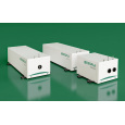
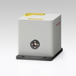
北京欧兰科技发展有限公司为您提供《不定形硅中结晶化检测方案(激光产品)》,该方案主要用于其他中结晶化检测,参考标准--,《不定形硅中结晶化检测方案(激光产品)》用到的仪器有NL300系列高能量电光调Q激光器
推荐专场
相关方案
更多