


方案详情
文
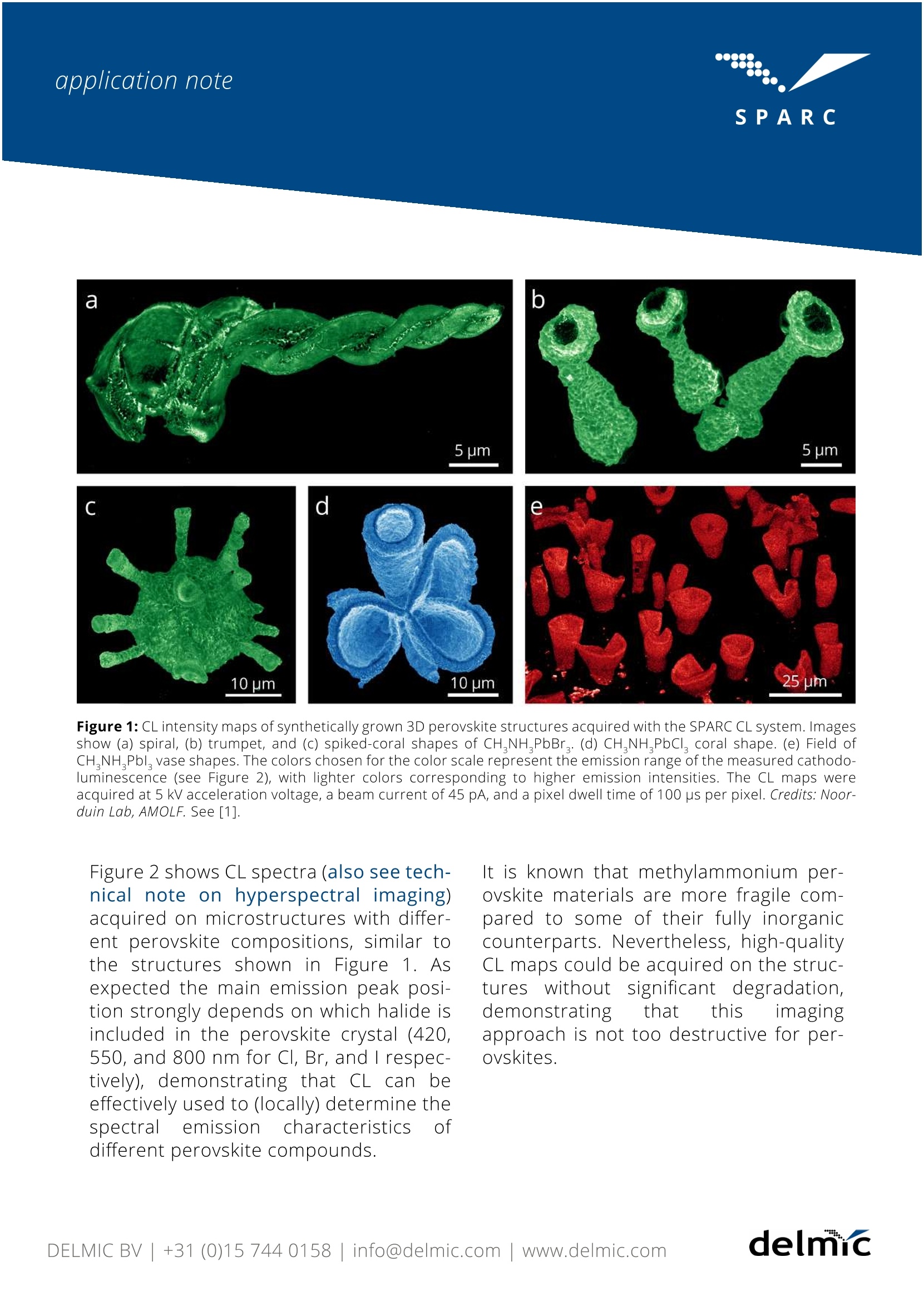
While most of the time perovskites are grown in a more traditional shape of thin-films and nanocrystals, it was discovered recently that with the use of carbonate salts perovskite materials can take a large variety of complex 3D shapes.
方案详情

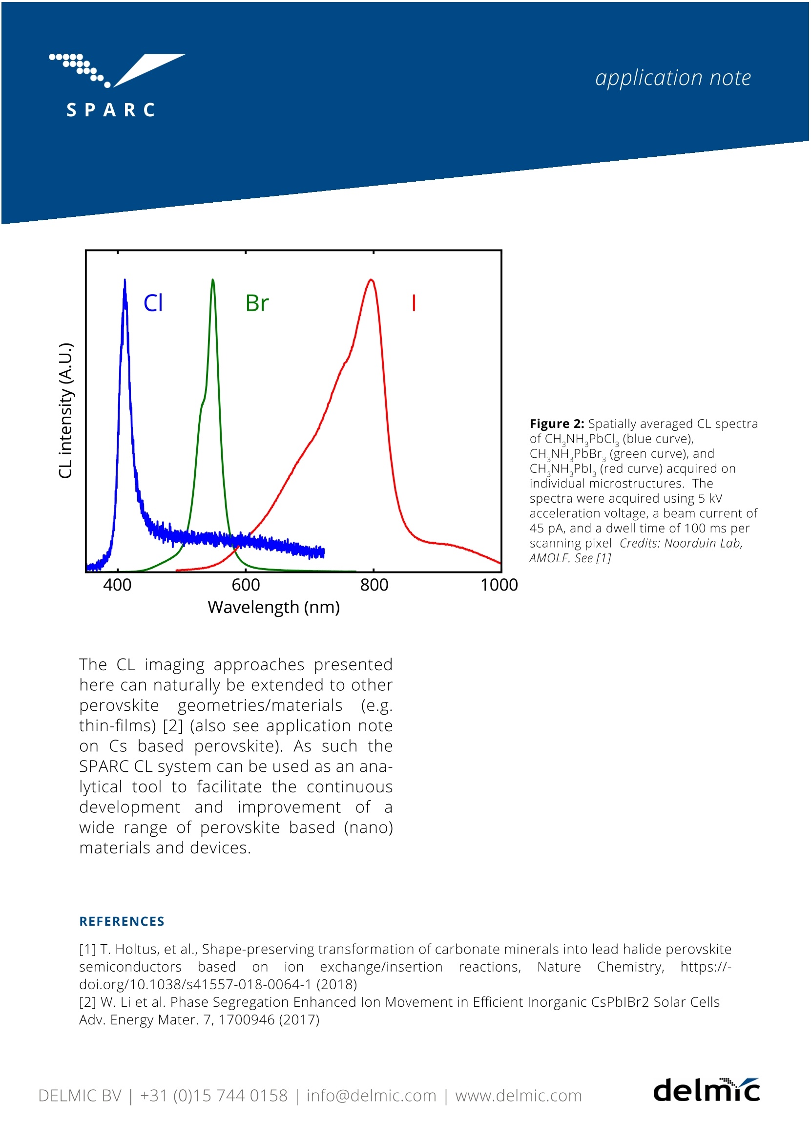
SPAR C SPARC SPAR'C application note Cathodoluminescence lmaging ofThree-Dimensional Methylammonium Lead-Halide Perovskite Structures delnc application note Cathodoluminescence lmaging ofThree-Dimensional MethylammoniumLead-Halide Perovskite Structures Methylammonium lead halide perovskitematerials have gained significant interestdue to their exceptional performance insolar cell, light-emitting diode, laser, andwater splitting devices, while the materi-al synthesis is cheap and very flexible. Inmany cases perovskites are grown inthin-film, platelet, or nanocrystal formbut for some applications more exotic3D shapes would also be of interest. Car-bonate salts, including the well-knownbiomineral calcium carbonate, can beshaped into a large variety of complex3D shapes by using biological or bioin-spiredmineralization processes.Bychemically replacing these carbonatesalts with perovskite in a shape preserv-ing process, the versatile optoelectronicproperties of perovskites can be com-bined with the geometrical tunability ofcarbonate salts[1]. Cathodoluminescence (CL) imaging andspectroscopy provides a powerfulmethod to study the optical propertiesof such 3D perovskites structures ondeep-subwavelengthscales.Figure1shows CL intensity maps of complexperovskite structures, derivedfrom synthetically grown carbonate ma-terial (also see technical note on inten-sity mapping). The CL maps show thatthereiIsS (efficient) light emissionthe structures,indicatingthat the conversion into a light emittingperovskite semiconductor was success-ful. CL images were acquired on a varietyof shapes and perovskite compositionswith different halides in the crystalmatrix (chlorine, bromine, and iodine) asshown in Figure 1. application note c d 10 um 10 pm Figure 1: CL intensity maps of synthetically grown 3D perovskite structures acquired with the SPARC CL system. Imagesshow (a) spiral, (b) trumpet, and (c) spiked-coral shapes of CHNH PbBr. (d) CHNHPbCl, coral shape. (e) Field ofCH,NH Pbl vase shapes. The colors chosen for the color scale represent the emission range of the measured cathodo-luminescence (see Figure 2), with lighter colors corresponding to higher emission intensities. The CL maps wereacquired at 5 kV acceleration voltage, a beam current of 45 pA, and a pixel dwell time of 100 ps per pixel. Credits: Noor-duin Lab, AMOLF. See [1]. Figure 2 shows CL spectra (also see tech-nical note on hyperspectral imaging)acquired on microstructures with differ-ent perovskite compositions, similar tothe structures shown in Figure 1. Asexpected the main emission peak posi-tion strongly depends on which halide isincluded in the perovskite crystal (420,550, and 800 nm for Cl, Br, and I respec-tively), demonstrating that CL can tbeeffectively used to (locally) determine thespectral emissioncharacteristics ofdifferent perovskite compounds. It is known that methylammonium per-ovskite materials are more fragile com-pared to some of their fully inorganiccounterparts. Nevertheless, high-qualityCL maps could be acquired on the struc-tureswithout significant degradation,demonstrating that this imagingapproach is not too destructive for per-ovskites. Figure 2: Spatially averaged CL spectraof CH,NH,PbCl, (blue curve),CH,NHPbBr, (green curve),andCH,NH,Pbl (red curve) acquired onindividual microstructures. Thespectra were acquired using 5 kVacceleration voltage, a beam current of45 pA, and a dwell time of 100 ms perscanning pixel Credits: Noorduin Lab,AMOLF. See [1] Wavelength (nm) The CL imaging approaches presentedhere can naturally be extended to otherperovskite: geometries/materials(e.g.thin-films) [2] (also see application noteon Cs based perovskite). As such theSPARC CL system can be used as an ana-lytical tool to facilitate the continuous'ysdevelopment andimprovement ofwide range of perovskite based (nano)materials and devices. ( REFERENCES ) [1] T. Holtus, et al., Shape-preserving transformation of carbonate minerals into lead halide perovskitesemiconductors based(on ionexchange/insertion reactions, NatureChemistry, https://-doi.org/10.1038/s41557-018-0064-1(2018) [2] W. Li et al. Phase Segregation Enhanced Ion Movement in Efficient Inorganic CsPblBr2 Solar CellsAdv. Energy Mater. 7, 1700946 (2017) DELMIC B.V. is a company based in Delft, the Netherlandsthat produces correlative light and electron microscopysolutions. DELMIC's systems cater to a broad range of researchersin fields ranging from nanophotonics to cell biology. The SPARC is a high-performance cathodoluminescencedetection system produced by DELMIC. The system isdesigned to optimally collect and detect cathodolumines-cence emission, enabling fast and sensitive materialcharacterization at the nanoscale. For questions regarding this note, contact our SPARC Applica-tion Specialist Toon Coenen at: coenen@delmic.com For more resources, see: delmic.com/resources For more information on the SPARC, visit: delmic.com/sparc delnuc delmic.com Kanaalweg,4 2628 EB Delft The Netherlands delmicDELMIC BV+()info@delmic.comwww.delmic.com delmicinfo@delmic.comwww.delmic.com Methylammonium lead halide perovskitematerials have gained significant interestdue to their exceptional performance in solar cell, light-emitting diode, laser, and water splitting devices, while the materi-al synthesis is cheap and very flexible. Inmany cases perovskites are grown inthin-film, platelet, or nanocrystal form but for some applications more exotic 3D shapes would also be of interest. Car-bonate salts, including the well-known biomineral calcium carbonate, can beshaped into a large variety of complex3D shapes by using biological or bioin- spired mineralization processes. Bychemically replacing these carbonatesalts with perovskite in a shape preserv- ing process, the versatile optoelectronicproperties of perovskites can be com-bined with the geometrical tunability of carbonate salts [1].Cathodoluminescence (CL) imaging and spectroscopy provides a powerful method to study the optical properties of such 3D perovskites structures on deep-subwavelength scales. Figure 1 shows CL intensity maps of complex shaped perovskite structures, derivedfrom synthetically grown carbonate material (also see technical note on intensity mapping). The CL maps show that there is (efficient) light emission throughout the structures, indicating that the conversion into a light emitting perovskite semiconductor was success- ful. CL images were acquired on a variety of shapes and perovskite compositions with different halides in the crystal matrix (chlorine, bromine, and iodine) as shown in Figure 1.It is known that methylammonium per- ovskite materials are more fragile com- pared to some of their fully inorganic counterparts. Nevertheless, high-quality CL maps could be acquired on the struc- tures without significant degradation, demonstrating that this imaging approach is not too destructive for per- ovskites.Figure 2 shows CL spectranical note on hyperspectral imaging) acquired on microstructures with differ- ent perovskite compositions, similar to the structures shown in Figure 1. As expected the main emission peak posi- tion strongly depends on which halide is included in the perovskite crystal (420, 550, and 800 nm for Cl, Br, and I respec- tively), demonstrating that CL can be effectively used to (locally) determine the spectral emission characteristics of different perovskite compounds.
确定

还剩3页未读,是否继续阅读?

产品配置单

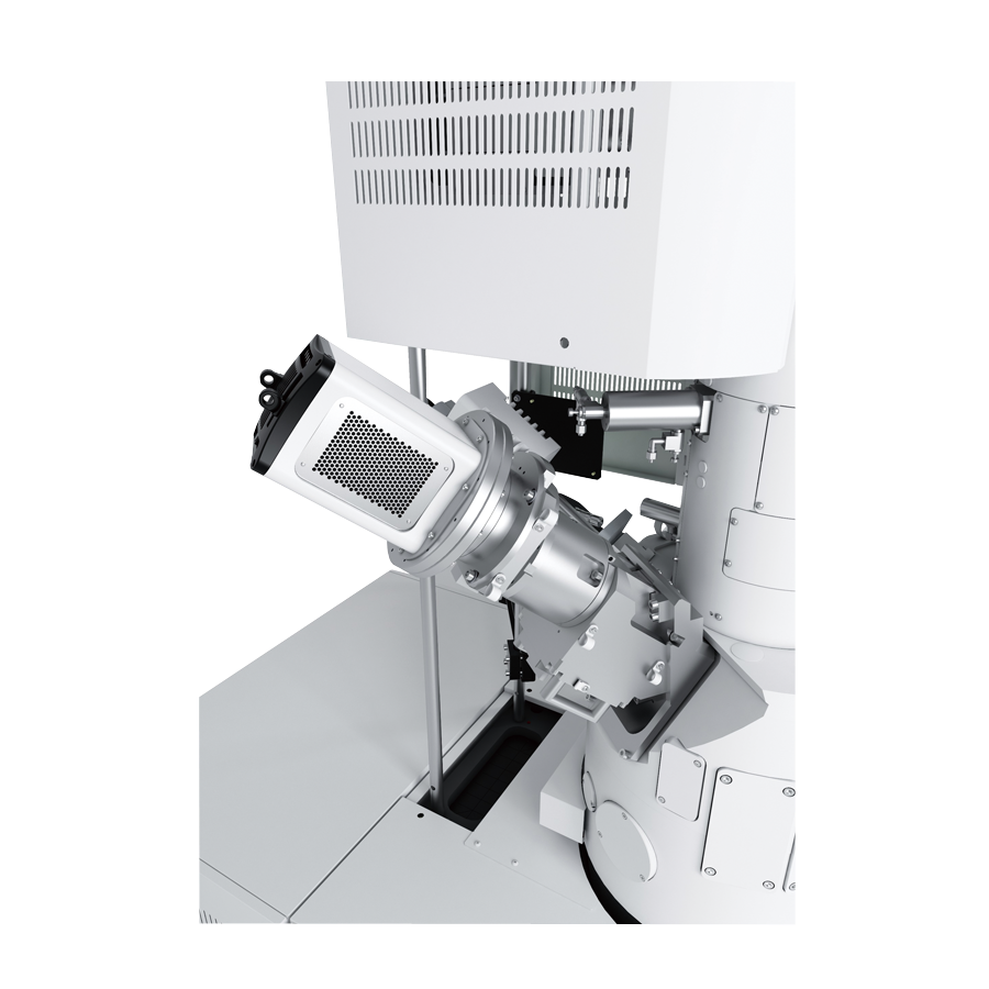
苏州德尓微仪器有限公司为您提供《钙钛矿中形貌检测方案(电镜部件)》,该方案主要用于其他中形貌检测,参考标准--,《钙钛矿中形貌检测方案(电镜部件)》用到的仪器有SPARC -高性能SEM阴极发光成像系统
推荐专场


相关方案
更多