


方案详情
文
椭偏仪是一种无损的薄膜表征方法,它可针对单层或多层光学薄膜给出膜厚、折射率、消光系数、甚至材料的带隙等丰富信息。并可表征膜中的各向异性、渐变、孔隙率等各种不均匀性。本文中,使用椭偏仪表征了TFT-LCD显示器件中透明电极、液晶及a-Si各膜层。分析了透明电极中的渐变层、液晶的各向异性、及a-Si的n型掺杂。
方案详情

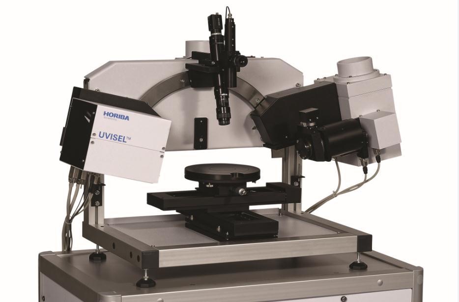
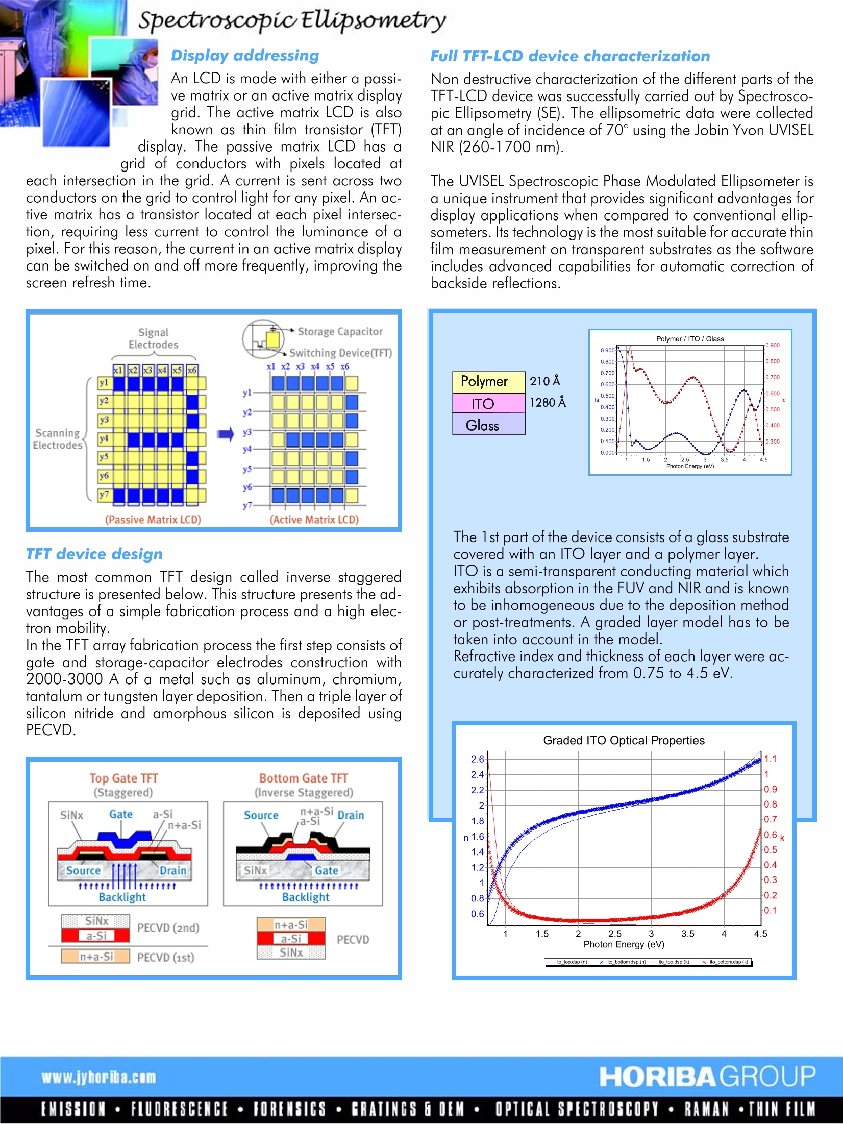
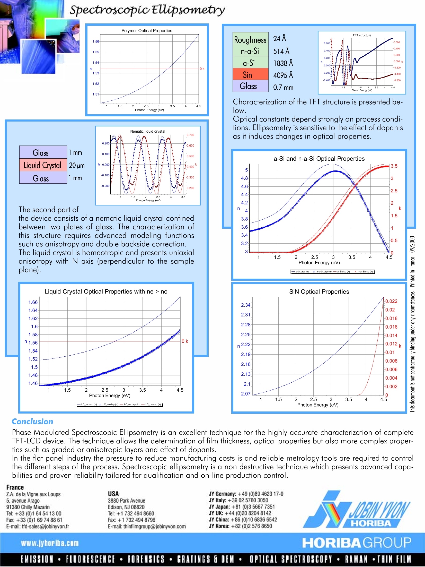
SpectroscopicEUipsometry TFT -LCD Display Melanie Gaillet - Application Scientist - Thin Film Division Most displays in current use employ cathode ray tube (CRT) technology similar to that used inmost television sets. The CRT technology requires a certain distance from the beam projectiondevice to the screen to function. Using other technologies, displays can be much thinner andare known as flat-panel displays. Flat panel display technologies include light-emitting diode(LED), liquid crystal display (LCD) and gas plasma. LED and gas plasma work by lighting up dis-play screen positions based on voltages at different grid intersections. LCDs are categorized asnon-emissive display devices, in that respect they do not produce any form of light. LCDs eitherpass or block light that is reflected from an external light source or provided by a back/side li-ghting system. LCDs require far less energy than LED and gas plasma technologies and are cur-rently the primary technology for notebook and other laptop computers. LCD Structure LCD devices consists of a nematic liquid crystalsandwiched between two plates of glass. In detail,first a sheet of glass is coated with a transparent con-ducting metal oxide film which acts as an electrode.This film can be patterned to form the rows and co-lumns ot a passive matrix display or the individualpixels of an active matrix display. These electrodesare used to set up the voltage across the cell neces-sary for the orientation transition. Next, a polymer alignment layer is applied. This layerundergoes a rubbing process wfhich l narallel microscanic araaves in tehaev efsi lam sTehreisees)S groovegrooves help align the liquid crystal molecules in apreferred direction, with their longitudinal axes pa-rallel to the grooves. The same sheet of glass is pre-pared and once the display has been tilled withliquid crystals, crossed polarizers are applied to theexposed glass surfaces. When an electric field is applied between the twoelectrodes, liquid crystal molecules will react insuch a way as to control light passage. Introduction to liquid Crystal The molecules forming liquid crystals are of-ten characterized by cigar-shaped or elonga-ted molecules.The direction oftheelongation defines the long axis of the mole-afacules. The essential properties ot a liquidcrystal are its optical and electromagneticanisotropy. The manifestation of this propertyat the molecular level is that the long axis ofthe molecules tend to align in a preferred di-rection, that is, they have orientational order.Depending on the type of this orientationalorder, there are a number of distinct phasesof liquid crystals materials : nematic, smecticand cholesteric For displays applications, the most useful arethe nematic and twisted nematic phases. Thenematic phase is characterized by long-ran-ge orientational order. The long molecularaxes possess a preferred orientation, so thaton the average they are positioned parallelto the director. The director field is easily dis-torted by electromagnetic fields or by surfa-ces that have been properly prepared. By introducing a nematic liquid between twosurfaces with the alignment preparation per-pendicular to each other, a peculiar situationis achieved where the director is seen to ro-tate in a regular fashion from one plate toanother as one progresses along the twistaxis. This is known as the 90 degree twistednematic phase that is widely used for liquidcrystal displays. SpectroscopicEUipsometry Display addressing An LCD is made with either a passi-ve matrix or an active matrix displayarid. The active matrix LCD is alsoknown as thin film transistor (TFT) display. The passive matrix LCD has a grid of conductors with pixels located at each intersection in the grid. A current is sent across twoconductors on the grid to control light for any pixel. An ac-tive matrix has a transistor located at each pixel intersec-eation, requiring less current to control the luminance ot apixel. For this reason, the current in an active matrix displaycan be switched on and off more frequently, improving thescreen refresh time. TFT device design The most common TFT design called inverse staggeredstructure is presented below. This structure presents the ad-vantages ot a simple tabrication process and a high elec-tron mobility. In the TFT array fabrication process the first step consists ofgate and storage-capacitor electrodes construction with2000-3000 A of a metal such as aluminum, chromium,tantalum or tungsten layer deposition. Then a triple layer ofsilicon nitride and amorphous silicon is deposited usingPECVD. Full TFT-LCD device characterization Non destructive characterization of the different parts of theTFT-LCD device was successfully carried out by Spectrosco-pic Ellipsometry (SE). The ellipsometric data were collectedat an angle of incidence of 70° using the Jobin Yvon UVISELNIR (260-1700 nm). The UVISEL Spectroscopic Phase Modulated Ellipsometer isa unique instrument that provides significant advantages fordisplay applications when compared to conventional ellip-someters. Its technology is the most suitable for accurate thinfilm measurement on transparent substrates as the softwareincludes advanced capabilities for automatic correction ofbackside reflections. The 1st part of the device consists of a glass substratecovered with an ITO layer and a polymer layer. ITO is a semi-transparent conducting material whichexhibits absorption in the FUV and NIR and is knownto be inhomogeneous due to the deposition methodor post-treatments. A gradedlcayer model has to betaken into account in the model. Retractive index and thickness ot each layer were ac-curately characterized from 0.75 to 4.5 eV. Glass 1mm Glass 1mm The second part of the device consists of a nematic liquid crystal confinedbetween two plates of glass. The characterization ofthis structure requires advanced modeling functionssuch as anisotropy and double backside correction. The liquid crystal is homeotropic and presents uniaxialanisotropy with N axis (perpendicular to the sampleplane). Roughness 24A n-a-Si 514 A a-Si 1838A Sin 4095A Glass 0.7 mm Characterization of the TFT structure is presented be-lOW. Optical constants depend strongly on process condi-tions. Ellipsometry is sensitive to the etfect of dopantsas it induces changes in optical properties. '号吕 Conclusion Phase Modulated Spectroscopic Ellipsometry is an excellent technique for the highly accurate characterization of completeTFT-LCD device. The technique allows the determination of film thickness, optical properties but also more complex proper-ties such as graded or anisotropic layers and effect of dopants. In the flat panel industry the pressure to reduce manufacturing costs is and reliable metrology tools are required to controlthe different steps of the process. Spectroscopic ellipsometry is a non destructive technique which presents advanced capa-bilities and proven reliability tailored for qualification and on-line production control. France 5. avenue Arago Z.A. de la Vigne aux LoupsUSAJY Germany: +49 (0)89 4623 17-03880 Park AvenueJY Italy:+39 02 5760 305091380 Chilly MazarinEdison,NJ 08820JY Japan: +81 (0)356677351Tel: +33 (0)1 64 54 13 00Tel: +1 7324948660JY UK: +44 (0)20 8204 8142Fax: +33 (0)1 69 74 88 61Fax: +1 732 494 8796JY China: +86 (0)106836 6542E-mail: tfd-sales@jobinyvon.frE-mail: thinfilmgroup@jobinyvon.comJY Korea:+82 (0)2 576 8650 EMISSION·FLUORESCENCE·FORENSICS·tCRATINGS EOEM·OPTICAL SPEGTROSCOPY·RAMAN·THIN FILM 椭偏光谱仪在TFT-LCD显示器中的应用椭偏仪是一种无损的薄膜表征方法,它可针对单层或多层光学薄膜给出膜厚、折射率、消光系数、甚至材料的带隙等丰富信息。并可表征膜中的各向异性、渐变、孔隙率等各种不均匀性。本文中,使用椭偏仪表征了TFT-LCD显示器件中透明电极、液晶及a-Si各膜层。分析了透明电极中的渐变层、液晶的各向异性、及a-Si的n型掺杂。
确定
还剩1页未读,是否继续阅读?

产品配置单

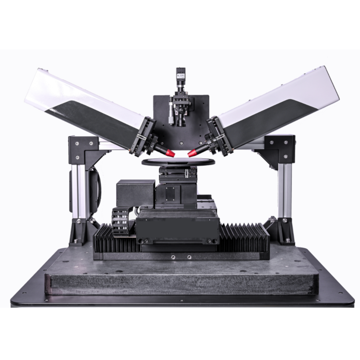
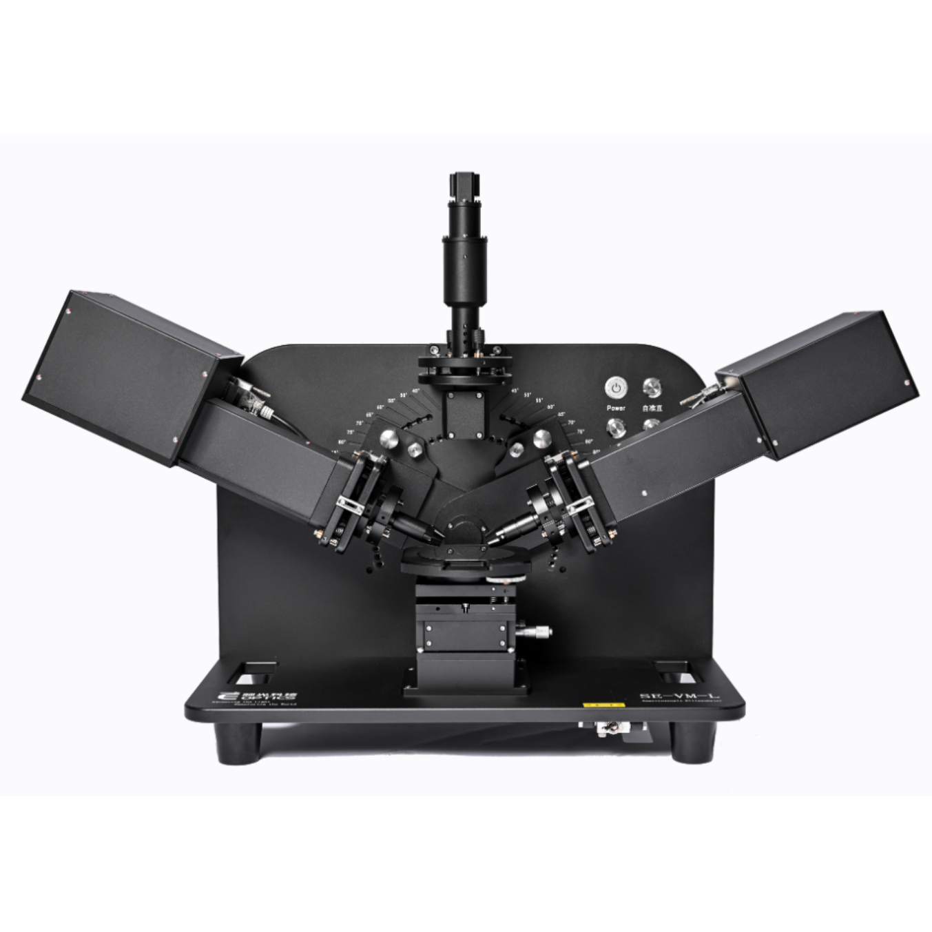
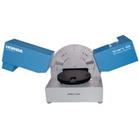
上海巨纳科技有限公司为您提供《氧化铝中痕量元素检测方案(椭偏仪)》,该方案主要用于铝中含量分析检测,参考标准--,《氧化铝中痕量元素检测方案(椭偏仪)》用到的仪器有HORIBA Smart SE智能型多功能椭偏仪
推荐专场