


方案详情
文
通过高分子网状模板沉积不同薄膜材料(Au, Cu, Ni, SiO2, poly(C8H4F4))获得周期有序微格结构,其密度在0.5 mg/cm3 to 500 mg/cm3之间。以压力法测得杨氏模量和强度,并且进行了密度定标。在低相对密度的情况下,观察到与微格材料无关的50%或更高的压力应变恢复。一个分析模型的预测了在可恢复性“伪超弹性”与不可恢复塑性形变之间的转换关系,并适合所有研究材料。此次研究的材料在储能应用,可展开结构,声,冲击,振动阻尼研究方面有着很高的关注度。
方案详情

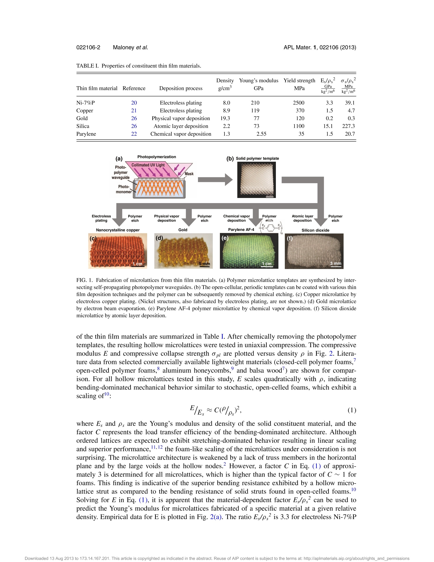
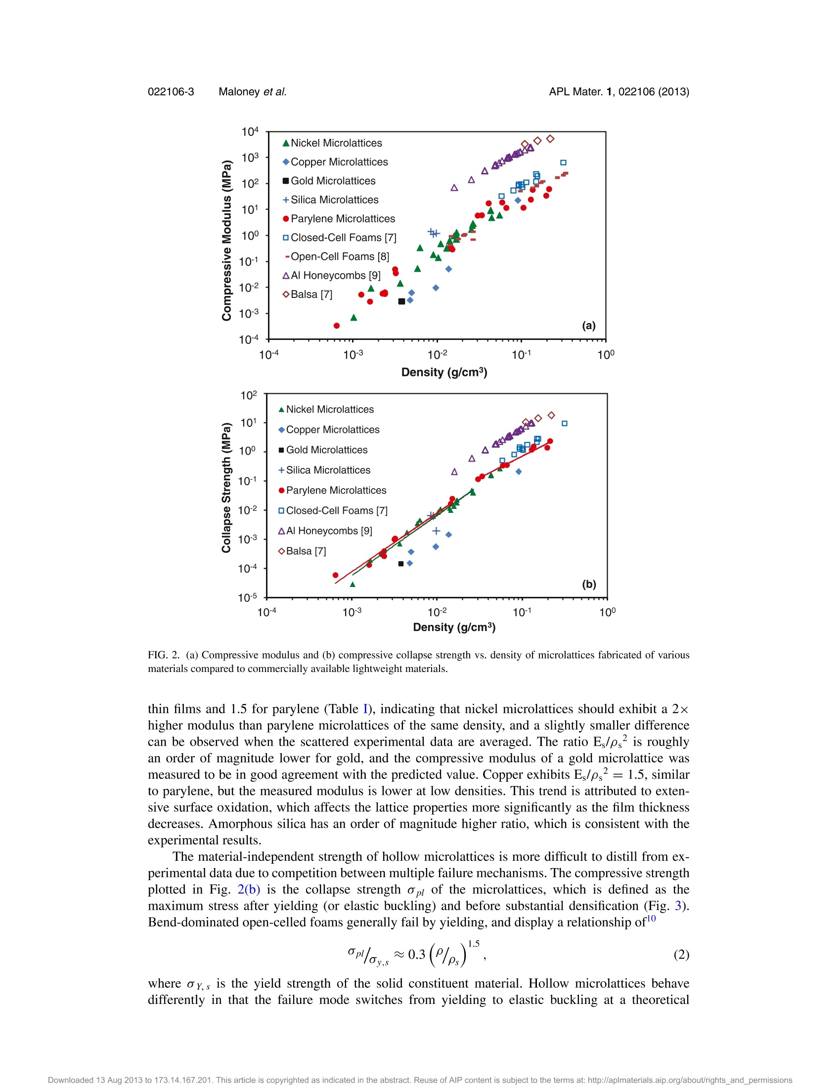
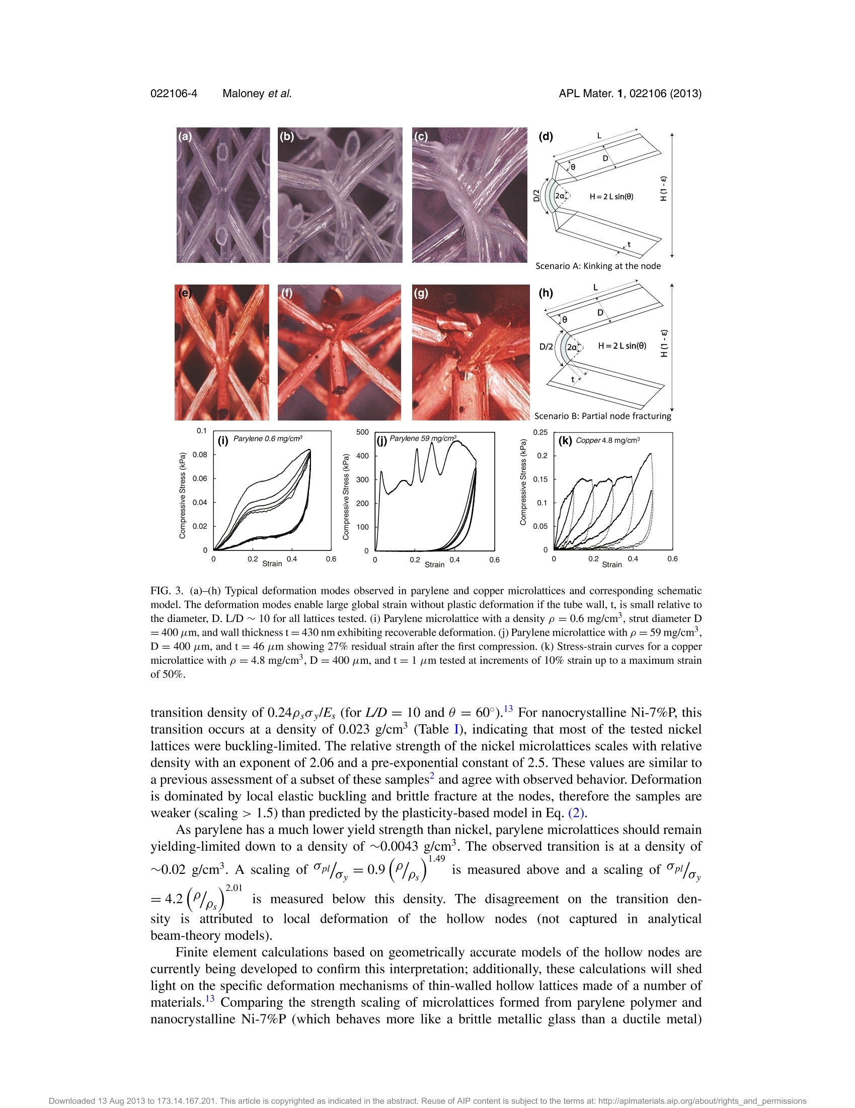
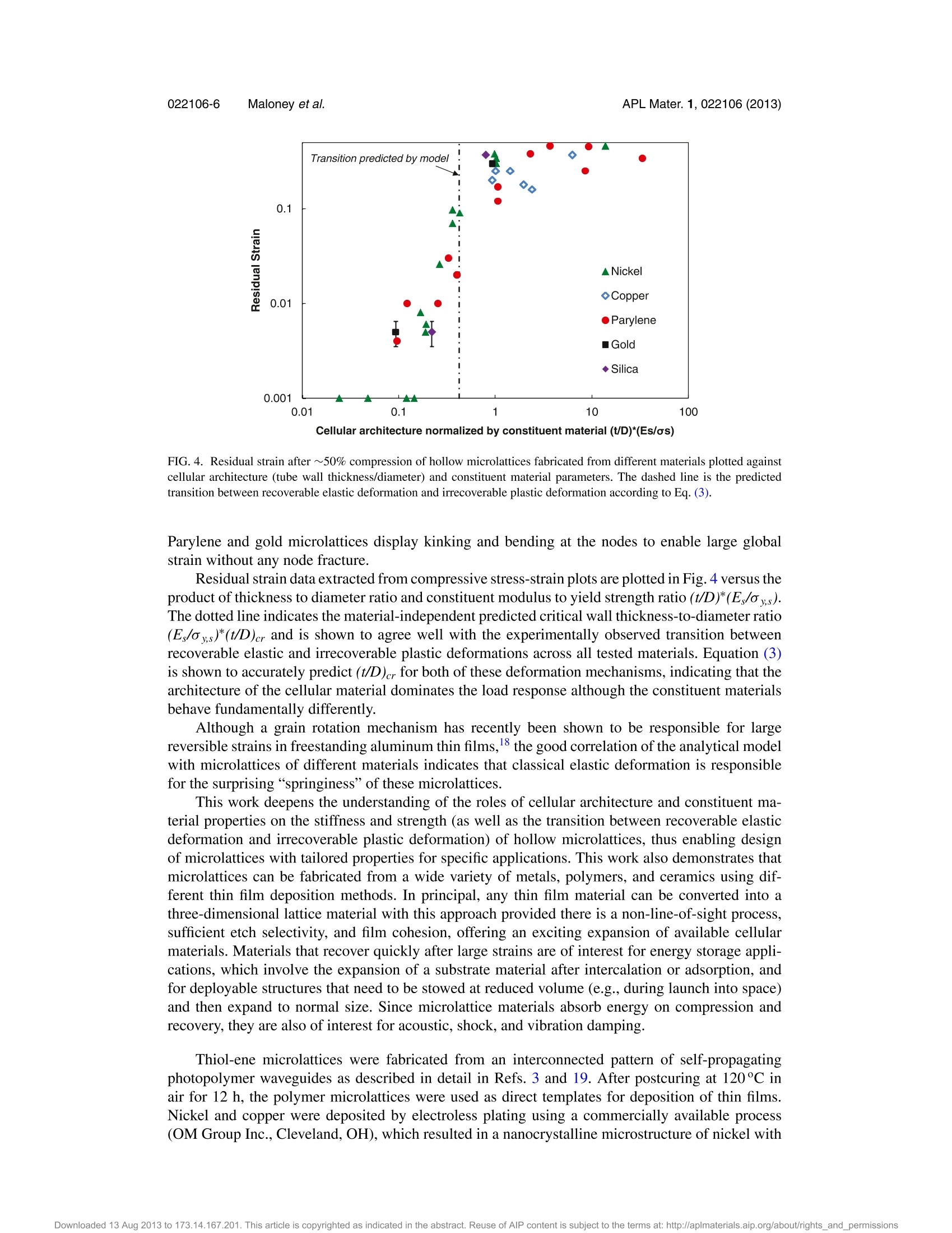
CrossMark 1.5) than predicted by the plasticity-based model in Eq.(2). As parylene has a much lower yield strength than nickel, parylene microlattices should remainyielding-limited down to a density of ~0.0043 g/cm3. The observed transition is at a density of1.49~0.02 g/cm’. A scaling of pl/o=0.9(/)is measured above and a scaling of pl/=4.2(P/)201 is sm meeaassured below this density. The disagreement on the transition den-sity is aattributed to local deformation of the hollow nodes (not captured in analyticalbeam-theory models). Finite element calculations based on geometrically accurate models of the hollow nodes arecurrently being developed to confirm this interpretation; additionally, these calculations will shedlight on the specific deformation mechanisms of thin-walled hollow lattices made of a number ofmaterials.13 Comparing the strength scaling of microlattices formed from parylene polymer andnanocrystalline Ni-7%P (which behaves more like a brittle metallic glass than a ductile metal) demonstrates that cellular architecture has as much impact on the mechanical performance ofmicrolattices as the constituent material properties. For the copper, gold, and silica microlattices,no conclusions about the trends of strength vs. density can be drawn from the limited experimentaldata, which fall close to the transition densities. The nanocrystalline copper and silica samplesfailed by buckling and brittle fracture; gold microlattices showed extensive buckling and kinking butlittle fracture. The order-of-magnitude lower strength of the nanocrystalline copper microlattices ascompared to Ni-7%P is consistent with the 8.4× lower ratio oy/ps2, the material-dependent scalingfactor in the low-density regime. Silica shows a 5.8x higher oy/ps ratio than Ni-7%P, but thestrength of the measured samples was similar or lower than Ni-7%P, presumably due to the muchlower failure strength (~0.1oy) dictated by the low fracture toughness of glass. A model has been developed which predicts the ratio of wall thickness t to strut diameter D at thetransition between recoverable elastic and irrecoverable plastic deformation.The model assumesthat large strains in microlattices are enabled by rotation of the bars about thin ligaments in theproximity of the nodes, generated either by kinking (local buckling) or partial node fracture (Fig. 3).As the ligaments have thicknesses similar to the bar wall thickness (in the 100 nm-50 um range),large rotations are possible without introducing plastic strains. The critical wall thickness at whichplastic deformation would commence can be expressed as where 8max is the maximum global strain the microlattice experiences, and 0 is the truss angle inradians. Figure 3 explores the two deformation mechanisms by comparing deformation of paryleneand copper microlattices. The deformation starts at the nodes and the nodes play a critical rolein how the deformation continues. A node of a parylene microlattice is shown in Fig. 3(a), whileFig. 3(b) shows this node after the lattice has been compressed by approximately 50%. Kinking andbending is observed but the parylene thin film does not fracture. Large strain is known to inducecrystallization in polymers, creating micron-size grains that scatter light much more efficientlythan the amorphous polymer material (also referred to as crazing). Localized deformation of thebulk parylene is indicated by small areas of white discoloration in a close-up picture of the node(Fig. 3(c)), but most of the deformed parylene stays clear, demonstrating that the lattice withstandslarge strain by kinking at the node and bending. By contrast, the copper lattice fractures at thenode, while the struts stay intact (Figs. 3(f) and 3(g)). The struts do not fracture completely and theremaining ligaments can bend and withstand large global strain. The schematics for the deformationmodes in Figs. 3(d) and 3(h) are simplified to enable calculation of the critical ratio of wall thicknessto lattice member diameter for the transition between recoverable elastic and irrecoverable plasticdeformations (Eq. (3)).Nanocrystalline copper and silica microlattices display partial node fracture:the same deformation mechanism previously observed in nanocrystalline nickel microlattices.2 Cellular architecture normalized by constituent material (t/D)*(Es/os) FIG. 4. Residual strain after ~50% compression of hollow microlattices fabricated from different materials plotted againstcellular architecture (tube wall thickness/diameter) and constituent material parameters. The dashed line is the predictedtransition between recoverable elastic deformation and irrecoverable plastic deformation according to Eq. (3). Parylene and gold microlattices display kinking and bending at the nodes to enable large globalstrain without any node fracture. Residual strain data extracted from compressive stress-strain plots are plotted in Fig. 4 versus theproduct of thickness to diameter ratio and constituent modulus to yield strength ratio (t/D)*(E/oy,s).The dotted line indicates the material-independent predicted critical wall thickness-to-diameter ratio(E,/ay,s)*(t/D)cr and is shown to agree well with the experimentally observed transition betweenrecoverable elastic and irrecoverable plastic deformations across all tested materials. Equation (3)is shown to accurately predict (t/D)cr for both of these deformation mechanisms, indicating that thearchitecture of the cellular material dominates the load response although the constituent materialsbehave fundamentally differently. Although a grain rotation mechanism has recently been shown to be responsible for largereversible strains in freestanding aluminum thin films, 8 the good correlation of the analytical modelwith microlattices of different materials indicates that classical elastic deformation is responsiblefor the surprising “springiness”of these microlattices. This work deepens the understanding of the roles of cellular architecture and constituent ma-terial properties on the stiffness and strength (as well as the transition between recoverable elasticdeformation and irrecoverable plastic deformation) of hollow microlattices, thus enabling designof microlattices with tailored properties for specific applications. This work also demonstrates thatmicrolattices can be fabricated from a wide variety of metals, polymers, and ceramics using dif-ferent thin film deposition methods. In principal, any thin film material can be converted into athree-dimensional lattice material with this approach provided there is a non-line-of-sight process,sufficient etch selectivity, and film cohesion, offering an exciting expansion of available cellularmaterials. Materials that recover quickly after large strains are of interest for energy storage appli-cations, which involve the expansion of a substrate material after intercalation or adsorption, andfor deployable structures that need to be stowed at reduced volume (e.g., during launch into space)and then expand to normal size. Since microlattice materials absorb energy on compression andrecovery, they are also of interest for acoustic, shock, and vibration damping. Thiol-ene microlattices were fabricated from an interconnected pattern of self-propagatingphotopolymer waveguides as described in detail in Refs. 3 and 19. After postcuring at 120°C inair for 12 h, the polymer microlattices were used as direct templates for deposition of thin films.Nickel and copper were deposited by electroless plating using a commercially available process(OM Group Inc., Cleveland,OH), which resulted in a nanocrystalline microstructure of nickel with 7 wt.% phosphorous with a grain size of 7 nmand pure copper with a grain size of ~10 nm,respectively, see Ref. 1 for details. Parylene AF4, a fluorinated poly(p-xylylene) polymer (seeFig. 1) was deposited by chemical vapor deposition by Specialty Coating SystemsTM, Inc. Di-para-xylylene dimer was vaporized at 150°C and 1 Torr, pyrolyzed to the monomer at 600°℃ and 0.5Torr and then deposited as polymer at 25C and 0.1 Torr.22,23 Silica was deposited as an amorphous thin film by ALD by Arradiance Inc. in Sudbury, Mas-sachusetts. Tris(tert-butoxy)silanol precursor was used at a temperature of 95°C and deposited at150℃ in a GEMStar@ system with the catalysis of trimethylaluminum, which resulted in a fastgrowth rate of approximately 10 nm/cycle comparable to reports in the literature.24,25 Gold was deposited as crystalline thin film by electron beam evaporation using a CHA IndustriesMark 50 electron beam evaporator. A rotary, 3-dome planetary fixture was used to continuouslychange the microlattice’s angle with respect to the evaporant stream, and the microlattice wasflipped over halfway through the deposition to improve coverage. By selecting a microlattice withless cells across the thickness and a more open structure (Fig. 1) non-uniformities in the gold filmthickness could be minimized. After deposition of the different thin films, the top and bottom surfaces of each microlatticewere sanded to expose the underlying polymer. The polymer was then chemically etched in a basesolution (1.5M NaOH in 50% H20/50% methanol at 60°C), creating the hollow microlattices shownin Fig. 1. The lightest samples were freeze dried after exchanging the NaOH solution to deionizedwater and then to t-butanol in order to avoid collapse on removal from solution. The film thicknesswas measured by cross-sectional scanning electron microscopy (SEM) and verified by comparingmeasured densities with a computer aided design (CAD) model. The compression tests were performed on a servo-electric INSTRON@ 5565 frame. The dis-placement rate was 0.01 mm/s for loading and unloading, and microlattices of similar dimensionsas shown in Fig. 1 were tested between compression platens without attachment. The loads weremeasured by a SENSOTEC@ load cell with a range of 250 N or an INSTRON load cell with arange of 500 N, and the displacements were measured by an Electronic Instrument Research laserextensometer (Ref. 26). This investigation was sponsored by the Defense Advanced Research Projects Agency underthe Materials with Controlled Microstructural Architecture program managed by J. Goldwasser(Contract No. W91CRB-10-0305). The authors would like to thank A. Sorensen and M. Allenby(HRL Laboratories, LLC) for help with sample preparation and testing. ( T . A. S c haedler, A. J. Jacobsen, A . Torrents, A. E. Sorensen, J. Lian, J. R. G r eer, L. V a ldevit, and W . B. Carter, S c ie n ce 334,962-965 (2011 ) . ) ( A. T o rrents, T . A. Schaedler, A. J. Jacobsen, W. B . Carter, and L . Valdevi t , Ac t a Mate r . 60,3511-3523(2012). ) ( A. J. Jacobsen, W . B. Carter, and S. Nutt, Ad v . Mater. 19, 3892-3896 ( 2007). ) ( “C. S. Roper, Int . J . H ea t Fluid Flo w 32( 1 ), 239-248(2011). ) ( K. J. M a loney, K. D. Fink, T. A. Schaedler, J. A. Kolodziejska, A. J. Jacobsen, and C. S. Roper, Int . J . H eat M a ss Tr a nsfer 55,2486-2493 (2012). ) ( °A. G . Evans, M . Y. He, V. S. Deshpande, J. W. H ut c hinson, A. J. Jaco b sen, and W. B. Carter, Int. J . Im p a c t E ng. 3 7, 9 47-959 (2010). ) ( 7A. G. C Guri t Holding, Core-Cell Datasheets, see h ttp: / /www. gur it . c o m/c o re-mate r i al s-datashe e ts.a s px and h tt p://www. g u r it . co m /files/ d ocu m ents/ba ls aflexwev3pdf. p df. ) ( L. J. G ibson and M. F. Ashby, Pr oc. R . S oc. Lo ndon, S e r. A 38 2,43-59(198 2 ). ) ( Plascore I Inc . PAMG-XR 15 052 A luminum Honeycomb, Da t asheet, 2 012, see h t tp : / /www.pl a score.com/p d f/ Pl a score _ 5052.pdf . ) ( 1 0L. J . Gibson and M. F. A s hby, Ce l lular Solids: St r ucture and Properties (Cambridge University Press, 1997). ) ( 1 1V. S . D eshpande, N. A. Fl e ck, an d M. F. A shby, J. M e c h . Ph y s . Solids 49, 1 747 ( 2001). ) ( A. G. Evans, J. W. Hutchinson, N. A. Fleck, M. F. Ashby, and H. N. G. Wadley, Prog . Ma te r. Sci. 4 6 , 309 (2001). ) ( L . Valdevit, S. W. Godfrey,T. A. Schaedler, A. J.Jacobson, and W. B. Carter,“Compr e ssive strength of hollow microlattices: Experimental characterization, modeling, a nd o ptimal design,"J. M ater. R es. (published o nline). ) ( 1 4J. Zou, J . Liu, A. S. Karakoti, A. Kumar, D . J o ung, Q. Li, S. I. K hondaker, S. Seal, and L. Zhai, AC S N a no 4, 7 2 93 - 7302 ( 2 010). ) ( 15 M. Xu, D. N. Futaba, T. Yamada, M. Yumura, a nd K . Hata, Science 330,1364(2010). ) ( 16 S. B. Hutchens, A. Needleman, and J. R. Greer, J. M ech. P h ys. So l ids 59 ,2227-2237(2011) . ) ( E. J. Kramer, A dv. P olym . S ci. 52-53, 1-56(1983). ) ( 18 S. Kumar, M. T . Alam, and M. A. Haque, J. M i c roele c tromech. Syst . 20( 1 ), 53 (201 1 ). ) 022106-8 Maloney et al. 19 A. J. Jacobsen, W. B. Carter, and S. Nutt, Acta Mater. 55, 6724-6733 (2007). ( 20J. Lian, L. Valdevit, T. A. Schaedler, A. J . Jacobsen, W. Barvosa-Carter, and J. R . G reer, N ano Lett. 1 1, 4118 (2011) ) 2 S.-Y. Chang and T.-K. Chang,J. Appl.Phys. 101,033507(2007). 222J3.刀 J. Licari, Coating Materials for Electronic Applications (Noyes Publications, 2003). 23 Handbook of Plastics, Elastomers and Composites (McGraw Hill, Inc., 2002), Chap. 6. 24D. Hausmann, J. Becker, S. Wang, and R. G. Gordon, Science 298, 402-406(2002). 25 B. B. Burton, M. P. Boleslawski, A. T.Desombre, and S. M. George, Chem. Mater. 20, 7031-7043 (2008). 26 W. D. Callister, Materials Science and Engineering: An Introduction (John Wiley and Sons, Inc., 2000). Downloaded Aug to This article is copyrighted as indicated in the abstract. Reuse of AIP content is subject to the terms at: http://aplmaterials.aip.org/about/rights_and_permissions
确定

还剩7页未读,是否继续阅读?


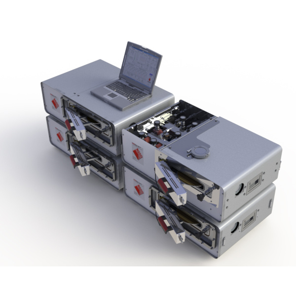
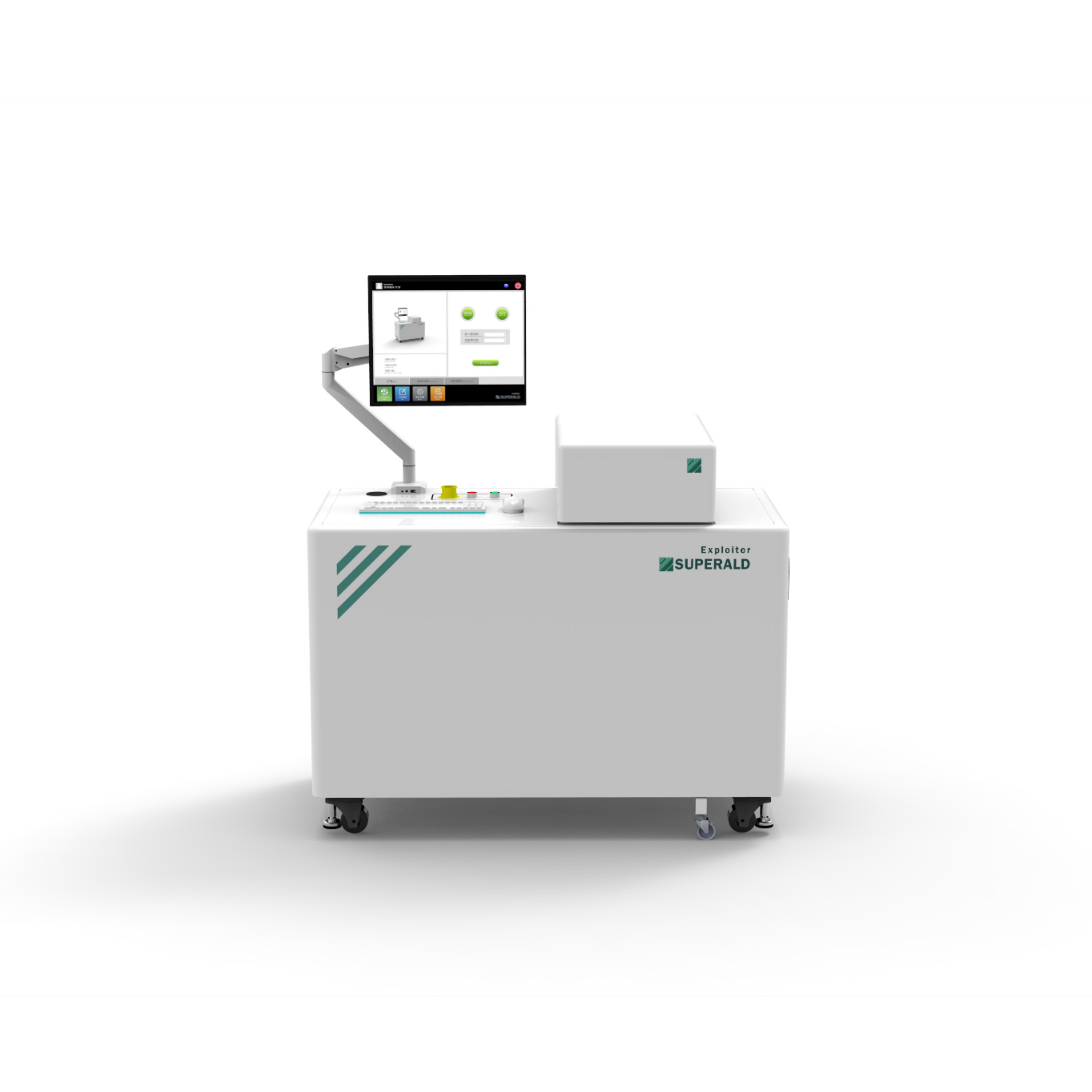
QUANTUM量子科学仪器贸易(北京)有限公司为您提供《Au, Cu等薄膜材料中周期有序微格结构检测方案(原子层沉积)》,该方案主要用于薄膜材料中周期有序微格结构检测,参考标准--,《Au, Cu等薄膜材料中周期有序微格结构检测方案(原子层沉积)》用到的仪器有台式原子层沉积系统
推荐专场

相关方案
更多
该厂商其他方案
更多