


方案详情
文
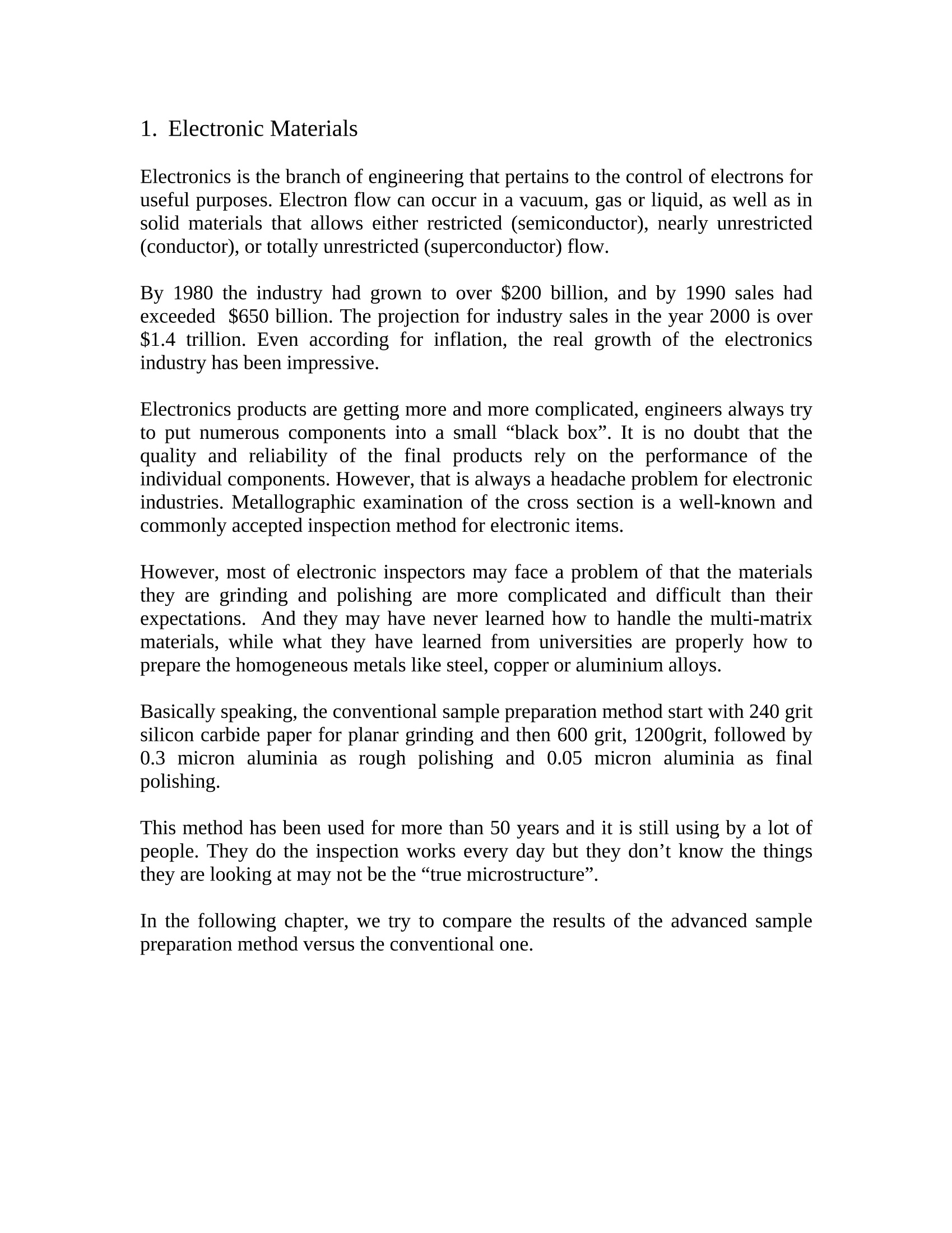
1、电子产品正变得越来越复杂,工程技术人员总是力图将许多部件放在一个小小的“黑匣子” 中。 毫无疑问,最终产品的质量和可靠性取决于每个部件的性能。然而,这也总是电子工业的一个令人头痛的问题。对电子产品的截面进行金相检验是一种众所周知并通常广为接受的检验方法。
然而,大多数电子产品检验员可能面临的一个问题就是他们需要进行磨光和抛光的材料比预期的复杂和困难。而且他们也许从来没有学习过如何去处理多层基体材料,他们在大学学习时只学过如何恰当地制备均匀的材料,例如钢、铜合金或铝合金。
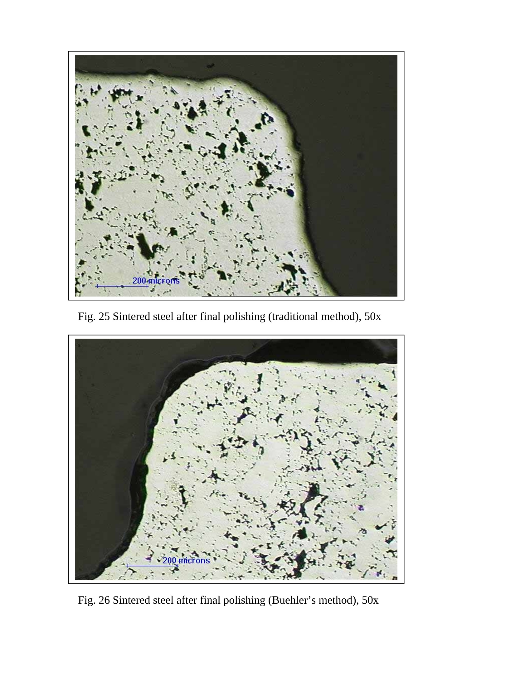
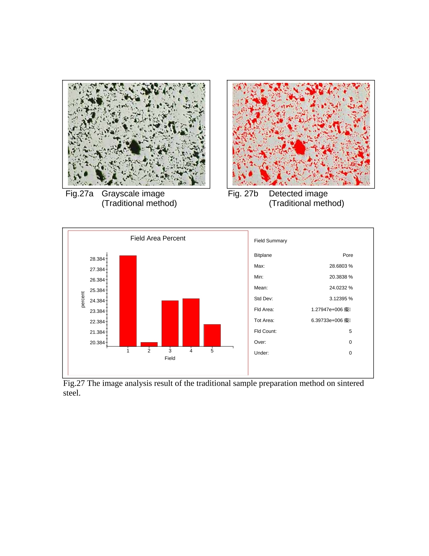
2、烧结钢零件的横截面试样制备好以后, 不难发现在心部仍然有一些孔隙. 孔隙的面积分数也是该烧结钢零件是否合格的一个重要判据. 然而, 如果试样制备的方法不正确, 测出的孔隙面积分数可能更小或更大.
为了评估试样制备方法对试样中孔隙面积分数的影响, 可将一个烧结钢零件切成两块。其中一个面用传统方法制备, 另一个面用Buehler方法制备.
方案详情

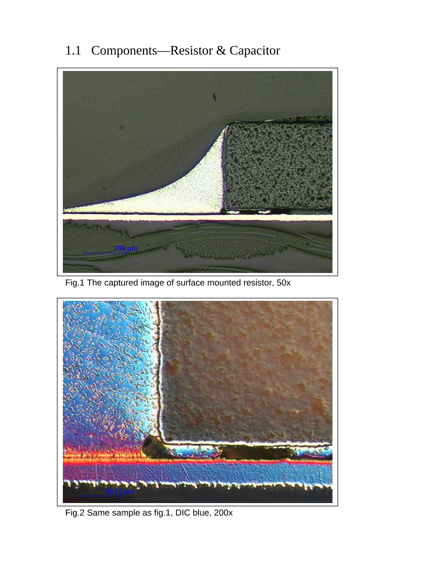
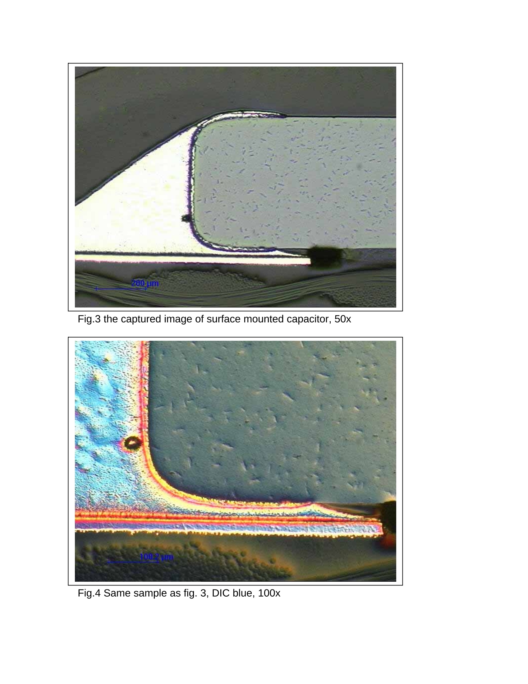
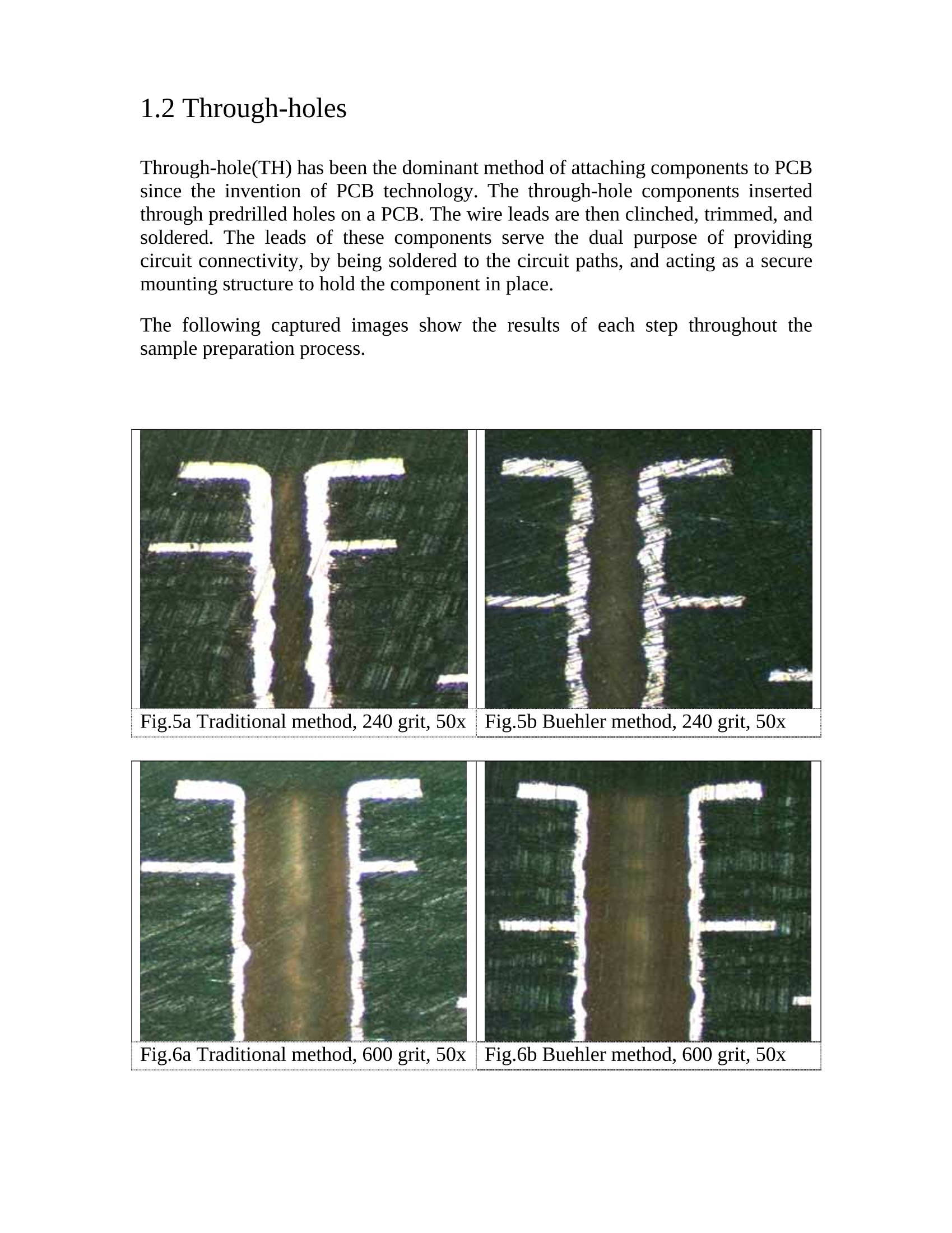
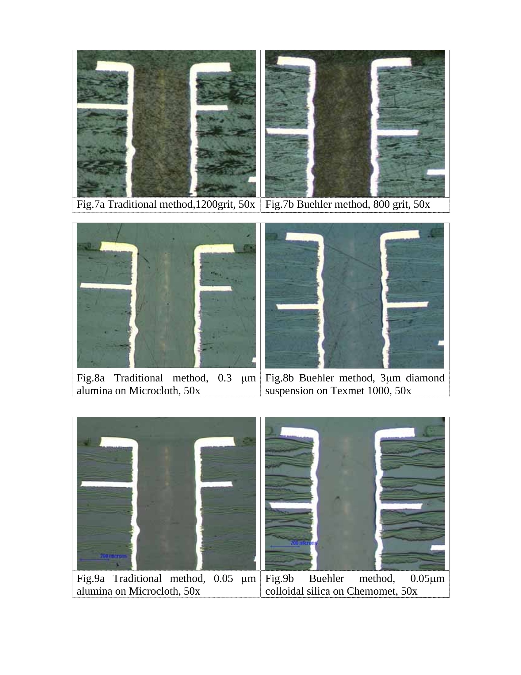
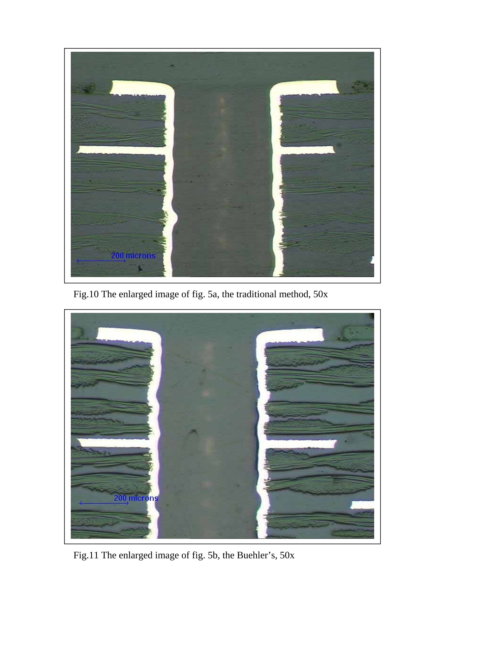
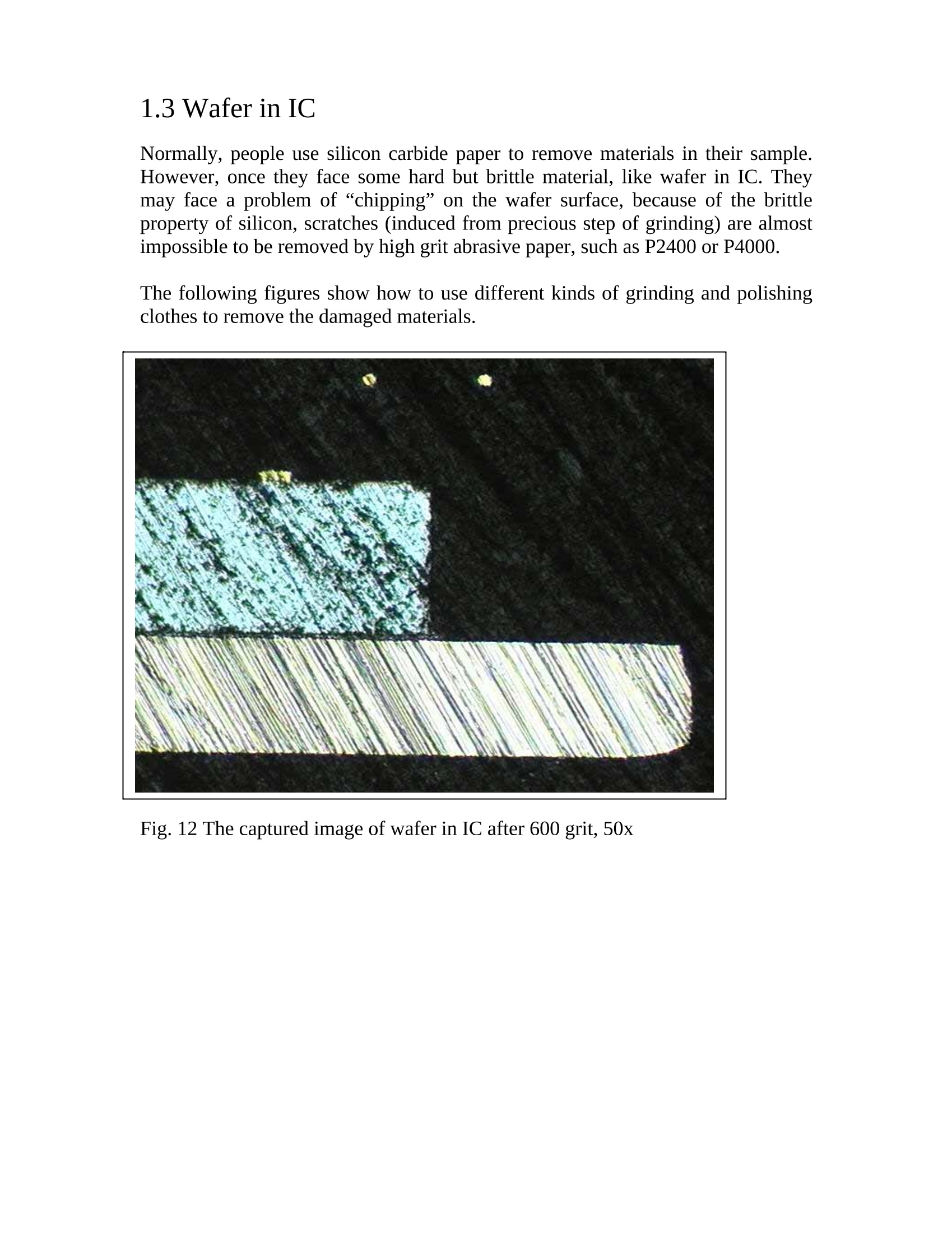
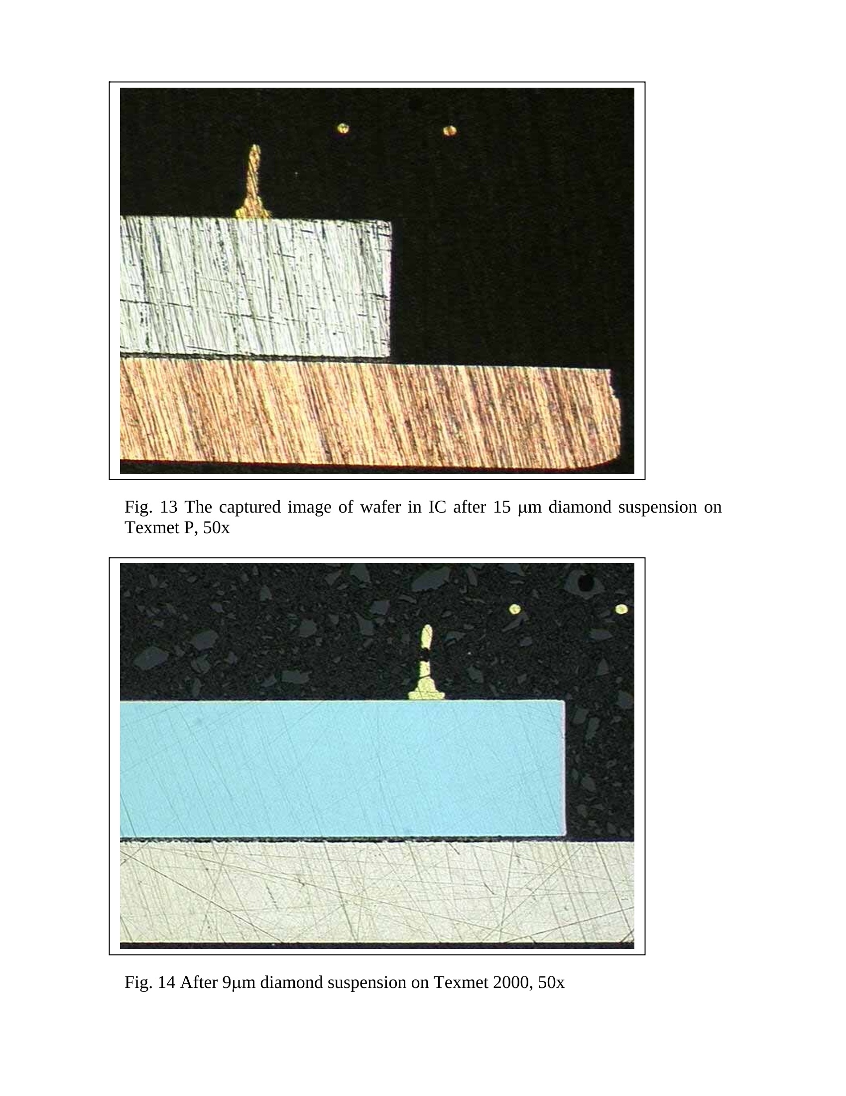
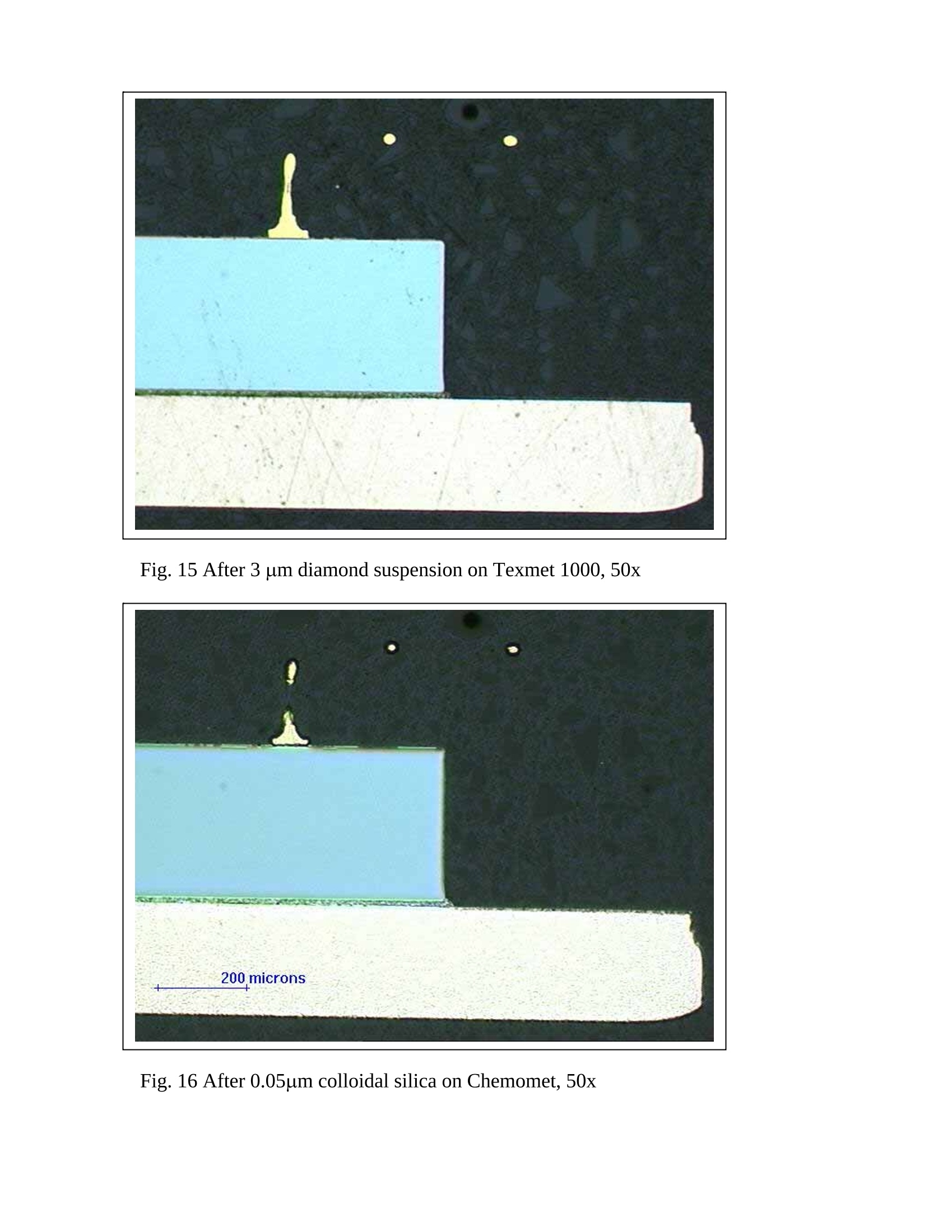
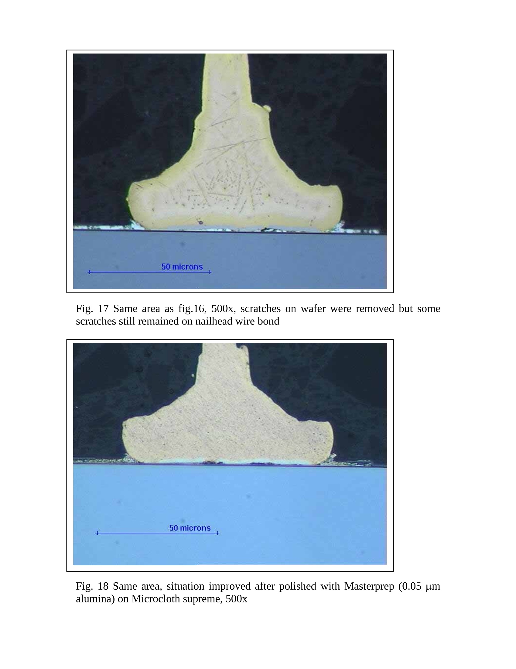
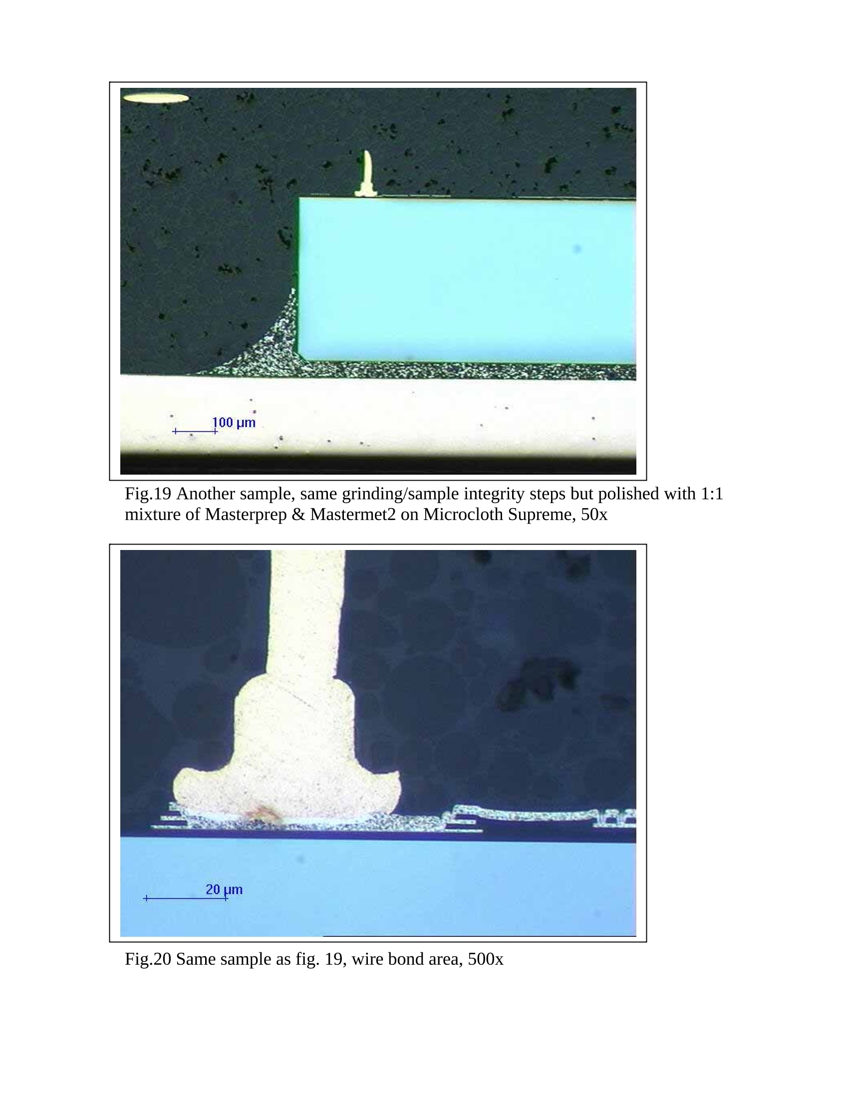
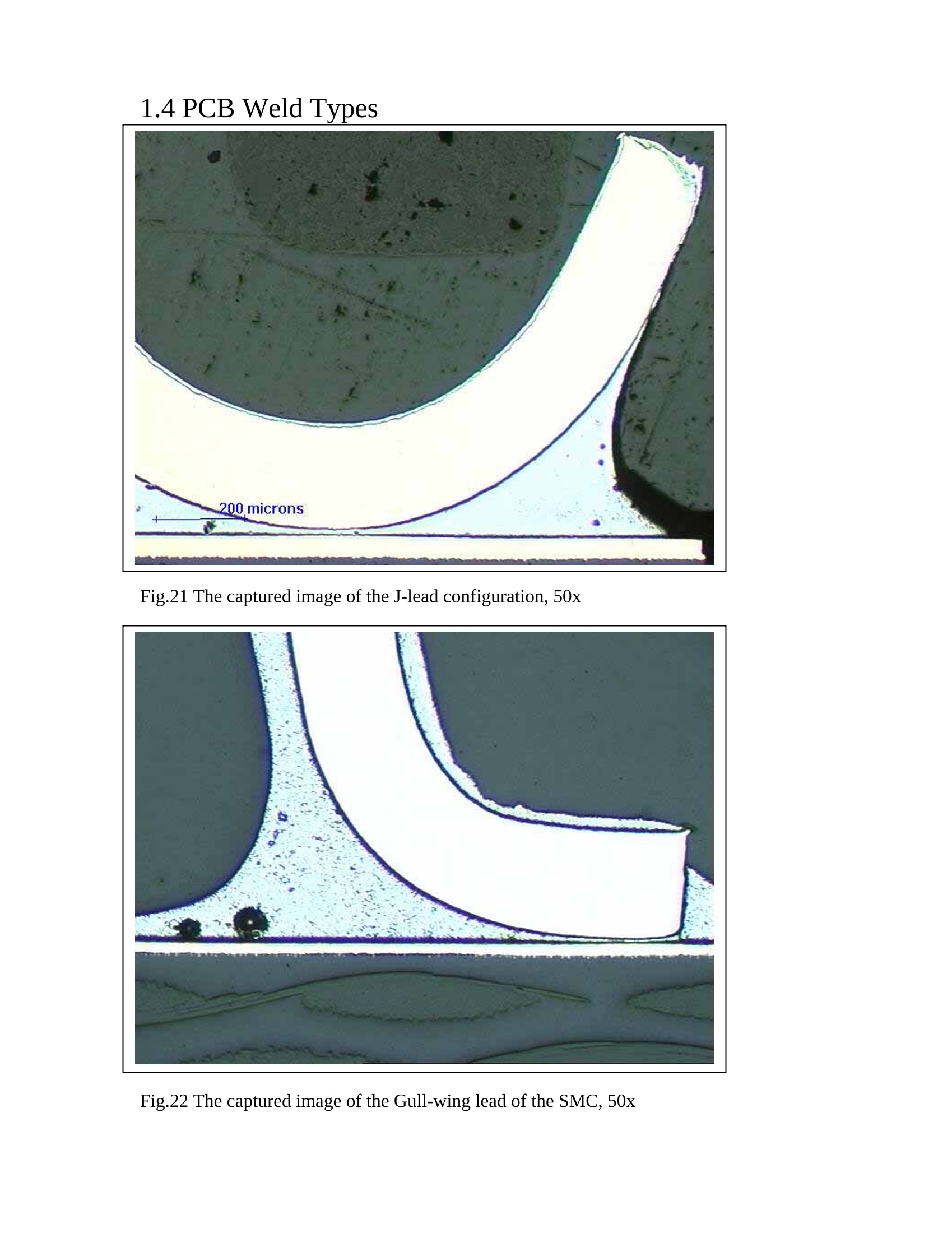
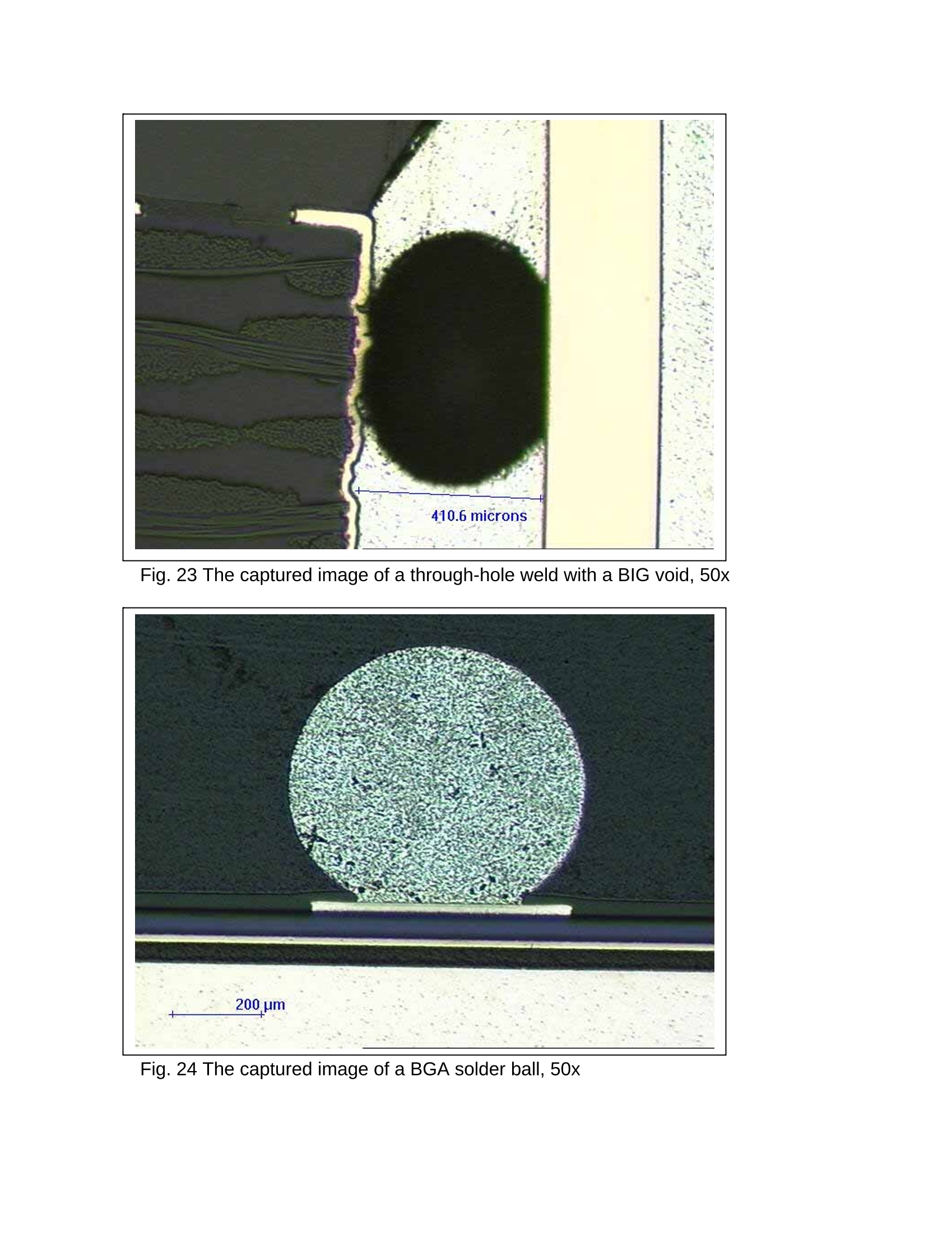
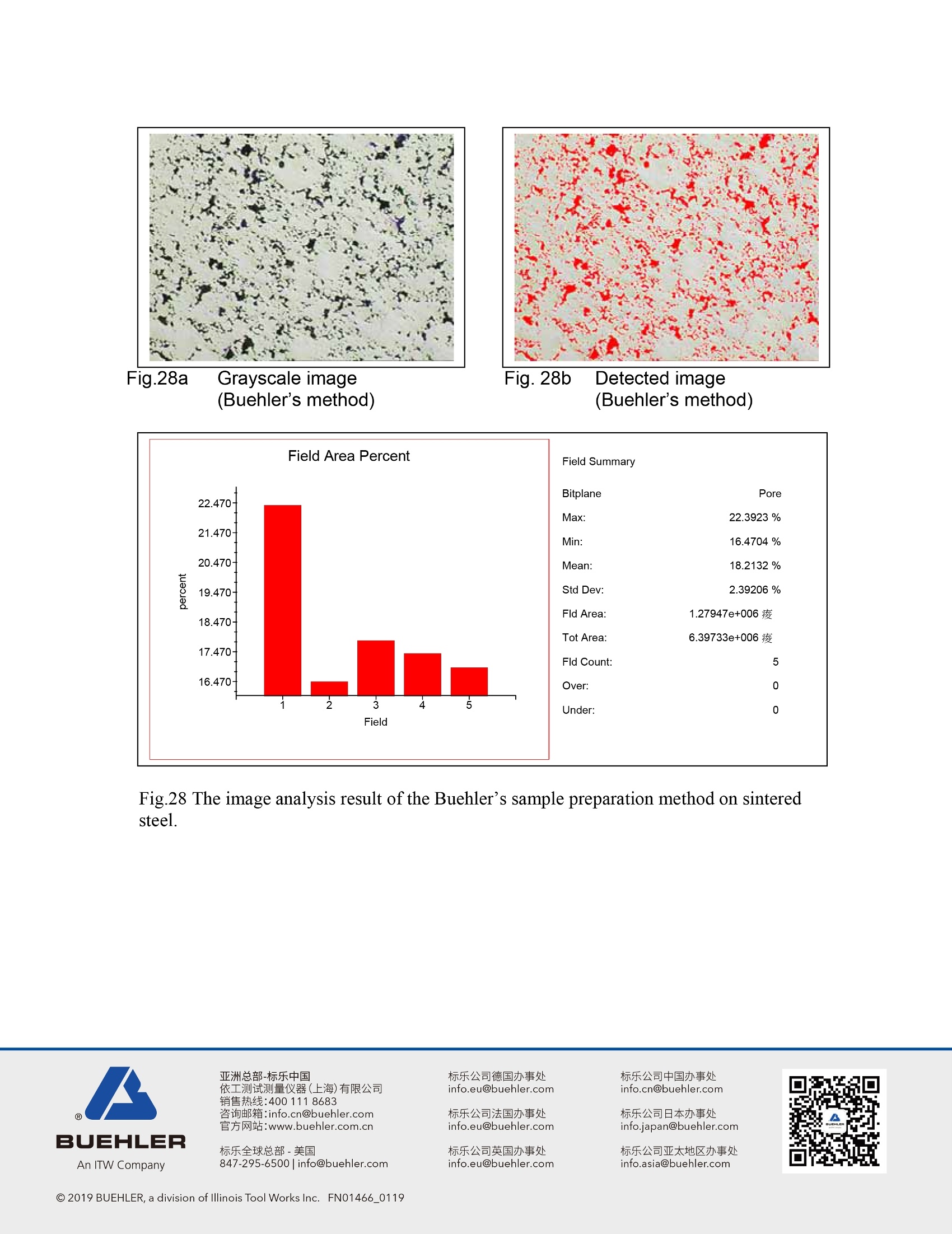
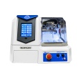
标乐公司亚太地区办事处info.asia@buehler.com标乐公司英国办事处info.eu@buehler.com标乐全球总部-美国847-295-6500|info@buehler.com 2019 BUEHLER, a division of Illinois Tool Works Inc. FN01466_0119 Conventional vs. AdvancedSample Preparation Method 1. Electronic Materials 1.1 Components-Resistor & Capacitor 1.2 PCB Through-hole 1.3 Wafer in Integrated Circuit 1.4 PCB Weld Types 2. Sintered Steel 2.1 Images of different preparation method 2.2 Image analysis results 1. Electronic Materials Electronics is the branch of engineering that pertains to the control of electrons foruseful purposes. Electron flow can occur in a vacuum, gas or liquid, as well as insolid materials that allows either restricted (semiconductor), nearly unrestricted(conductor), or totally unrestricted (superconductor) flow. By 1980 the industry had grown to over $200 billion, and by 1990 sales hadexceeded $650 billion. The projection for industry sales in the year 2000 is over$1.4 trillion. Even according for inflation, the real growth of the electronicsindustry has been impressive. Electronics products are getting more and more complicated, engineers always tryto put numerous components into a small “black box". It is no doubt that thequality and reliability of the final products rely on the performance of theindividual components. However, that is always a headache problem for electronicindustries. Metallographic examination of the cross section is a well-known andcommonly accepted inspection method for electronic items. However, most of electronic inspectors may face a problem of that the materialsthey are grinding and polishing are more complicated and difficult than theirexpectations. And they may have never learned how to handle the multi-matrixmaterials, while what they have learned from universities are properly how toprepare the homogeneous metals like steel, copper or aluminium alloys. Basically speaking, the conventional sample preparation method start with 240 gritsilicon carbide paper for planar grinding and then 600 grit, 1200grit, followed by0.3 micron aluminia as rough polishing and 0.05 micron aluminia as finalpolishing. This method has been used for more than 50 years and it is still using by a lot ofpeople. They do the inspection works every day but they don’t know the thingsthey are looking at may not be the “true microstructure”. In the following chapter, we try to compare the results of the advanced samplepreparation method versus the conventional one. 1.1 Components—Resistor & Capacitor Fig.1 The captured image of surface mounted resistor,50x Fig.2 Same sample as fig.1, DIC blue, 200x Fig.3 the captured image of surface mounted capacitor,50x Fig.4 Same sample as fig. 3, DIC blue, 100x 1.2 Through-holes Through-hole(TH) has been the dominant method of attaching components to PCBsince the invention of PCB technology. The through-hole components inserted1through predrilled holes on a PCB. The wire leads are then clinched,trimmed, andsoldered. The leads of these components serve the dual purpose of providingcircuit connectivity, by being soldered to the circuit paths, and acting as a securemounting structure to hold the component in place. The following captured images show the results of each step throughout thesample preparation process. Fig.5a Traditional method, 240 grit, 50x Fig.5b Buehler method, 240 grit, 50x Fig.6a Traditional method, 600 grit, 50x Fig.6b Buehler method, 600 grit, 50x Fig.7a Traditional method,1200grit,50x Fig.7b Buehler method, 800 grit, 50x Fig.8aTraditiona!l method, 0.3 umalumina on Microcloth, 50x Fig.8b Buehler method, 3um diamondsuspension on Texmet 1000, 50x Fig.9a Traditional method, 0.05umalumina on Microcloth, 50x colloidal silica on Chemomet,50x Fig.10 The enlarged image of fig. 5a, the traditional method,50x Fig.11 The enlarged image of fig. 5b, the Buehler’s, 50x 1.3 Wafer in IC Normally, people use silicon carbide paper to remove materials in their sample.However, once they face some hard but brittle material, like wafer in IC. Theymay face a problem of“chipping”on the wafer surface, because of the brittleproperty of silicon, scratches (induced from precious step of grinding) are almostimpossible to be removed by high grit abrasive paper, such as P2400 or P4000. The following figures show how to use different kinds of grinding and polishingclothes to remove the damaged materials. Fig. 12 The captured image of wafer in IC after 600 grit, 50x Fig. 13 The captured image of wafer in IC after 15 um diamond suspension onTexmet P, 50x Fig. 14 After 9um diamond suspension on Texmet 2000, 50x Fig. 15 After 3 um diamond suspension on Texmet 1000, 50x Fig. 16 After 0.05um colloidal silica on Chemomet,50x Fig. 17 Same area as fig. 16, 500x, scratches on wafer were removed but somescratches still remained on nailhead wire bond Fig. 18 Same area, situation improved after polished with Masterprep (0.05 umalumina) on Microcloth supreme, 500x Fig.19 Another sample, same grinding/sample integrity steps but polished with 1:1mixture of Masterprep & Mastermet2 on Microcloth Supreme, 50x Fig.20 Same sample as fig. 19, wire bond area, 500x 1.4 PCB Weld Types Fig.21 The captured image of the J-lead configuration, 50x Fig.22 The captured image of the Gull-wing lead of the SMC, 50x Fig. 23 The captured image of a through-hole weld with a BIG void, 50x Fig. 24 The captured image of a BGA solder ball, 50x 2. Sintered steel Sintering is a process that particle coalescence of a powderedaggregate bydiffusion that isaccomplished by heatingat an elevatedttemperature.Manufacturing of sintered steel parts is the contribution of powder metallurgy. Themost common way to produce the sintered steel products is Metal Injectionmoulding(MIM), very fine steel powder was mixed with certain proportion ofplastic binder, the mixture was injected into a mould and gave semi-finishedproduct, it can be any shape, e.g. gear, bearing or watch case. The process issimilar to the plastic injection moulding but the injection temperature is a littlehigher, still below 200 C. The semi-finished product are then put into hightemperature oven, over 1000°℃, to burn away to plastic binder and leave steel only. If the cross-section of the sintered steel part was made, it is not difficult to find outthere is still some pores in the core. The percentage of pore is also an importantcriterion for the acceptance of the sintered steel. However, if the samplepreparation method is incorrect, the area percent of the pores may be smaller orlarger. In order to evaluate the effect of sample preparation method to area percent ofpore in the sample, a sintered steel part was cut into two pieces. One side wassubjected to perform the conventional method and the other side for the Buehler’smethod. After final polishing, the images were captured (Fig.25 & 26), and the area percentof pores were counted by Omnimet Enterprise Image Analysis System (Fig.27 &28). It is not difficult to discover that the area percent of the conventional samplepreparation method is larger than the Buehler’s method for 6%. After carefully inspected the samples, relief could only be observed on theconventional prepared sample, the pore edge was rounded off by the polishingcloth and the alumina powder, so that the pores look bigger and the area percent islarger than the Buehler’s method. From the above results, we can conclude that proper sample preparation method isnot only for the aesthetic purpose of the sample but also it would affect ouranalysis quantitatively. Fig. 25 Sintered steel after final polishing (traditional method),50x Fig. 26 Sintered steel after final polishing (Buehler’s method), 50x Fig.27aGrayscale image Fig. 27b Detected image (Traditional method) (Traditional method) Field Summary Bitplane Pore Max: 28.6803% Min: 20.3838% Mean: 24.0232% Std Dev: 3.12395% Fld Area: 1.27947e+006 厂 Tot Area: 6.39733e+006 疫 Fld Count: 5 Over: 0 Under: 0 Fig.27 The image analysis result of the traditional sample preparation method on sinteredsteel. Fig.28a Grayscale image(Buehler's method) Fig.28b Detected image(Buehler's method) Fig.28 The image analysis result of the Buehler’s sample preparation method on sinteredsteel. 亚洲总部-标乐中国 ( 依工测试测量仪器(上海)有限公司 销售热线:4001118683咨询邮箱:info.cn@buehler.com官方网站:www.buehler.com.cn ) ( 标乐公司中国办事处 info.cn@buehler.com ) ( 标乐公司日本办事处 info.japan@buehler.com ) Conventional vs. Advanced Sample Preparation Method1. Electronic Materials1.1 Components—Resistor & Capacitor1.2 PCB Through-hole1.3 Wafer in Integrated Circuit1.4 PCB Weld Types2. Sintered Steel2.1 Images of different preparation method2.2 Image analysis results【说明】1、电子产品正变得越来越复杂,工程技术人员总是力图将许多部件放在一个小小的“黑匣子” 中。 毫无疑问,最终产品的质量和可靠性取决于每个部件的性能。然而,这也总是电子工业的一个令人头痛的问题。对电子产品的截面进行金相检验是一种众所周知并通常广为接受的检验方法。然而,大多数电子产品检验员可能面临的一个问题就是他们需要进行磨光和抛光的材料比预期的复杂和困难。而且他们也许从来没有学习过如何去处理多层基体材料,他们在大学学习时只学过如何恰当地制备均匀的材料,例如钢、铜合金或铝合金。2、烧结钢零件的横截面试样制备好以后, 不难发现在心部仍然有一些孔隙. 孔隙的面积分数也是该烧结钢零件是否合格的一个重要判据. 然而, 如果试样制备的方法不正确, 测出的孔隙面积分数可能更小或更大. 为了评估试样制备方法对试样中孔隙面积分数的影响, 可将一个烧结钢零件切成两块。其中一个面用传统方法制备, 另一个面用Buehler方法制备.
确定
还剩16页未读,是否继续阅读?

产品配置单
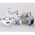
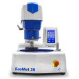
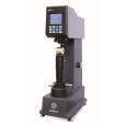
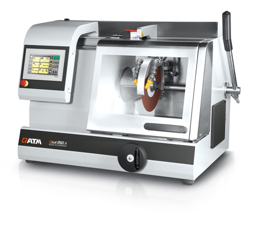
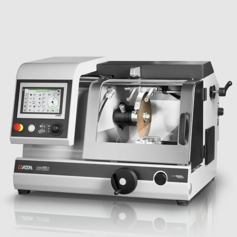
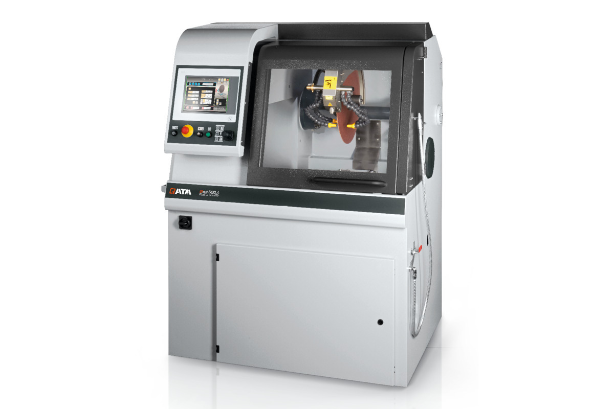
美国标乐为您提供《烧结钢中金相制备分析检测方案(切割机)》,该方案主要用于钢材中理化分析检测,参考标准--,《烧结钢中金相制备分析检测方案(切割机)》用到的仪器有美国标乐 Buehler | IsoMet HS 高速精密切割机、Cast N' Vac 1000 真空镶嵌机、美国标乐 Buehler | EcoMet 30 磨抛机、洛氏硬度计 Rockwell 574 | 美国威尔逊硬度计 Wilson
相关方案
更多
该厂商其他方案
更多