


方案详情
文
Spectroscopic ellipsometry is an ideal technique to characterize film thicknesses and optical constants for photovoltaic applications. Spectroscopic ellipsometers are also sensitive to the presence of rough overlayer and graded optical constants.
The technique provides the advantage to be fast, simple to operate and non-destructive for the characterization of the samples.
方案详情

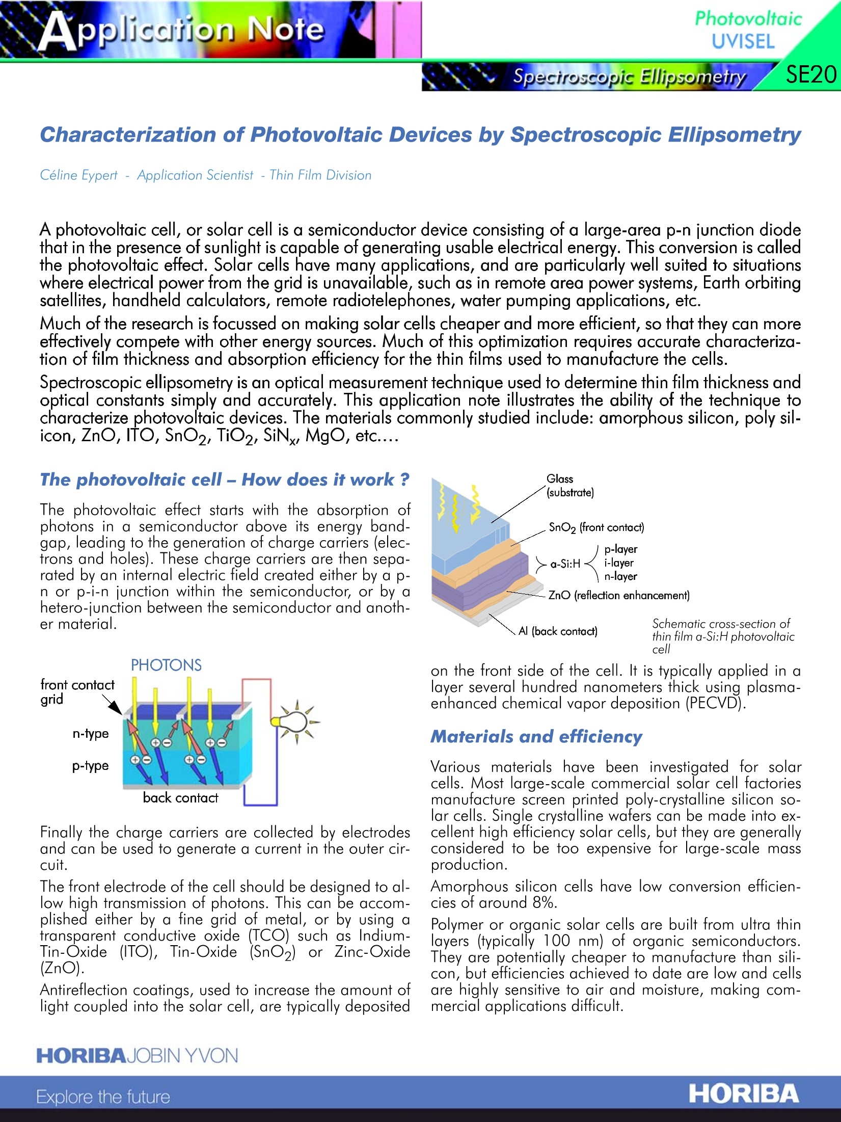
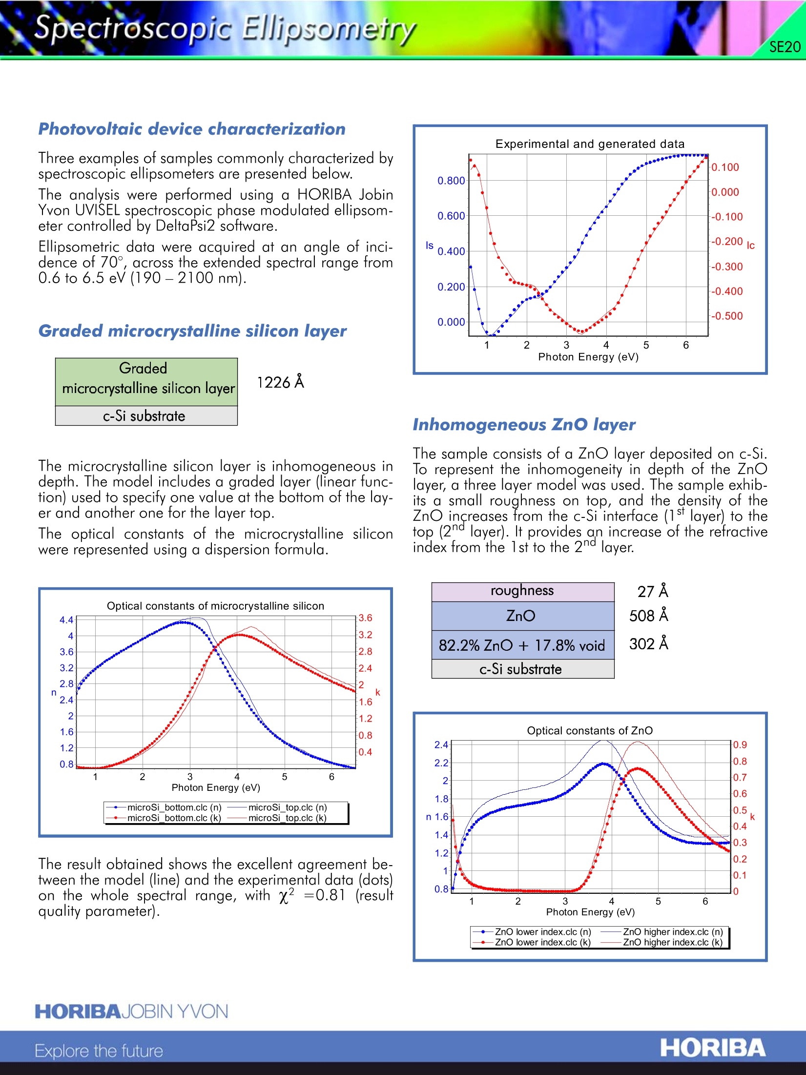
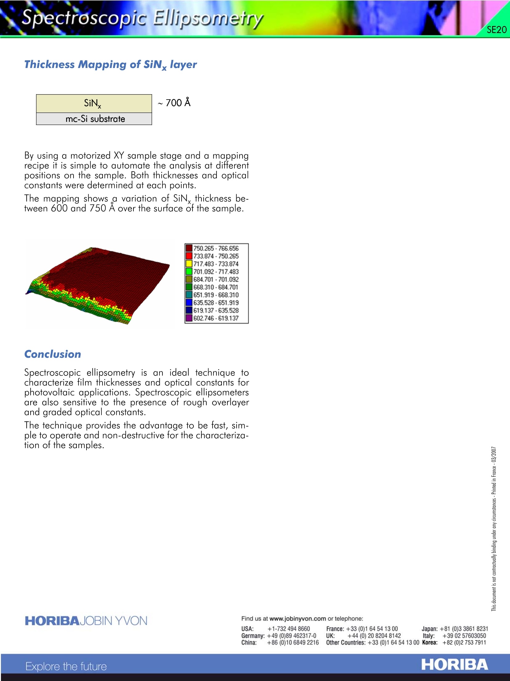
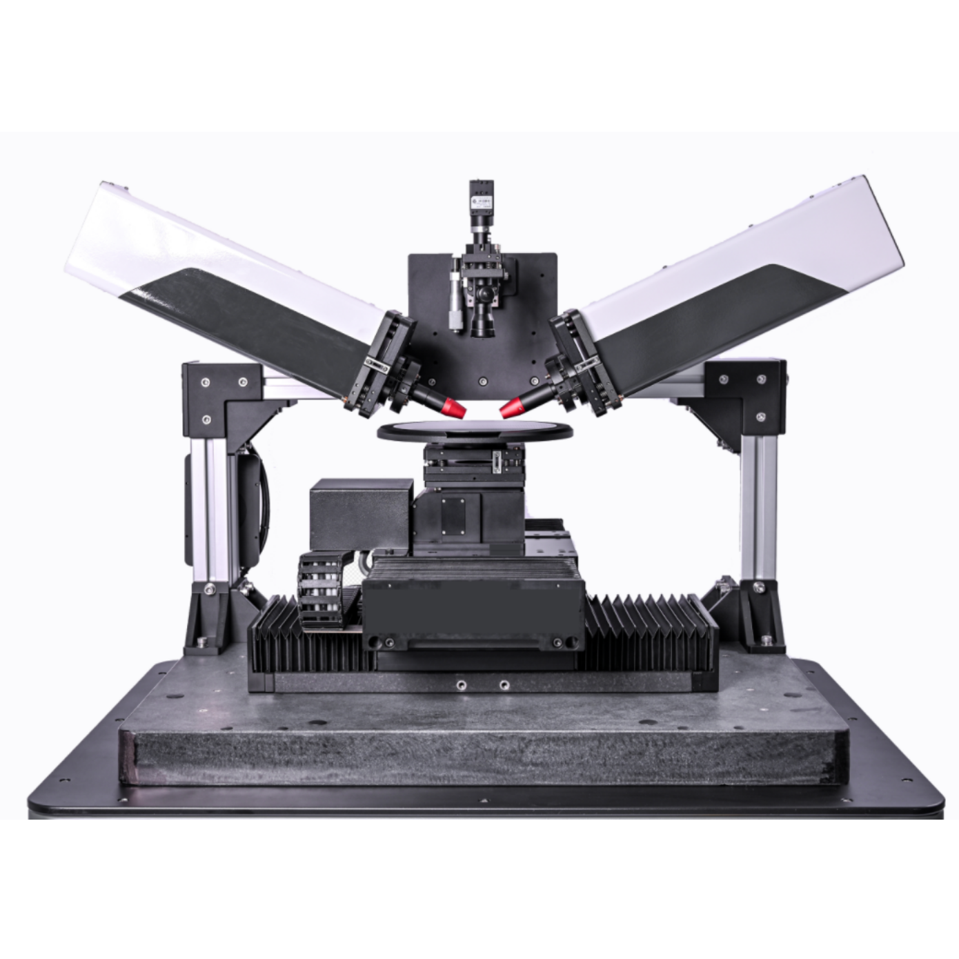
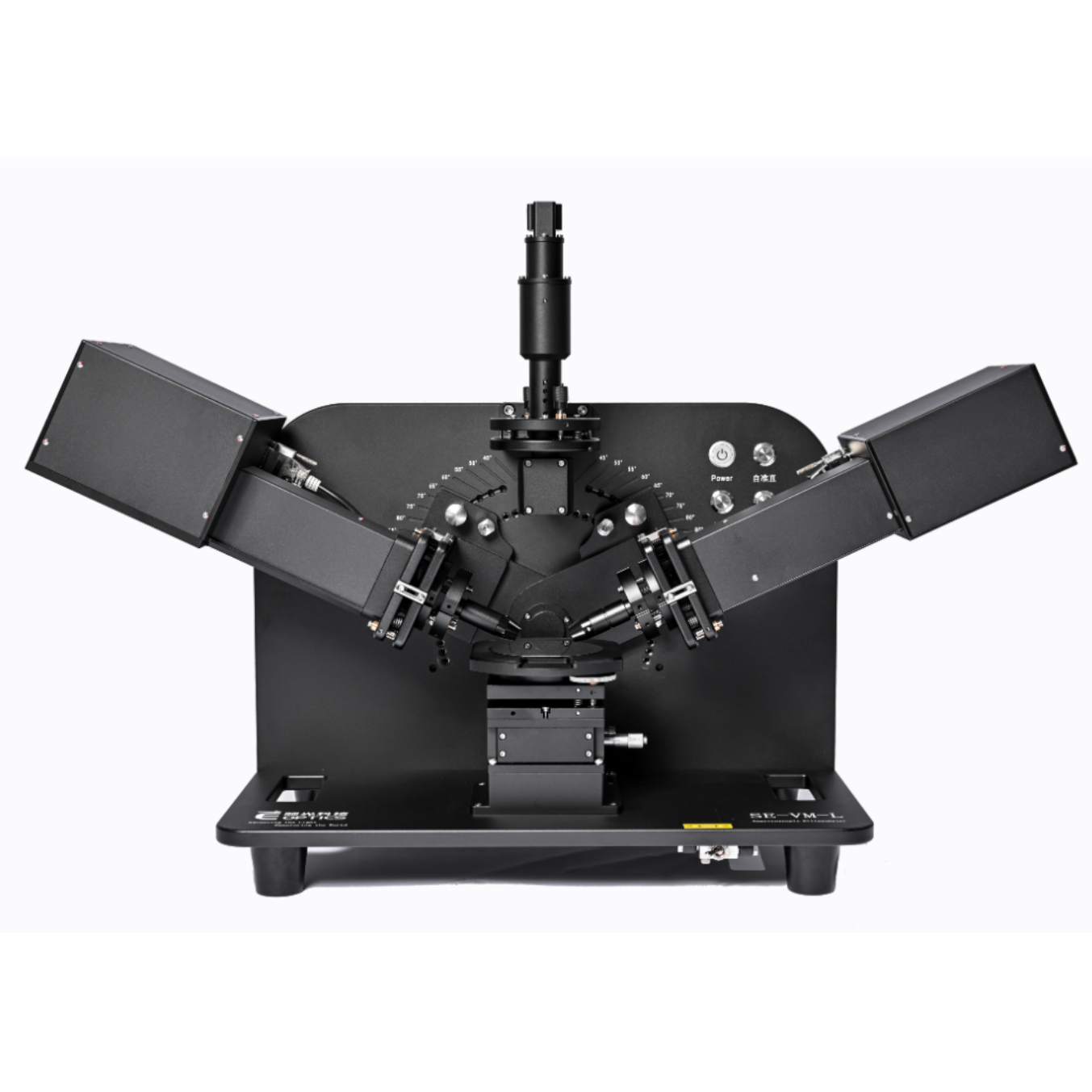
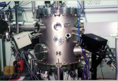
Application NofeSpectroscopic Ellipsometry SE20 Characterization of Photovoltaic Devices by Spectroscopic Ellipsometry Celine Eypert - Application Scientist -Thin Film Division A photovoltaic cell, or solar cell is a semiconductor device consisting of a large-area p-n junction diodethat in the presence of sunlight is capable of generating usable electrical energy. This conversion is calledthe photovoltaic effect. Solar cells have many applications, and are particularly well suited to situationswhere electrical power from the grid is unavailable, such as in remote area power systems, Earth orbitingsatellites, handheld calculators, remote radiotelephones, water pumping applications, etc. Much of the research is focussed on making solarcells cheaper and more efficient, so that they can moreeffectively compete with other energy sources. Much of this optimization requires accurate characteriza-tion of film thickness and absorption efficiency for the thin films used to manufacture the cells. Spectroscopic ellipsometry is an optical measurement technique used to determine thin film thickness andoptical constants simply and accurately. This application note illustrates the ability of the technique tocharacterize photovoltaic devices. The materials commonly studied include: amorphous silicon, poly sil-icon,ZnO,ITO,SnO2, TiO2, SiNw,MgO, etc.... The photovoltaic cell- How does it work ? The photovoltaic effect starts with the absorption ofphotons in a semiconductor above its energy band-gap, leading to the generation of charge carriers (elec-trons and holes). These charge carriers are then sepa-rated by an internal electric field created either by a p-al electricn or p-i-n junction within the semiconductor, or by ahetero-junction between the semiconductor and anoth-er material. tront contact grid Finally the charge carriers are collected by electrodesand can be used to generate a current in the outer cir-cuit. The front electrode of the cell should be designed to al-low high transmission of photons. This can be accom-plished either by a fine grid of metal, or by using atransparent conductive oxide (TCO) such as Indium-Tin-Oxide(ITO),, Tin-Oxide(SnO2))oorr/Zinc-Oxide(ZnO). Antireflection coatings, used to increase the amount oflight coupled into the solar cell, are typically deposited on the front side of the cell. It is typically applied in alayer several hundred nanometers thick using plasma-enhanced chemical vapor deposition (PECVD). Materials and efficiency Various materials have been investigated for solarcells. Most large-scale commercial solar cell factoriesmanufacture screen printed poly-crystalline silicon so-lar cells. Single crystalline wafers can be made into ex-cellent high efficiency solar cells, but they are generallyconsidered to be too expensive for large-scale massproduction. Amorphous silicon cells have low conversion efficien-cies of around 8%. Polymer or organic solar cells are built from ultra thinlayers (typically 100 nm) of organic semiconductors.They are potentially cheaper to manufacture than sili-con, but efficiencies achieved to date are low and cellsare highly sensitive to air and moisture, making com-mercial applications difficult. Photovoltaic device characterization Three examples of samples commonly characterized byspectroscopic ellipsometers are presented below. The analysis were performed using a HORIBA JobinYvon UVISEL spectroscopic phase modulated ellipsom-eter controlled by DeltaPsi2 software. Ellipsometric data were acquired at an angle of inci-dence of 70°, across the extended spectral range from0.6 to 6.5 eV (190-2100 nm). Graded microcrystalline silicon layer c-Si substrate 1226A The microcrystalline silicon layer is inhomogeneous indepth. The model includes a graded layer (linear func-tion) used to specify one value at the bottom of the lay-er and another one for the layer top. The optical constants of the microcrystalline siliconwere represented using a dispersion tormula. The result obtained shows the excellent agreement be-tween the model (line) and the experimental data (dots)on the whole spectral range, with x2=0.81 ((resultquality parameter). Inhomogeneous ZnO layer The sample consists of a ZnO layer deposited on c-Si.To represent the inhomogeneity in depth of the ZnOlayer, a three layer model was used. The sample exhib-its a small roughness on top, and the density of theZnO increases from the c-Si interface (1Slayer) to theop (2nd layer). It provides an increase of the refractiveindex from the 1st to the 2ndlcayer. 27A ZnO 82.2% ZnO + 17.8% void c-Si substrate 508A 302A Thickness Mapping of SiNx layer By using a motorized XY sample stage and a mappingrecipe it is simple to automate the analysis at differentpositions on the sample. Both thicknesses and opticalconstants were determined at each points. The mapping shows a variation of SiN thickness be-tween 600 and 750 A over the surface of the sample. Conclusion Spectroscopic ellipsometry is an ideal technique tocharacterize film thicknesses and optical constants forphotovo tqis gpplicatiens Spectroscopis ellipsometare also sensitive to the presence of rough overlayeiand graded optical constants. The technique provides the advantage to be fast, sim-ple to operate and non-destructive for the characteriza-tion of the samples. USA: +1-732 494 8660France:+33 (0)1 64 54 13 00Japan: +81 (0)3 3861 8231Germany: +49 (0)89 462317-0UK: +44 (0) 20 82048142Italy:+390257603050 China: +86 (0)10 6849 2216 Other Countries: +33 (0)1 64 54 13 00 Korea: +82 (0)2 753 7911 HORIBAExplore the future HORIBAJOBIN YVONHORIBAExplore the future Spectroscopic ellipsometry is an ideal technique to characterize film thicknesses and optical constants for photovoltaic applications. Spectroscopic ellipsometers are also sensitive to the presence of rough overlayer and graded optical constants.The technique provides the advantage to be fast, simple to operate and non-destructive for the characterization of the samples.
确定
还剩1页未读,是否继续阅读?

产品配置单

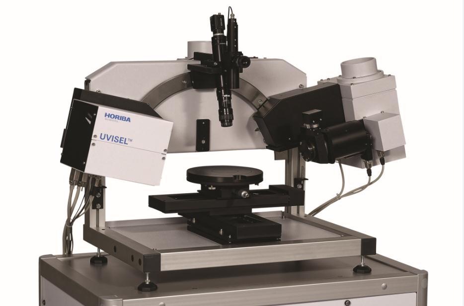
HORIBA(中国)为您提供《光伏器件中厚度,光学常数检测方案(椭偏仪)》,该方案主要用于光电器件中厚度,光学常数检测,参考标准--,《光伏器件中厚度,光学常数检测方案(椭偏仪)》用到的仪器有HORIBA UVISEL Plus研究级经典型椭偏仪
推荐专场
相关方案
更多
该厂商其他方案
更多