


方案详情
文
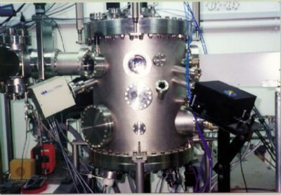
For multilayer structures it is always helpful and often necessary to know the properties of each film. Using the Jobin Yvon UVISEL NIR it is a straightforward procedure to investigate the thickness and optical properties of the complete PDP structure.
方案详情

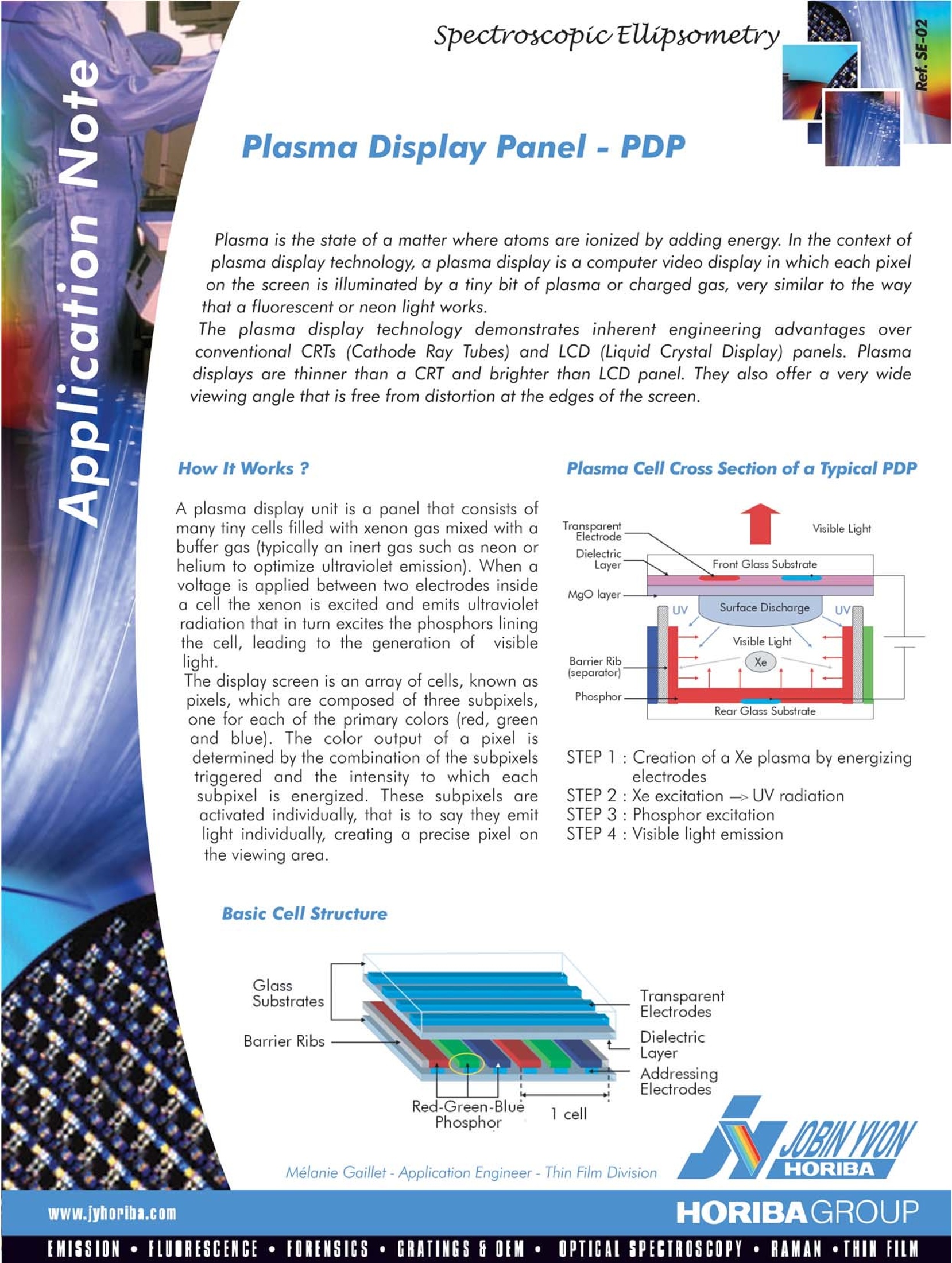
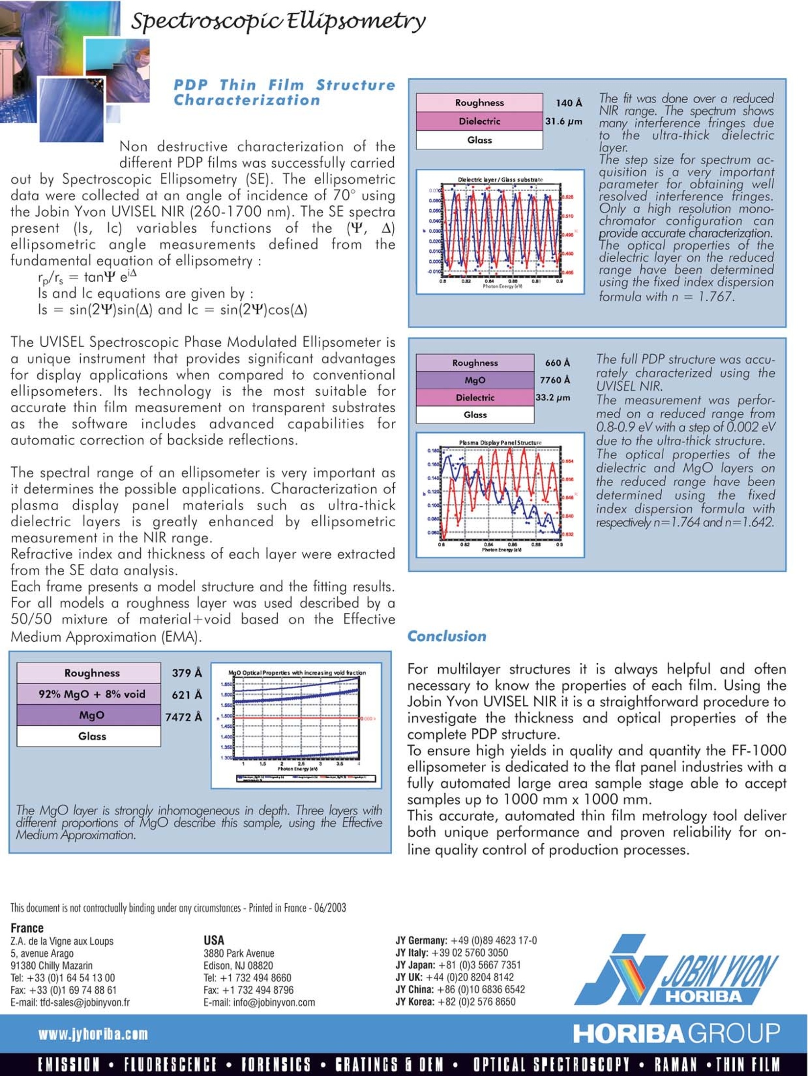
SpectroscopicEUipsometry Plasma Display Panel- PDP Plasma is the state of a matter where atoms are ionized by adding energy. In the context ofplasma display technology, a plasma display is a computer video display in which each pixelon the screen is illuminated by a tiny bit of plasma or charged gas, very similar to the waythat a fluorescent or neon light works. The plasma display technology demonstrates inherent engineering advantages overconventional CRTs (Cathode Ray Tubes) and LCD (Liquid Crystal Display) panels. Plasmadisplays are thinner than a CRT and brighter than LCD panel. They also offer a very wideviewing angle that is free from distortion at the edges of the screen. A plasma display unit is a panel that consists ofmany tiny cells filled with xenon gas mixed with abuffer gas (typically an inert gas such as neon orhelium to optimize ultraviolet emission). When avoltage is applied between two electrodes insidea cell the xenon is excited and emits ultravioletradiation that in turn excites the phosphors liningthe cell, leading to the generation oft yvisiblelight. The display screen is an array of cells, known aspixels, which are composed of three subpixels,one for each of the primary colors (red, greenand blue). The color output of a pixel isdetermined by the combination of the subpixelstriggered and the intensity to which eachsubpixel is energized. These subpixels careactivated individually, that is to say they emitlight individually, creating a precise pixel onthe viewing area. Plasma Cell Cross Section of a Typical PDP STEP 1: Creation of a Xe plasma by energizingelectrodes STEP 2 : Xe excitation ->UV radiation STEP 3 : Phosphor excitation STEP 4 : Visible light emission PDP Thin Film StructureCharacterization Non destructive characterization of thedifferent PDP films was successfully carriedout by Spectroscopic Ellipsometry (SE). The ellipsometricdata were collected at an angle of incidence of 70° usingthe Jobin Yvon UVISEL NIR (260-1700 nm). The SE spectrapresent(ls, lc) variablesSffunctions of the (, A)ellipsometric angle measurementss cdefined from thefundamental equation of ellipsometry : rp/rs = tanY e ls and lc equations are given by: Is= sin(2)sin(A) and lc = sin(2Y)cos(A) The UVISEL Spectroscopic Phase Modulated Ellipsometer isa unique instrument that provides significant advantagesfor display applications when compared to conventionalellipsometers. Its technology is the most suitable foraccurate thin film measurement on transparent substratesas, thesoftware includes advanced capabilitie:fforautomatic correction of backside reflections. The spectral range of an ellipsometer is very important asit determines the possible applications. Characterization ofplasma displayy ppanel materialssuchn as ultra-thickdielectric layerss is; greatly enhanced by ellipsometricmeasurement in the NIR range. Refractive index and thickness of each layer were extractedfrom the SE data analysis. Each frame presents a model structure and the fitting results.For all models a roughness layer was used described by a50/50 mixture of material+void based on the EffectiveMedium Approximation (EMA). Roughness 92% MgO+ 8%void MgO Glass Roughness 140A Dielectric 31.6 pm Glass The fit was done over a reducedNIR range. The spectrum showsmany interference fringes dueto ttheultra-thick dielectriclayer. The step size for spectrum ac-quisition is a very importantparameter for obtaining wellresolved interference fringes.Only a high resolution monochromator configuration canprovide accurate characterization.The optical properties of thedielectric layer on the reducedrange have been determinedusing the fixed index dispersionformula with n= 1.767. Roughness 660A The full PDP structure was accu- 7760 A rately characterized using the MgO UVISEL NIR. Dielectric 33.2 pm The measurement was perfor- Glass med on a reduced range from 0.8-0.9 eV with a step of 0.002 eV due to the ultra-thick structure. The optical properties of thedielectric and MgO layers onthe reduced range have beendetermined using the fixedindex dispersion formula withrespeclivelyn=1.764 andn=1.642. Conclusion For multilayer structures it is always helpful and oftennecessary to know the properties of each film. Using theJobin Yvon UVISEL NIR it is a straightforward procedure toTOinvestigate the thickness and optical properties of thecomplete PDP structure. To ensure high yields in quality and quantity the FF-1000ellipsometer is dedicated to the flat panel industries with afully automated large area sample stage able to acceptsamples up to 1000 mmx1000 mm. This accurate, automated thin film metrology tool deliverboth unique performance and proven reliability for on-line quality control of production processes. Z.A. de la Vigne aux LoupsUSAJY Germany:+49 (0)89 4623 17-05,avenue Arago3880 Park AvenueJY Italy:+39 02 5760305091380 Chilly MazarinEdison, NJ 08820JY Japan: +81 (0)3 5667 7351Tel:+33 (0)1 64 5413 00Tel: +1 732 494 8660JY UK: +44 (0)20 8204 8142Fax: +33 (0)1 69 74 88 61Fax: +1 732 494 8796JY China: +86i (0)10 6836 6542E-mail: tfd-sales@jobinyvon.frE-mail: info@jobinyvon.comJY Korea: +82 (0)2 576 8650 HORIBAGROUP EMISSION·FLUORESCENCE·FORENSICS·CRATINGS F OEM· OPTICAL SPECTROSCOPY·RAMAN ·THIN FILM For multilayer structures it is always helpful and often necessary to know the properties of each film. Using the Jobin Yvon UVISEL NIR it is a straightforward procedure to investigate the thickness and optical properties of the complete PDP structure.
确定
还剩1页未读,是否继续阅读?

产品配置单

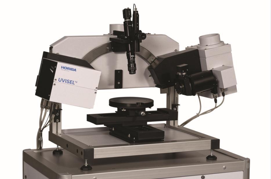
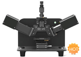
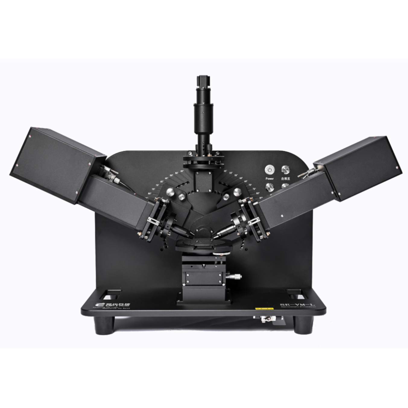
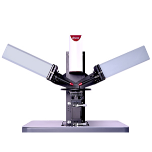
HORIBA(中国)为您提供《PDP等离子体显示屏中厚度,光学常数检测方案(椭偏仪)》,该方案主要用于其他中厚度,光学常数检测,参考标准--,《PDP等离子体显示屏中厚度,光学常数检测方案(椭偏仪)》用到的仪器有HORIBA UVISEL Plus研究级经典型椭偏仪
推荐专场
相关方案
更多
该厂商其他方案
更多