


布鲁克独有的PeakForce SECM™ 模块是全球首创的完备商用解决方案,在基于原子力显微镜的扫描电化学显微镜上实现了小于100纳米的空间分辨率。
方案详情

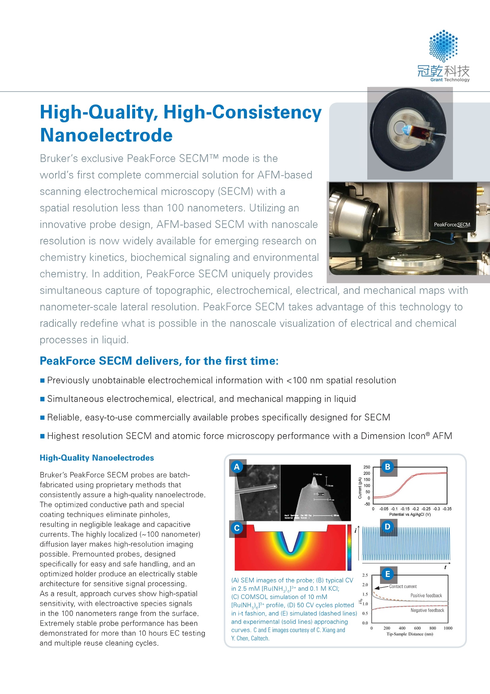
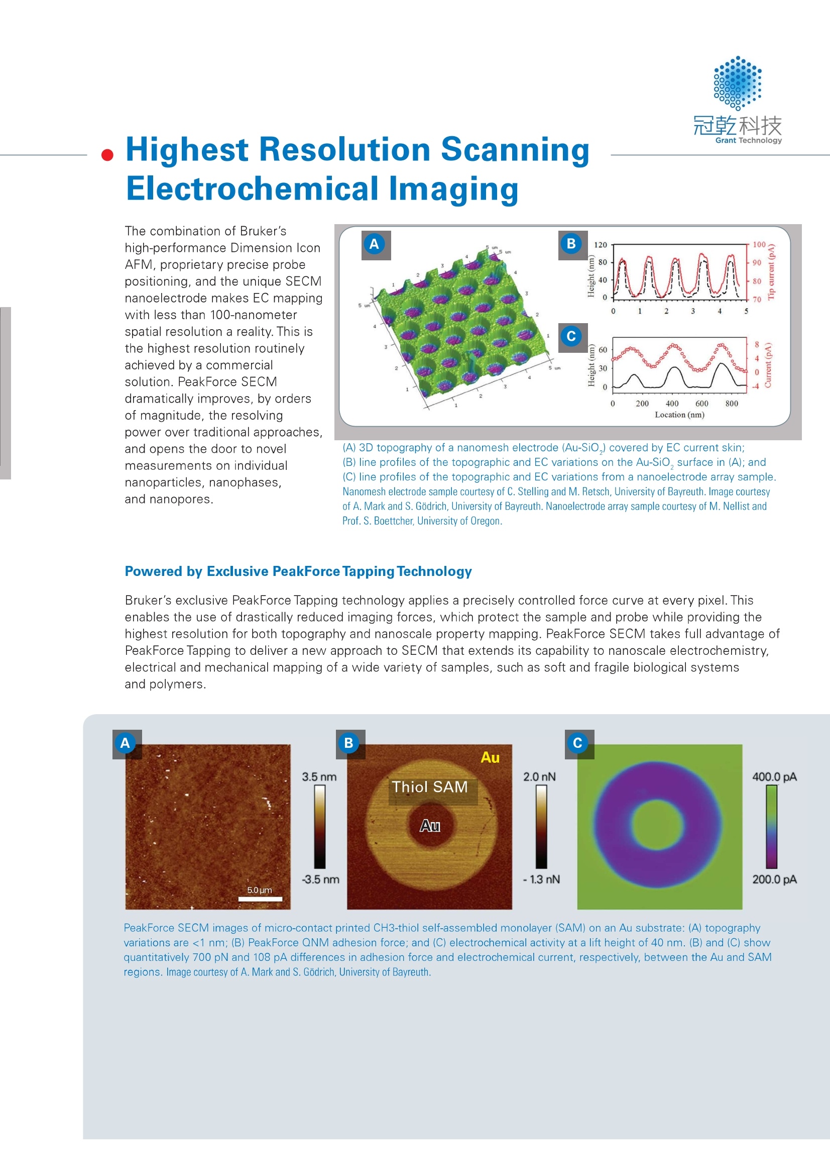
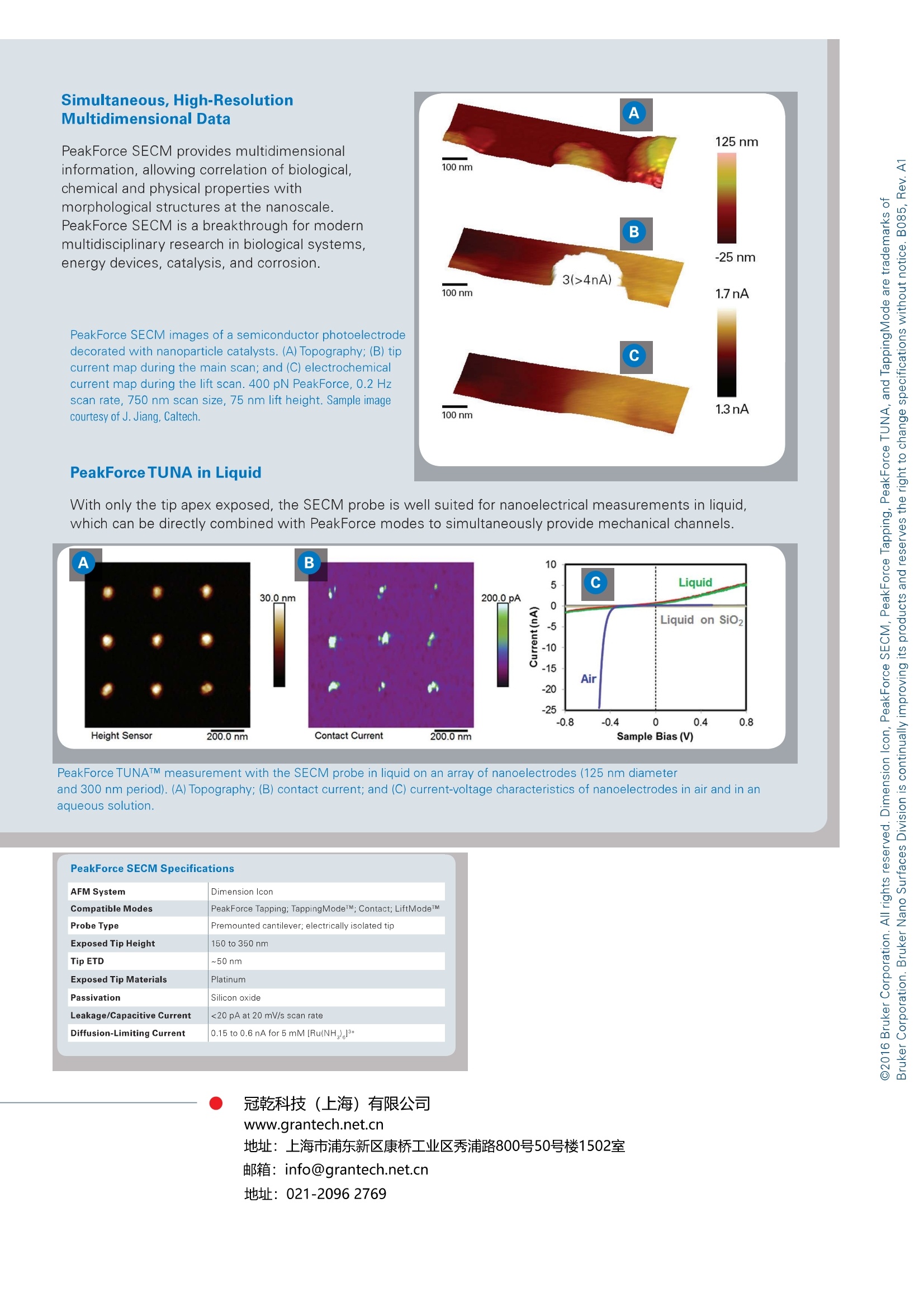
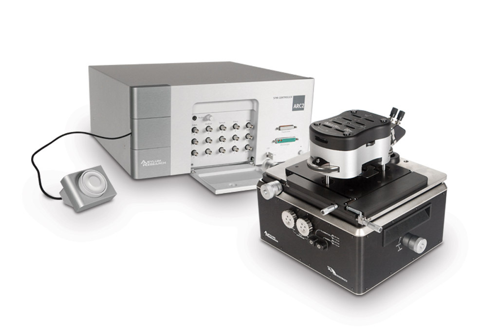
地址:上海市浦东新区康桥工业区秀浦路800号50号楼1502室 PeakForce SECM AFM-Based Scanning Electrochemical Microscopy and In Situ Electrical Mapping in Liquid Innovation with Integrity world's first complete commercial solution for AFM-basedscanning electrochemical microscopy (SECM) with aspatial resolution less than 100 nanometers.Utilizing aninnovative probe design, AFM-based SECM with nanoscaleresolution is now widely available for emerging research onchemistry kinetics, biochemical signaling and environmentalchemistry. In addition, PeakForce SECM uniquely provides simultaneous capture of topographic, electrochemical, electrical, and mechanical maps withnanometer-scale lateral resolution. PeakForce SECM takes advantage of this technology toradically redefine what is possible in the nanoscale visualization of electrical and chemicalprocesses in liquid. PeakForce SECM delivers, for the first time: Previously unobtainable electrochemical information with <100 nm spatial resolution iSimultaneous electrochemical, electrical, and mechanical mapping in liquidiReliable, easy-to-use commercially available probes specifically designed for SECM i Highest resolution SECM and atomic force microscopy performance with a Dimension Icon@ AFM High-Quality Nanoelectrodes Bruker's PeakForce SECM probes are batch-fabricated using proprietary methods thatconsistently assure a high-quality nanoelectrode.The optimized conductive path and specialcoating techniques eliminate pinholes,resulting in negligible leakage and capacitivecurrents. The highly localized (~100 nanometer)diffusion layer makes high-resolution imagingpossible. Premounted probes, designedspecifically for easy and safe handling, and anoptimized holder produce an electrically stablearchitecture for sensitive signal processing.As a result, approach curves show high-spatialsensitivity, with electroactive species signalsin the 100 nanometers range from the surface.Extremely stable probe performance has beendemonstrated for more than 10 hours EC testingand multiple reuse cleaning cycles. The combination of Bruker'shigh-performance Dimension IconAFM, proprietary precise probepositioning, and the unique SECMnanoelectrode makes EC mappingwith less than 100-nanometerspatial resolution a reality. This isthe highest resolution routinelyachieved by a commercialsolution. PeakForce SECMdramatically improves, by ordersof magnitude, the resolvingpower over traditional approaches,and opens the door to novelmeasurements on individualnanoparticles, nanophases,and nanopores. (A) 3D topography of a nanomesh electrode (Au-SiO,) covered by EC current skin;(B) line profiles of the topographic and EC variations on the Au-SiO, surface in (A); and(C) line profiles of the topographic and EC variations from a nanoelectrode array sample.Nanomesh electrode sample courtesy of C. Stelling and M. Retsch, University of Bayreuth. Image courtesyof A. Mark and S. Godrich, University of Bayreuth. Nanoelectrode array sample courtesy of M. Nellist andProf. S. Boettcher, University of Oregon. Powered by Exclusive PeakForce Tapping Technology Bruker’s exclusive PeakForce Tapping technology applies a precisely controlled force curve at every pixel. Thisenables the use of drastically reduced imaging forces, which protect the sample and probe while providing thehighest resolution for both topography and nanoscale property mapping. PeakForce SECM takes full advantage ofPeakForce Tapping to deliver a new approach to SECM that extends its capability to nanoscale electrochemistry,electrical and mechanical mapping of a wide variety of samples, such as soft and fragile biological systemsand polymers. PeakForce SECM images of micro-contact printed CH3-thiol self-assembled monolayer (SAM) on an Au substrate: (A) topographyvariations are <1 nm; (B) PeakForce QNM adhesion force; and (C) electrochemical activity at a lift height of 40 nm. (B) and (C) showquantitatively 700 pN and 108 pA differences in adhesion force and electrochemical current, respectively, between the Au and SAMregions. Image courtesy of A. Mark and S. Godrich, University of Bayreuth. Simultaneous, High-ResolutionMultidimensional Data PeakForce SECM provides multidimensionalinformation, allowing correlation of biological,chemical and physical properties withmorphological structures at the nanoscale.PeakForce SECM is a breakthrough for modernmultidisciplinary research in biological systems,energy devices, catalysis, and corrosion. PeakForce SECM images of a semiconductor photoelectrodedecorated with nanoparticle catalysts. (A) Topography;(B) tipcurrent map during the main scan; and (C) electrochemicalcurrent map during the lift scan. 400 pN PeakForce, 0.2 Hzscan rate, 750 nm scan size, 75 nm lift height. Sample imagecourtesy of J. Jiang, Caltech. PeakForce TUNA in Liquid With only the tip apex exposed, the SECM probe is well suited for nanoelectrical measurements in liquid,which can be directly combined with PeakForce modes to simultaneously provide mechanical channels. PeakForce TUNATM measurement with the SECM probe in liquid on an array of nanoelectrodes (125 nm diameterand 300 nm period). (A) Topography; (B) contact current; and (C) current-voltage characteristics of nanoelectrodes in air and in anaqueous solution. AFM System Dimension Icon Compatible Modes PeakForce Tapping; TappingModeTM; Contact; LiftModeTM Probe Type Premounted cantilever; electrically isolated tip Exposed Tip Height 150 to 350 nm Tip ETD ~50 nm Exposed Tip Materials Platinum Passivation Silicon oxide Leakage/Capacitive Current <20 pA at 20mV/s scan rate Diffusion-Limiting Current 0.15 to 0.6 nA for 5 mM [Ru(NH,)1+ 冠乾科技(上海)有限公司www.grantech.net.cn 邮箱: info@grantech.net.cn 地址:021-20962769 完整的SECM电化学显微镜解决方案 布鲁克独有的PeakForce SECM™ 模块是全球首创的完备商用解决方案,在基于原子力显微镜的扫描电化学显微镜上实现了小于100纳米的空间分辨率。通过创新性探针设计,可实现纳米级分辨率的基于原子力显微镜的扫描电化学显微镜目前已广泛应用于新兴研究领域,如化学动力学,生物化学信号传导和环境化学等。此外,此技术可以纳米级横向分辨同时获取形貌、电化学、电学和机械性能等图谱。PeakForce SECM™充分利用峰值力模式的优势从根本上重新定义了在液下能实现哪些电学和化学过程的纳米尺度的观察。 PeakForce SECM首次实现了:(1)以往无法获得的<100 nm 空间分辨率的电化学信息(2)同时实现液相下电化学、电学和机械性能等图谱(3)专为SECM设计的可靠而简单易用的商用原子力探针(4)在Dimension Icon®原子力显微镜上实现最高分辨的SECM和原子力显微成像Au上的一个甜甜圈型图案,使用PeakForce SECM在微压印SAM(自组装)样品上成像。(A) 形貌图中高度差仅几个纳米;(B) 黏附力图清晰地显示出两种化学性质不同的区域; (C) 电流图显示出SAM因其绝缘特性降低了针尖的法拉第电流。 Image courtesy of A. Mark and S. G?drich, University of Bayreuth.
确定
还剩2页未读,是否继续阅读?

产品配置单
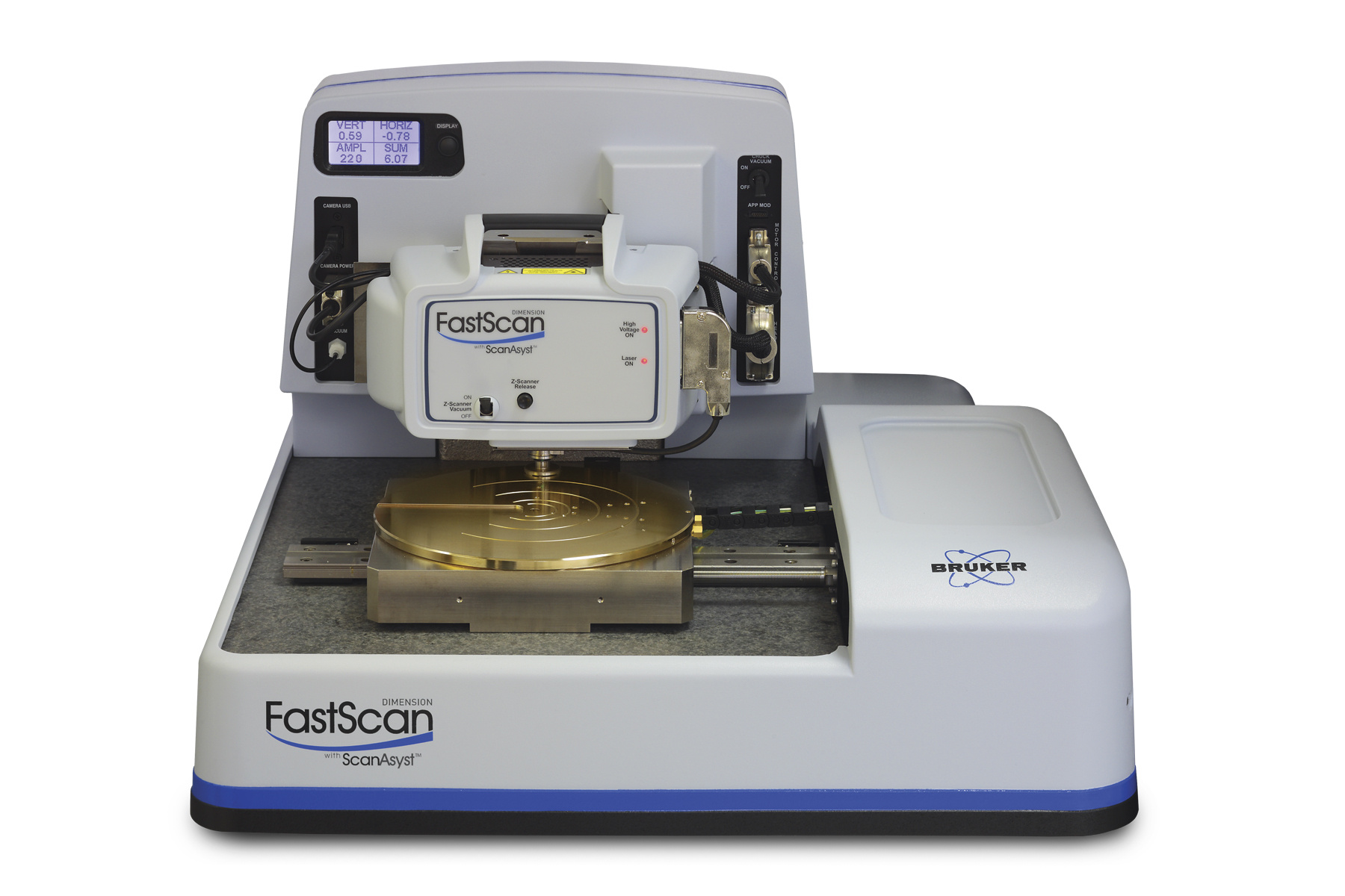
冠乾科技(上海)有限公司为您提供《化学/生物中电化学性能检测方案(扫描探针)》,该方案主要用于其他中电化学性能检测,参考标准--,《化学/生物中电化学性能检测方案(扫描探针)》用到的仪器有布鲁克Dimension FastScan原子力显微镜
推荐专场
相关方案
更多