


方案详情
文
Above image is a copper sample coated with nickel and gold. Since nickel and copper have similar atomic number, it is hard to differentiate the boundary between the two. Through chemical etching, as shown in the right image, two layers can be easily distinguished. If etching is impossible, layers can be distinguished in the BSE mode.
方案详情

WINDOW FOR NANO WORLD with COXEM WWw.coxem.com Overview SEM can be used to assess topography of metals and related coatings. BSE mode is extremely useful in this case. Metal with Chemical Etching Above image is a copper sample coated with nickel and gold.Since nickel and copper have similar atomic number, it ishard to differentiate the boundary between the two. Throughchemical etching, as shown in the right image, two layers canbe easily distinguished. If etching is impossible, layers can bedistinguished in the BSE mode. Metal Surface Metal objects require little special sample preparation forSEM imaging. Coating is not necessary since they are highlyconductive. If the surface level is similar, particles may not bedistinguished clearly. To account for this, the BSE mode can beutilized. The BSE mode detects atomic number differences onand below the surface, so high atomic number particles can beeasily differentiated. Back Scattered Electrons (BSE) BSE detector can be easily integrated into COXEM’s SEM. BSEimaging is as generally useful as SE imaging, especially whengathering composition and topography features of images withhigh atomic number contrast. For example, when viewingbiological samples stained or coated with heavy metals, the BSEmode can be used to detect metals more pronouncedly thanthe SE mode. BSE image can be acquired at both high and lowvacuum. Poly Wire The sample is a poly wire partially coated with copper andcarbon. When the image is taken at high voltage, carbon coatingcannot be viewed due to carbon's low atomic number. Toaccount for this, accelerating voltage is lowered to see additionalinformation on the surface. At low voltage, carbon is easilyviewed, as illustrated in the left image. High Voltage .W k 15-03-1 X1,000, 30kV Metals Above image is a copper sample coated with nickel and gold. Since nickel and copper have similar atomic number, it is hard to differentiate the boundary between the two. Through chemical etching, as shown in the right image, two layers can be easily distinguished. If etching is impossible, layers can be distinguished in the BSE mode.
确定


还剩1页未读,是否继续阅读?

产品配置单

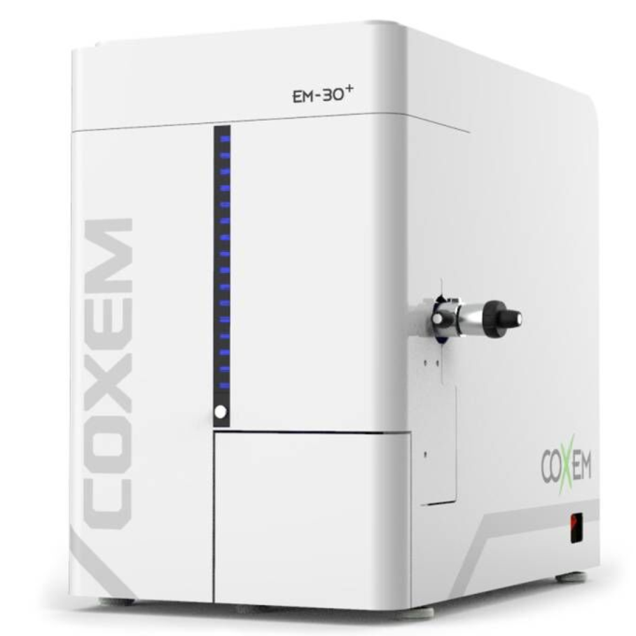
北京天耀科技有限公司为您提供《金属材料中形态分析检测方案(扫描电镜)》,该方案主要用于其他中形态分析检测,参考标准--,《金属材料中形态分析检测方案(扫描电镜)》用到的仪器有库赛姆(COXEM)EM-30+ 台式扫描电镜
推荐专场


相关方案
更多