


方案详情
文
The Controlled Pattern Growth of Aligned Carbon Nanotubes
Abstract
Micropatterns of aligned carbon nanotubes (CNTs) have been prepared by chemical vapor deposition (CVD) method, and patterned structure of aligned CNTs was controlled through patterned formation of silicon oxide (SiO2) using lithographic technology. The simultaneous growth of carbon nanotubes in different directions could be realized. The building of nanotube-based micro-pattern is useful for fabricating electrical devices.
(请下载全文欣赏)
方案详情

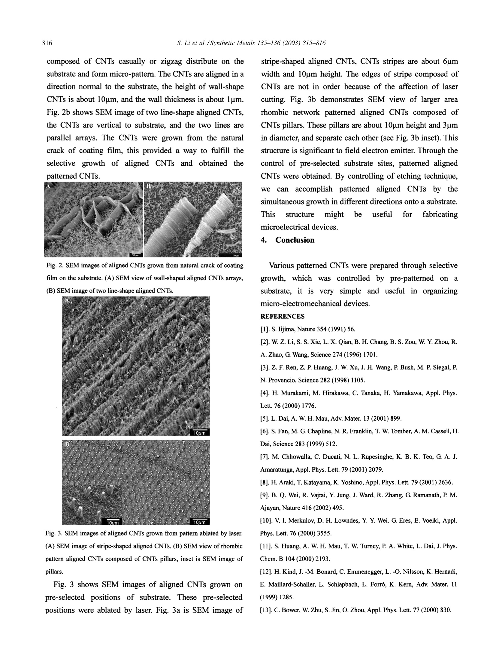
SYNTHETICMETALSSynthetic Metals 135-136 (2003)815-816www.elsevier.com/locate/synmet S. Li et al./Synthetic Metals 135-136 (2003)815-816816 The Controlled Pattern Growth of Aligned Carbon Nanotubes Shuhong Li, Huan Liu, Huafeng Li, Jin Zhai, Lei Jiang*, Daoben Zhu Center ofMolecular Science, Institute of Chemistry, CAS, Beijing 100080,China Abstract Micropatterns of aligned carbon nanotubes (CNTs) have been prepared by chemical vapor deposition (CVD) method, and patternedstructure of aligned CNTs was controlled through patterned formation of silicon oxide (SiOz) using lithographic technology. Thesimultaneous growth of carbon nanotubes in different directions could be realized. The building of nanotube-based micro-pattern is usefulfor fabricating electrical devices. Keywords: graphite and related compounds, manipulation of surface structure and morphology Carbon nanotubes (CNTs) have attracted a great deal ofresearch interests because of their superior mechanical,electrical, and other properties combined with chemicalstability since their discovery by Iijima in 1991. 1-5 AlignedCNTs and patterned aligned CNTs are very important tomany applications such as electron emitter devices. [6-8] Thecontrolled growth of micro-patterned and/or aligned CNTshas been realized by a few methods. 16-13] For example, byusing CVD method and soft-lithographic techniquespatterned aligned CNTs were generated on the substrates.[11,12] But there has been a challenge to control the patternedaligned CNTs growth. In this paper, we applied an approachto control patterned growth of aligned CNTs throughselective growth of the nanotubes on a substrate bypyrolysis of Iron (II) phthalocyanine (FePc). 2. Experimental section Silicon oxide plate or quartz plate partially coated byinorganic oxide or metal thin film was used as substrate.Inorganic oxide film was coated on the substrate byspin-coating or dip-coating, metal thin film was coated bymagnetic sputtering. The laser was used to ablate definiteregion of coating films in order to get various patterns onthe substrate, such as stripe-shape, separated dots. Thesubstrate was then loaded on a quartz tube in the CVD ( * Corresponding Author: Tel & Fax: 0086-10-82627566; ) reactor. Ar/H (1:1 v/v) was flowed into the CVD reactorwhile raising and lowering the temperature. CNTs weregrown at region of 900℃ while FePc was placed where thetemperature was about 550-560℃. CNTs were deposited inthe definite positions of substrate for several minutes. Thepatterns and the structure morphology of selective growthof aligned CNTs were examined by a scanning electronmicroscope (SEM) (JSM6700F, Japan). The schematicprocess of fabricating patterned CNTs is demonstrated inFigure 1. Fig. 1. The schematic illustration fabricating patterned carbon nanotubes 3.Result and discussion Fig. 2 shows SEM images of aligned CNTs deposited onthe substrate, aligned CNTs were grown vertically out fromthe coating film-free region, The selective growth of CNTsgenerated patterned micro-structure aligned CNTs. Thelength of CNTs increased with CVD growth time. Fig. 2a isSEMimage of thewall-shaped CNTs.The "walls" ( 0379-6779/03/$- s ee fr o nt matter C 2 0 0 3 Elsevier Science B.V. All righ t s res e rved.doi:10.1016/S0379-6779(02)00908-6 ) composed of CNTs casually or zigzag distribute on thesubstrate and form micro-pattern. The CNTs are aligned in adirection normal to the substrate, the height of wall-shapeCNTs is about 10um, and the wall thickness is about 1pm.Fig. 2b shows SEM image of two line-shape aligned CNTs,the CNTs are vertical to substrate, and the two lines areparallel arrays. The CNTs were grown from the naturalcrack of coating film, this provided a way to fulfill theselective growth of aligned CNTsand obtainedl thepatterned CNTs. Fig. 2. SEM images of aligned CNTs grown from natural crack of coatingfilm on the substrate. (A) SEM view of wall-shaped aligned CNTs arrays,(B) SEM image of two line-shape aligned CNTs. 10pm Fig. 3. SEM images of aligned CNTs grown from pattern ablated by laser. (A) SEM image of stripe-shaped aligned CNTs. (B) SEM view of rhombicpattern aligned CNTs composed of CNTs pillars, inset is SEM image ofpillars. Fig. 3 shows SEM images of aligned CNTs grown onpre-selected positions of substrate.These pre-selectedpositions were ablated by laser. Fig. 3a is SEM image of stripe-shaped aligned CNTs, CNTs stripes are about 6pmwidth and 10um height. The edges of stripe composed ofCNTs are not in order because of the affection of lasercutting. Fig. 3b demonstrates SEM view of larger arearhombic network patterned aligned CNTs composed ofCNTs pillars. These pillars are about 10um height and 3umin diameter, and separate each other (see Fig. 3b inset). Thisstructure is significant to field electron emitter. Through thecontrol of pre-selected substrate sites, patterned alignedCNTs were obtained. By controlling of etching technique,we canaccomplish patterned aligned CNTssbby thesimultaneous growth in different directions onto a substrate.This structurenmight be useful for fabricatingmicroelectrical devices. 4. Conclusion Various patterned CNTs were prepared through selectivegrowth, whichwas controlled by pre-patterned on asubstrate, it isvery simple and useful in organizingmicro-electromechanical devices. ( REFERENCES ) ( [1]. S. Iijima, Nature 354 (1991) 56. ) ( [2]. W. Z. Li, S. S. Xie, L. X. Qian, B. H. Chang, B. S. Zou, W. Y. Zhou, R.A. Zhao, G.Wang, S c ience 274 (1996) 1701. ) ( [3]. Z. F. Ren, Z. P . Huang, J. W. Xu, J. H. Wa n g, P. Bush, M. P. Si e gal, P.N. Provencio,Science 282 (1998) 1 1 05. ) ( [4]. H. Murakami,M. Hirakawa, C. T anaka, H . Yamakawa, Appl. P hys.Lett. 76 (2000) 1776. ) ( [5]. L.Dai, A. W. H. Mau, Adv. M ater. 1 3 (2001) 899. ) ( [6]. S. Fan, M.G. Chapline, N. R. Franklin, T. W . To m ber, A. M. C assell, H.Dai, Science 283 (1999) 512. ) ( [7]. M. Chhowalla, C. Ducati, N. L . Rupesinghe, K. B. K. Te o , G. A. J.Amaratunga, Appl. Phys. Lett. 79 (2001) 2079. ) ( [8]. H. Araki, T. Katayama, K. Yoshino, Appl. Phys. Lett. 79(2001) 2636. ) ( [9]. B. Q. Wei, R. Vajtai, Y. Jung, J. Ward, R. Zhang, G. Ramanath, P. M . Ajayan, Nature 416 (2002) 495. ) ( [ 1 0]. V . I . Merkulov,D . H . Lowndes, Y. Y. We i . G. Er e s, E. Voelkl, A p pl.Phys. Lett. 76 (2000) 3555. ) ( [11]. S. Huang, A. W. H. Mau, T. W. Turney, P. A. Wh i te,L. Dai , J. P hys.Chem. B 104 (2000)2193. ) ( [12]. H. Kind, J.-M. Bonard, C . E mmenegger, L. - O. Nilsson, K. He r nadi,E. M aillard-Schaller, L. Schlapbach, L . F orr6, K . Kern, A d v. Mater. 11(1999) 1285. ) ( [ 13]. C. B ower, W . Zhu, S. Ji n , O. Zhou, Appl. Phy s . Let t . 77 (20 0 0)830. )
确定

还剩1页未读,是否继续阅读?

北京东方德菲仪器有限公司为您提供《中国客户在国际刊物上发表的应用文章:阵列碳纳米管的可控生长》,该方案主要用于碳材料中--检测,参考标准--,《中国客户在国际刊物上发表的应用文章:阵列碳纳米管的可控生长》用到的仪器有
相关方案
更多