


方案详情
文
安捷伦的纳米压痕仪是压痕仪的国家行业标准,具有最高的精度和稳定性,用户数量最多。
安捷伦的纳米压痕仪是压痕仪的国家行业标准,具有最高的精度和稳定性,用户数量最多。
方案详情

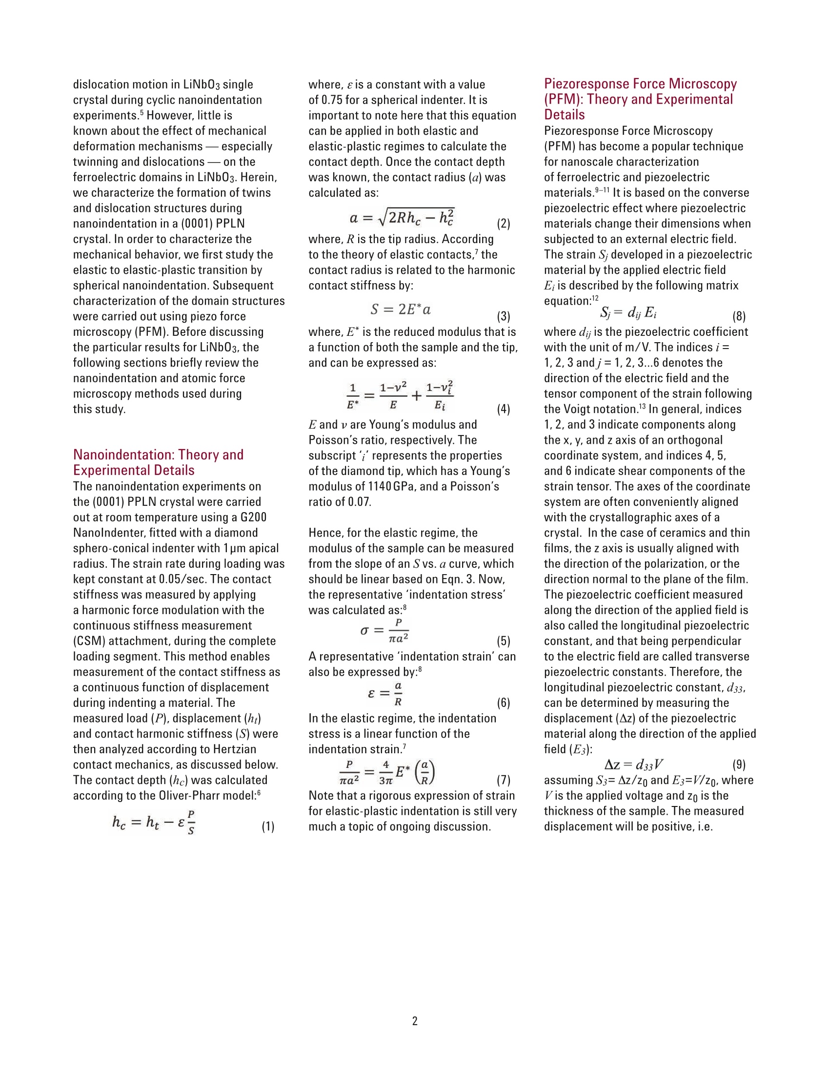
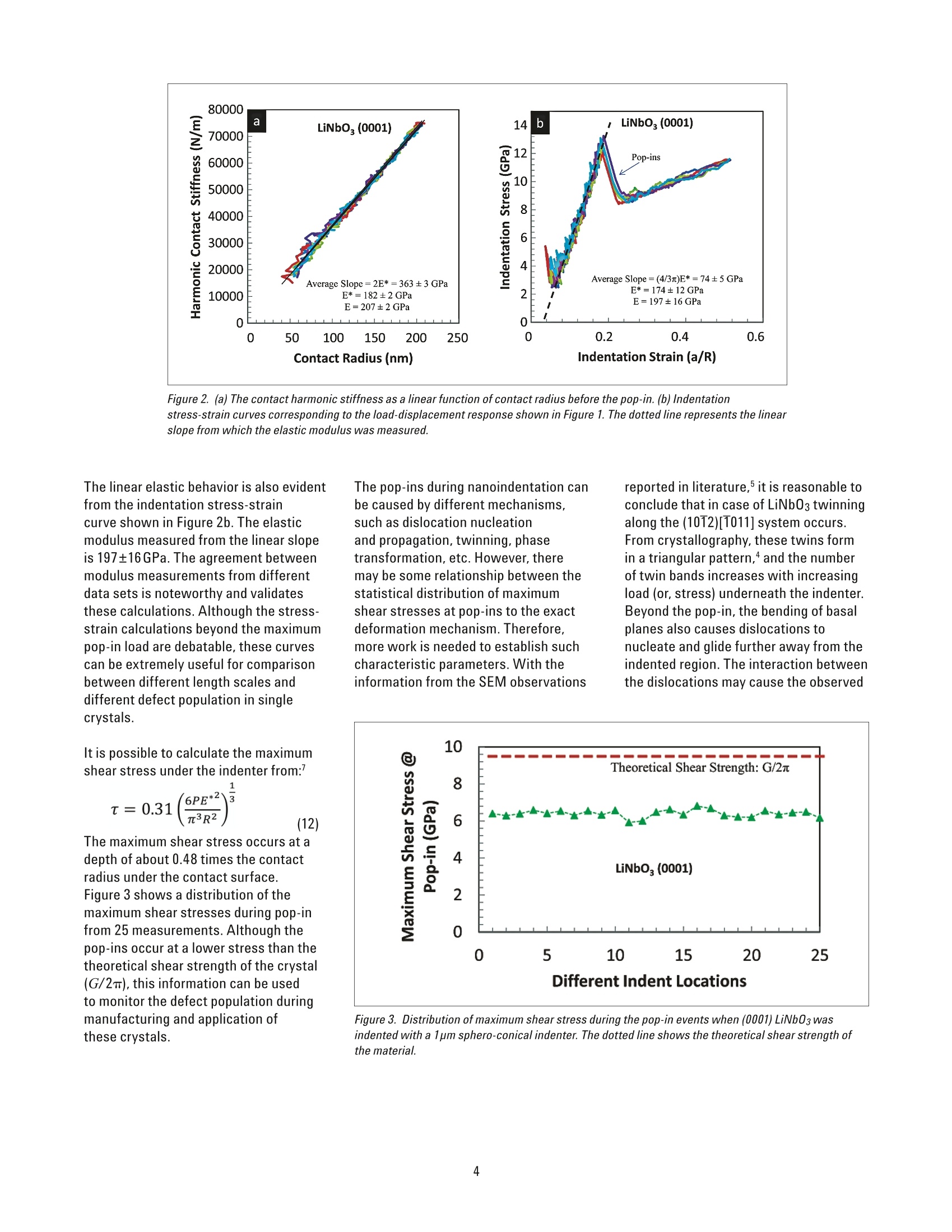
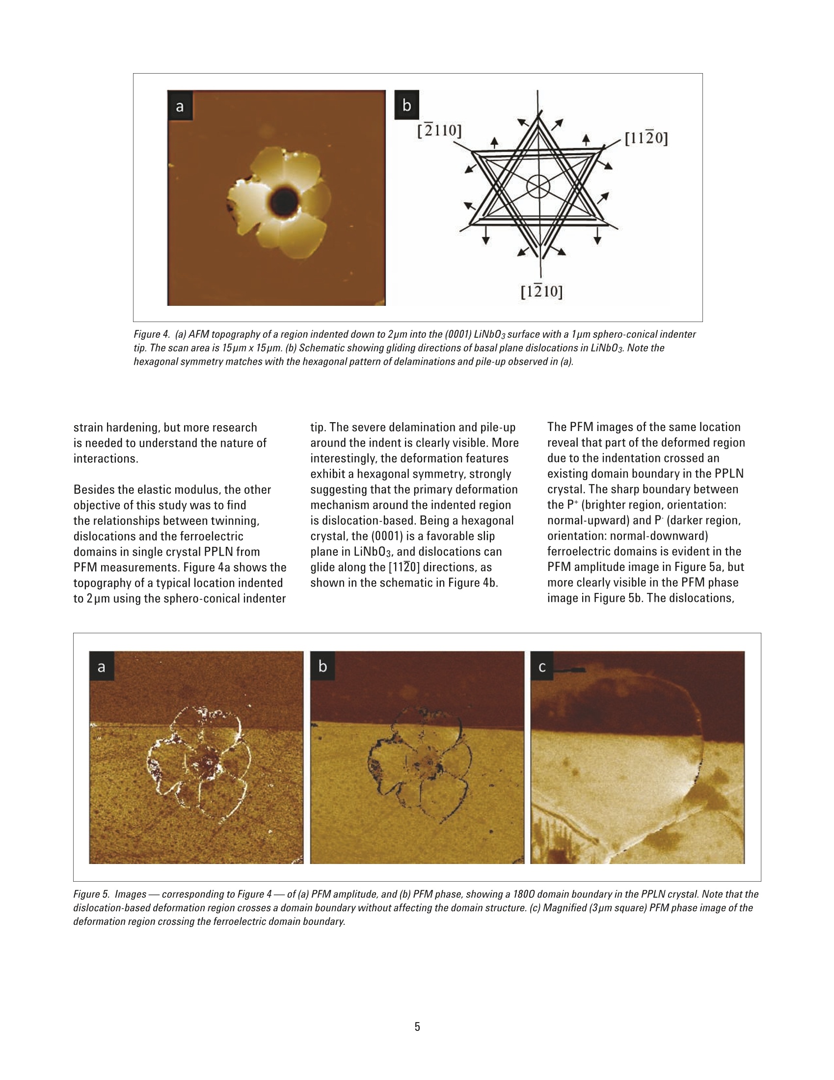
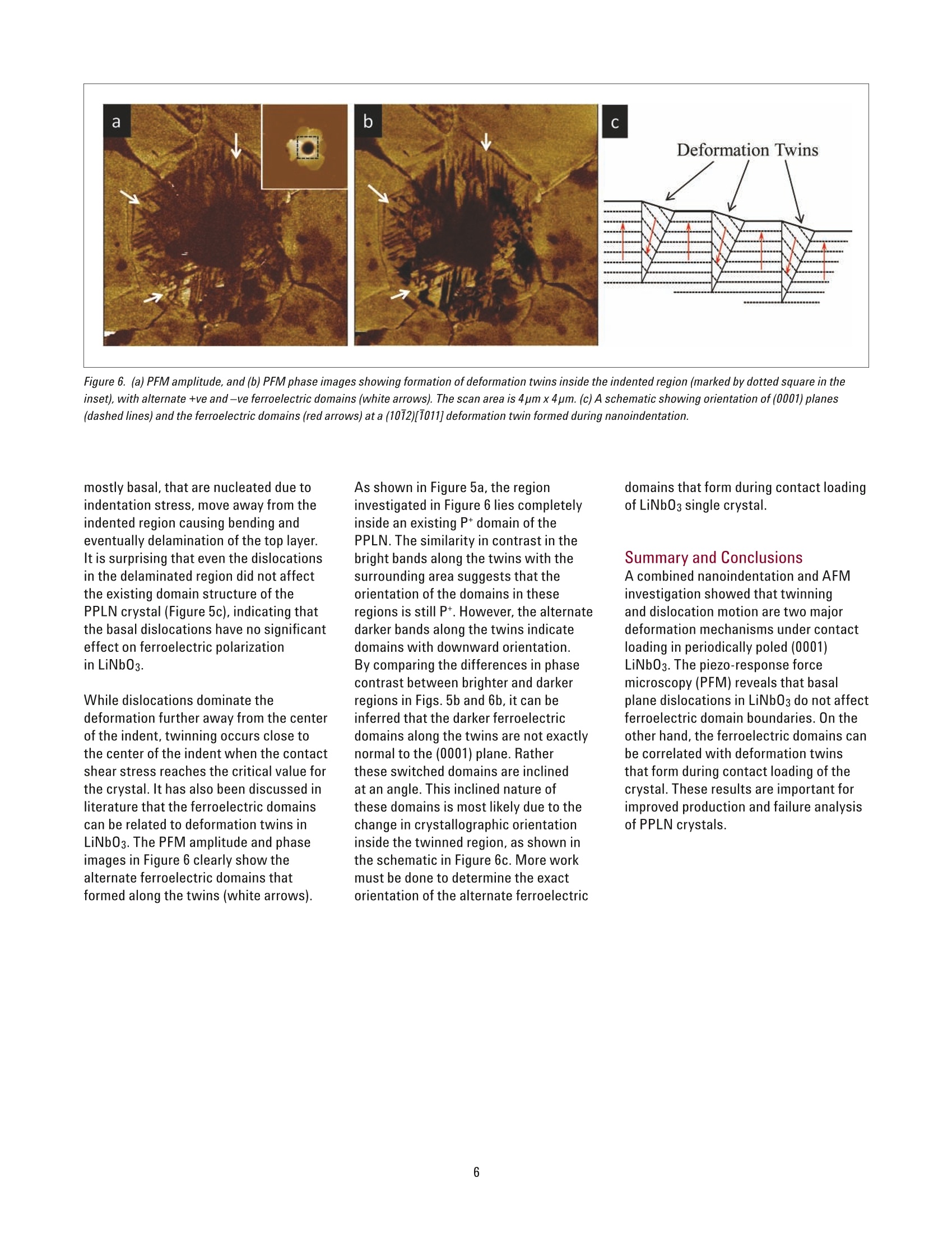
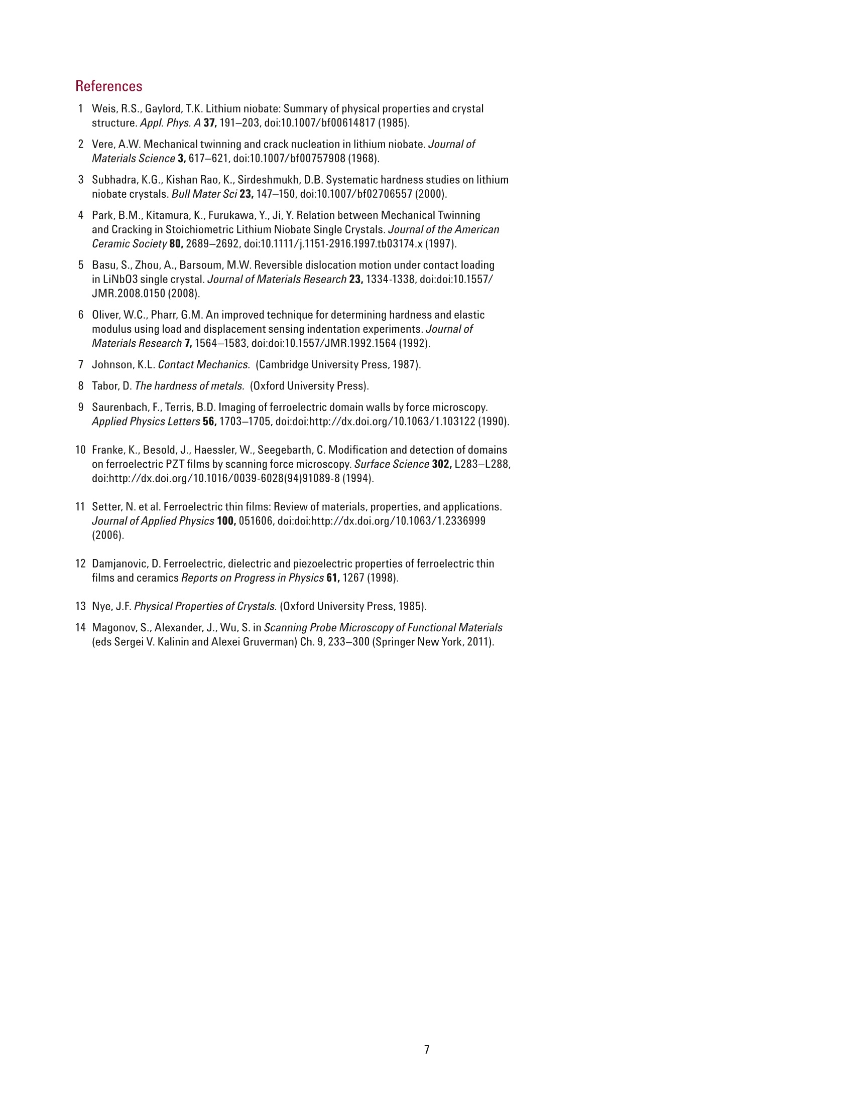
Contact Deformation of LiNb03 Single Crystal:Dislocations, Twins and Ferroelectric Domains Application Note Sandip Basu and Shijie Wu Reliability of many Lithium niobate—LiNb03-optoelectronic devicesdepends on proper understandingof their deformation behavior undercontact stresses that may occurduring various fabrication steps. Thisstudy addresses this need by using ananoindentation method to determinethe critical shear stress needed for thetransition from pure elastic to elastic-plastic deformation. The transitionstresses determined during this studyare lower than the theoretical shearstrength, indicating the presenceand distribution of defect nucleationcenters those formed during the crystalgrowth or fabrication processes. Wedemonstrate here that (1012)[1011] twinsform underneath the indented region,whereas dislocation based deformationis dominant further away from the centerof the indent. Piezo-response forcemicroscopy (PFM) revealed that whilethe dislocations nucleated during contactloading do not interact with existingferroelectric domains, the deformationtwins near the center of the indent formnew domains with inverted polarization. Introduction LiNb03 has important nonlinearoptical properties for applications inelectro-optic, acousto-optic, and opticalstorage devices. These crystals areoften periodically poled (PPLN)-withP* and P. domains with a period ofabout 5 to 35pm - for nonlinear opticsapplications. Precise knowledge of themechanical deformation of LiNb03 undercontact loading is a prerequisite forsuccessful manufacturing and operationof these single crystal devices. Despitethe importance, very little is availableon the elastic-plastic transition anddislocation movement during contactdeformation in LiNb03. Earlier studies on LiNb03 singlecrystals have been limited to mostlyuniaxial compression? and Vickersmicrohardness. When single crystalsare loaded in uniaxial compression attemperatures >1150°C, (1012)[1011]twins form. Within these twins.basal slip is observed. More recently,Park et al.4 confirmed the existence ofthis twin system. Recently,researchershave also demonstrated reversible Agilent Technologies dislocation motion in LiNb03 singlecrystal during cyclic nanoindentationexperiments.5However, little isknown about the effect of mechanicaldeformation mechanisms—especiallytwinning and dislocations - on theferroelectric domains in LiNb03. Herein,we characterize the formation of twinsand dislocation structures duringnanoindentation in a (0001) PPLNcrystal. In order to characterize themechanical behavior, we first study theelastic to elastic-plastic transition byspherical nanoindentation. Subsequentcharacterization ofthe domain structureswere carried out using piezo forcemicroscopy (PFM). Before discussingthe particular results for LiNb03, thefollowing sections briefly review thenanoindentation and atomic forcemicroscopy methods used duringthis study. Nanoindentation: Theory and Experimental DetailsThe nanoindentation experiments onthe (0001) PPLN crystal were carriedout at room temperature using a G200Nanolndenter, fitted with a diamondsphero-conical indenter with 1 pmapicalradius. The strain rate during loading waskept constant at 0.05/sec. The contactstiffness was measured by applyinga harmonic force modulation with thecontinuous stiffness measurement(CSM) attachment, during the completeloading segment. This method enablesmeasurement of the contact stiffness asa continuous function of displacementduring indenting a material. Themeasured load (P). displacement (ht)and contact harmonic stiffness (S) werethen analyzed according to Hertziancontact mechanics, as discussed below.The contact depth (hc) was calculatedaccording to the Oliver-Pharr model: where, e is a constant with a valueof 0.75 for a spherical indenter. It isimportant to note here that this equationcan be applied in both elastic andelastic-plastic regimes to calculate thecontact depth. Once the contact depthwas known, the contact radius (a) wascalculated as: where, R is the tip radius. Accordingto the theory of elastic contacts, thecontact radius is related to the harmoniccontact stiffness by: where,E* is the reduced modulus that isa function of both the sample and the tip,and can be expressed as: E and v are Young’s modulus andPoisson's ratio, respectively. Thesubscript 'i'represents the propertiesof the diamond tip, which has a Young’smodulus of 1140 GPa, and a Poisson'sratio of 0.07. Hence, for the elastic regime, themodulus of the sample can be measuredfrom the slope of an S vs. a curve, whichshould be linear based on Eqn. 3. Now,the representative indentation stress’was calculated as:8 A representative 'indentation strain’canalso be expressed by: In the elastic regime, the indentationstress is a linear function of theindentation strain. Note that a rigorous expression of strainfor elastic-plastic indentation is still verymuch a topic of ongoing discussion. Piezoresponse Force Microscopy(PFM): Theory and ExperimentalDetailsPiezoresponse Force Microscopy(PFM) has become a popular techniquefor nanoscale characterizationof ferroelectric and piezoelectricmaterials.9-11 It is based on the conversepiezoelectric effect where piezoelectricmaterials change their dimensions whensubjected to an external electric field.The strain S; developed in a piezoelectricmaterial by the applied electric fieldE; is described by the following matrixequation: S=diEi (8)where di; is the piezoelectric coefficientwith the unit of m/V. The indices i =1, 2, 3 andj=1, 2, 3...6 denotes thedirection of the electric field and thetensor component of the strain followingthe Voigt notation.13In general, indices1,2, and 3 indicate components alongthe x, y, and z axis of an orthogonalcoordinate system, and indices 4, 5,and 6 indicate shear components of thestrain tensor. The axes of the coordinatesystem are often conveniently alignedwith the crystallographic axes of acrystal. In the case of ceramics and thinfilms, the z axis is usually aligned withthe direction of the polarization, or thedirection normal to the plane of the film.The piezoelectric coefficient measuredalong the direction of the applied field isalso called the longitudinal piezoelectricconstant, and that being perpendicularto the electric field are called transversepiezoelectric constants. Therefore, thelongitudinal piezoelectric constant, d33.can be determined by measuring thedisplacement (Az) of the piezoelectricmaterial along the direction of the appliedfield (E3): Az= d33V (9) assuming S3=Az/zoand E3=V/zo, whereV is the applied voltage and zo is thethickness of the sample. The measureddisplacement will be positive, i.e. Figure 1. Nanoindentation load-displacement response from 5 different locations on (0001)LiNb03surface, indented with a sphero-conical indenter of 1pm tip radius. Note the distinct pop-in eventsmarking the transition from elastic to elastic-plastic deformation. expansion, if the polarization direction isparallel to the applied field, and it will benegative if the polarization direction isantiparallel to the applied field. With PFM, a conductive AFM cantileveris scanned across the surface of apiezoelectric sample in contact mode.The conductive cantilever also servesas the top electrode to provide thepolarization field to the sample. Thesample can be either connected to abottom electrode or floating. In the casethe sample is connected to a bottomelectrode, the electric bias can be appliedto the sample as well. In PFM experiment, an ac voltagemodulation, V=Vac cos(wt), is appliedto the conductive AFM tip, thedisplacement thus measured, accordingto equation (9), will be with d=0, for P (polarization pointing downwards)d=n, for P+ (polarization pointing upwards) Therefore, when a small ac modulationbeing added to the applied electric field,the piezoresponse will oscillate in-phasewith the ac modulation signal if thepolarization is parallel to the field, andout-phase if antiparallel. Consequentlya lock-in amplifier can be used toanalyze the piezoresponse signal andto determine both the magnitude ofthe displacement and the polarizationdirection of the sample. The detection oflongitudinal piezoresponse is also called.vertical piezoresponse force microscopy(VPFM). The presence of non-zero transversepiezoelectric constants, e.g. di5, and thepossible misalignment of polarization tothe applied field due to random crystalorientation, an electric field normal tothe surface can also cause in-planeshear deformation. This in-plane sheardeformation of the sample will giverise to a torsion-like motion to the AFMcantilever, thus results in a change inthe friction signal (or the lateral forcesignal). In a way similar to VPFM, alock-in amplifier can be used to detect the in-plane piezoresponse signal ALinduced by an ac voltage modulation: (11) where deff is the effective in-planepiezoresponse constant, and d is thephase angle related to polarizationdirection. For antiparallel domainsthe phase angle will be 180° indifference. The measurement ofin-plane piezoresponse is often calledlateral piezoresponse force microscopy(LPFM).4 In this study, post-indentationtopography was examined using a5600LS Atomic Force Microscope(AFM). The ferroelectric domains ofthe indent structure were imaged usingPFM capability implemented in the AFMThe conductive cantilever used is a Pt-coated cantilever with a force constantof 2.8N/m. An ac modulation voltageof 4volts peak-to-peak at 12kHz wasapplied to acquire the PFM signal. Results and DiscussionsThe load-displacement response forthe 1pm indentation on the (0001)PPLN clearly exhibits three distinctregimes of deformation- a fully elasticdeformation, followed by pop-ins (or,displacement bursts), and subsequentelastic-plastic deformation. The pop-insrepresents the transition from elasticto elastic-plastic deformation. So,before the pop-in the deformation iscompletely linear elastic as discussed inthe literature. The elastic modulus canthus be measured from the slope of thecontact stiffness vs. contact radius plotas shown in Figure 2a. At 207±2GPa,the elastic modulus measured fromthis spherical nanoindentationmethod is comparable with Berkovichnanoindentation measurement(200±2GPa) on the same surface. Figure 2. (a) The contact harmonic stiffness as a linear function of contact radius before the pop-in. (b) Indentationstress-strain curves corresponding to the load-displacement response shown in Figure 1. The dotted line represents the linearslope from which the elastic modulus was measured. The linear elastic behavior is also evidentfrom the indentation stress-straincurve shown in Figure 2b. The elasticmodulus measured from the linear slopeis 197±16 GPa. The agreement betweenmodulus measurements from differentdata sets is noteworthy and validatesthese calculations. Although the stress-strain calculations beyond the maximumpop-in load are debatable, these curvescan be extremely useful for comparisonbetween different length scales anddifferent defect population in singlecrystals. It is possible to calculate the maximumshear stress under the indenter from: The maximum shear stress occurs at adepth of about 0.48 times the contactradius under the contact surface.Figure 3 shows a distribution of themaximum shear stresses during pop-infrom 25 measurements. Although thepop-ins occur at a lower stress than thetheoretical shear strength of the crystal(G/2m), this information can be usedto monitor the defect population duringmanufacturing and application ofthese crystals. The pop-ins during nanoindentation canbe caused by different mechanisms,such as dislocation nucleationand propagation, twinning, phasetransformation,etc. However, theremay be some relationship between thestatistical distribution of maximumshear stresses at pop-ins to the exactdeformation mechanism. Therefore,more work is needed to establish suchcharacteristic parameters. With theinformation from the SEM observations reported in literature, it is reasonable toconclude that in case of LiNb03 twinningalong the (1012)[1011] system occurs.From crystallography, these twins formin a triangular pattern, and the numberof twin bands increases with increasingload (or, stress) underneath the indenter.Beyond the pop-in, the bending of basalplanes also causes dislocations tonucleate and glide further away from theindented region. The interaction betweenthe dislocations may cause the observed Figure 3. Distribution of maximum shear stress during the pop-in events when (0001) LiNb03 wasindented with a 1pm sphero-conical indenter. The dotted line shows the theoretical shear strength ofthe material. Figure 4. (a) AFM topography of a region indented down to 2pm into the (0001)LiNb03surface with a 1pm sphero-conical indentertip. The scan area is 15pm x 15pm. (b) Schematic showing gliding directions of basal plane dislocations in LiNb03. Note thehexagonal symmetry matches with the hexagonal pattern of delaminations and pile-up observed in (a). strain hardening, but more researchis needed to understand the nature ofinteractions. Besides the elastic modulus, the otherobjective of this study was to findthe relationships between twinning,dislocations and the ferroelectricdomains in single crystal PPLN fromPFM measurements. Figure 4a shows thetopography of a typical location indentedto 2 pm using the sphero-conical indenter tip. The severe delamination and pile-uparound the indent is clearly visible. Moreinterestingly, the deformation featuresexhibit a hexagonal symmetry, stronglysuggesting that the primary deformationmechanism around the indented regionis dislocation-based. Being a hexagonalcrystal, the (0001) is a favorable slipplane in LiNb03, and dislocations canglide along the [1120] directions, asshown in the schematic in Figure 4b. The PFM images of the same locationreveal that part of the deformed regiondue to the indentation crossed anexisting domain boundary in the PPLNcrystal. The sharp boundary betweenthe P+ (brighter region, orientation:normal-upward) and P. (darker region,orientation: normal-downward)ferroelectric domains is evident in thePFM amplitude image in Figure 5a, butmore clearly visible in the PFM phaseimage in Figure 5b. The dislocations, Figure 5. Images-corresponding to Figure 4- of (a) PFM amplitude, and (b) PFM phase, showing a 1800 domain boundary in the PPLN crystal. Note that thedislocation-based deformation region crosses a domain boundary without affecting the domain structure. (c) Magnified (3pm square) PFM phase image of thedeformation region crossing the ferroelectric domain boundary. ab C Figure 6. (a) PFM amplitude, and (b) PFM phase images showing formation of deformation twins inside the indented region (marked by dotted square in theinset), with alternate +ve and -ve ferroelectric domains (white arrows). The scan area is 4pm x4pm.(c) A schematic showing orientation of (0001) planes(dashed lines) and the ferroelectric domains (red arrows) at a (1012)[1011] deformation twin formed during nanoindentation. mostly basal, that are nucleated due toindentation stress, move away from theindented region causing bending andeventually delamination of the top layer.It is surprising that even the dislocationsin the delaminated region did not affectthe existing domain structure of thePPLN crystal (Figure 5c), indicating thatthe basal dislocations have no significanteffect on ferroelectric polarizationin LiNb03. While dislocations dominate thedeformation further away from the centerof the indent, twinning occurs close tothe center of the indent when the contactshear stress reaches the critical value forthe crystal. It has also been discussed inliterature that the ferroelectric domainscan be related to deformation twins inLiNb03. The PFM amplitude and phaseimages in Figure 6 clearly show thealternate ferroelectric domains thatformed along the twins (white arrows). As shown in Figure 5a, the regioninvestigated in Figure 6 lies completelyinside an existing P* domain of thePPLN. The similarity in contrast in thebright bands along the twins with thesurrounding area suggests that theorientation of the domains in theseregions is still P*. However, the alternatedarker bands along the twins indicatedomains with downward orientation.By comparing the differences in phasecontrast between brighter and darkerregions in Figs. 5b and 6b, it can beinferred that the darker ferroelectricdomains along the twins are not exactlynormal to the (0001) plane.Ratherthese switched domains are inclinedat an angle.This inclined nature ofthese domains is most likely due to thechange in crystallographic orientationinside the twinned region, as shown inthe schematic in Figure 6c. More workmust be done to determine the exactorientation of the alternate ferroelectric domains that form during contact loadingof LiNb03single crystal. Summary and ConclusionsA combined nanoindentation and AFMinvestigation showed that twinningand dislocation motion are two majordeformation mechanisms under contactloading in periodically poled (0001)LiNb03. The piezo-response forcemicroscopy(PFM) reveals that basalplane dislocations in LiNb03 do not affectferroelectric domain boundaries.On theother hand, the ferroelectric domains canbe correlated with deformation twinsthat form during contact loading of thecrystal. These results are important forimproved production and failure analysisof PPLN crystals. References 1 Weis, R.S., Gaylord, T.K. Lithium niobate: Summary of physical properties and crystalstructure.Appl. Phys. A 37, 191-203, doi:10.1007/bf00614817 (1985). 2Vere,A.W. Mechanical twinning and crack nucleation in lithium niobate.Journal ofMaterials Science 3, 617-621, doi:10.1007/bf00757908 (1968). 3Subhadra, K.G., Kishan Rao, K., Sirdeshmukh, D.B. Systematic hardness studies on lithiumniobate crystals. Bull Mater Sci 23, 147-150,doi:10.1007/bf02706557(2000). 4Park, B.M., Kitamura,K., Furukawa,Y.,Ji, Y. Relation between Mechanical Twinningand Cracking in Stoichiometric Lithium Niobate Single Crystals.Journal of the AmericanCeramic Society 80, 2689-2692,doi:10.1111/j.1151-2916.1997.tb03174.x(1997). 5Basu, S.,Zhou, A., Barsoum, M.W. Reversible dislocation motion under contact loadingin LiNb03 single crystal. Journal of Materials Research 23,1334-1338, doi:doi:10.1557/JMR.2008.0150 (2008). 6Oliver, W.C., Pharr, G.M. An improved technique for determining hardness and elasticmodulus using load and displacement sensing indentation experiments. Journal ofMaterials Research 7,1564-1583, doi:doi:10.1557/JMR.1992.1564 (1992). ( 7 J ohnson, K.L. Contact Mechanics. ( C ambridge University Press, 1987). ) ( 8 T abor, D. The hardness of metals. (Oxford Un i versity Pr e ss). ) 9Saurenbach, F., Terris, B.D. Imaging of ferroelectric domain walls by force microscopy.Applied Physics Letters 56, 1703-1705, doi:doi:http://dx.doi.org/10.1063/1.103122 (1990). 10 Franke, K., Besold, J., Haessler,W., Seegebarth, C. Modification and detection of domainson ferroelectric PZT films by scanning force microscopy. Surface Science 302, L283-L288,doi:http://dx.doi.org/10.1016/0039-6028(94)91089-8(1994). 11 Setter,N. et al. Ferroelectric thin films: Review of materials,properties, and applications.Journal of Applied Physics 100,051606, doi:doi:http://dx.doi.org/10.1063/1.2336999(2006). 12 Damjanovic,D. Ferroelectric, dielectric and piezoelectric properties of ferroelectric thinfilms and ceramics Reports on Progress in Physics 61, 1267(1998). 13 Nye, J.F. Physical Properties of Crystals. (Oxford University Press, 1985). 14 Magonov, S., Alexander, J.,Wu, S. in Scanning Probe Microscopy of Functional Materials(eds Sergei V. Kalinin and Alexei Gruverman) Ch. 9, 233-300 (Springer New York, 2011). Nanomeasurement Systems fromAgilent Technologies Agilent Technologies, the premiermeasurement company,offers high-precision, modular nanomeasurementsolutions for research, industry,andeducation. Exceptional worldwide supportis provided by experienced applicationscientists and technical service personnel.Agilent’s leading-edge R&D laboratoriesensure the continued, timely introductionand optimization of innovative,easy-to-usenanomeasure system technologies. www.agilent.com/find/nano Americas Canada (877)894 4414 Latin America 305 269 7500 United States (800) 829 4444 Asia Pacific Australia 1800629485 China 800 810 0189 Hong Kong 800938 693 India 1800112929 Japan 0120(421)345 Korea 0807690800 Malaysia 1800888 848 Singapore 1 800 375 8100 Taiwan 0800047866 Thailand 1800226008 Europe & Middle East Austria 43 (0)1 360 277 1571 Belgium 32(0)24049340 Denmark 45 7013 1515 Finland 358 (0)10 8552100 France 0825010700* *0.125E/minuteGermany 49(0)7031 4646333Ireland 1890924204Israel 972-3-9288-504/544ltaly 390292608484Netherlands 31 (0)20547 2111 Spain 34 (91)631 3300 Sweden 0200-882255 Switzerland 0800805353 United Kingdom 44(0)1189276201 Other European Countries: www.agilent.com/find/contactus Product specifications and descriptions in this documentsubject to change without notice. CAgilent Technologies, Inc. 2013 Published in USA. November 1,2013 5991-3520EN
确定

还剩6页未读,是否继续阅读?

广州贝拓科学技术有限公司为您提供《Contact Deformation of LiNbO3 Single Crystal:Dislocations, Twins and Ferroelectric Domains》,该方案主要用于其他中--检测,参考标准--,《Contact Deformation of LiNbO3 Single Crystal:Dislocations, Twins and Ferroelectric Domains》用到的仪器有
相关方案
更多