


方案详情
文
In summary, we have performed a complete Raman polarized study of a single GaN nanowire using a confocal microscope together with a high resolution stage. The high spatial resolution of our Raman confocal instrument together with a piezoelectric stage demonstrates unambiguously the possibility to image the optical properties of nanoobjects with a resolution better than 200 nm keeping the full advantages of the polarization control under a confocal microscope.
方案详情

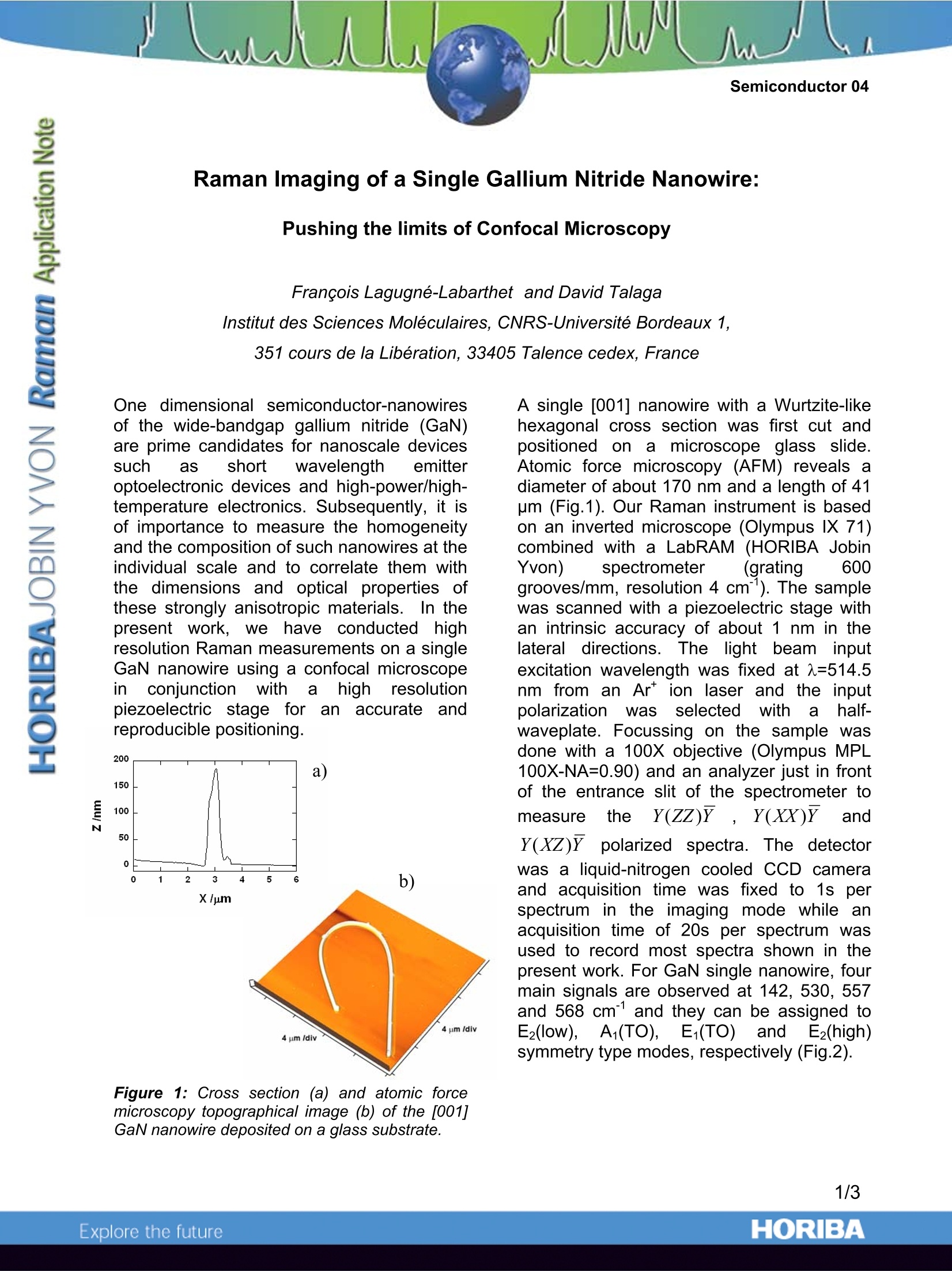
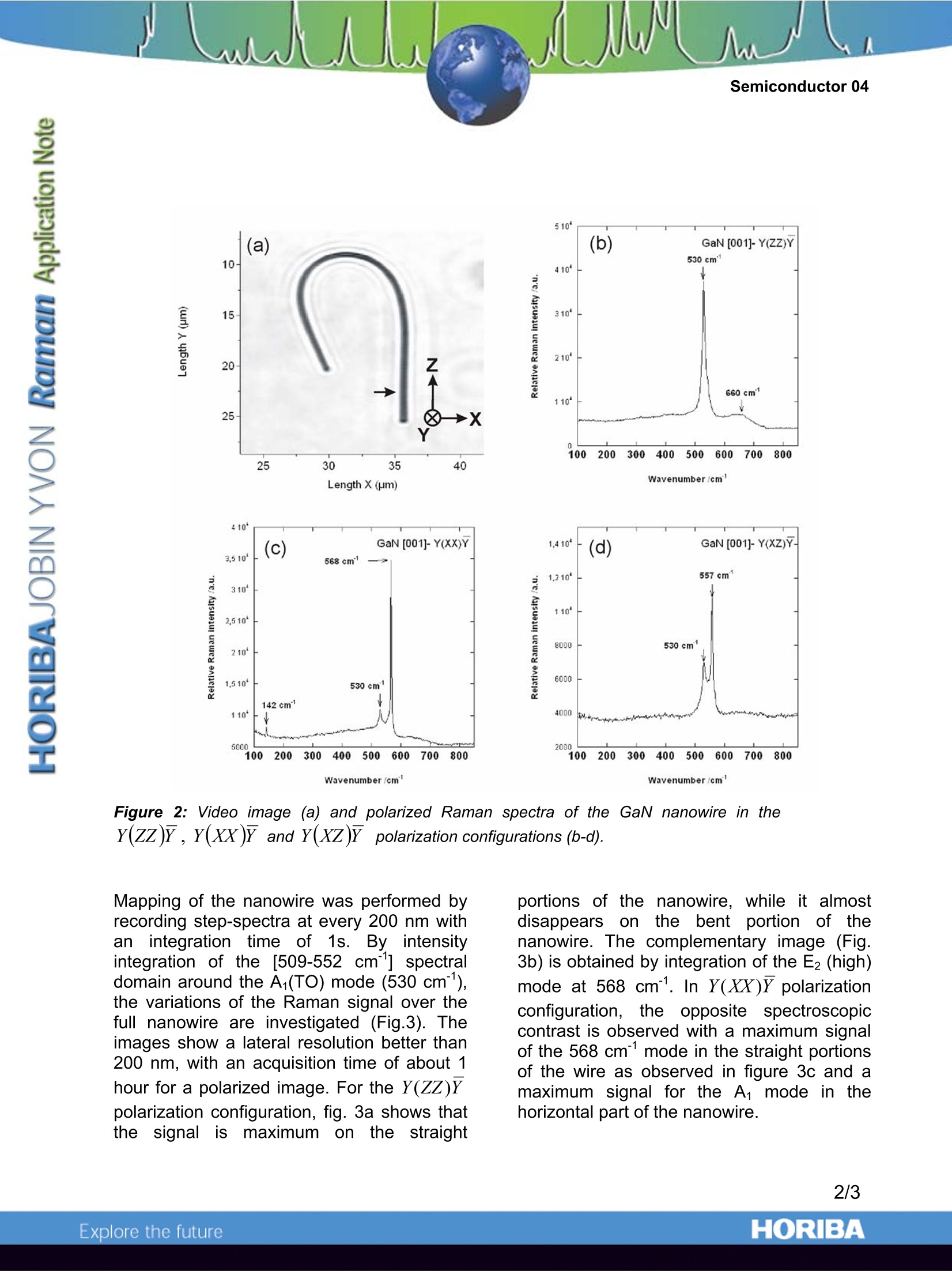
Raman Imaging of a Single Gallium Nitride Nanowire:Pushing the limits of Confocal Microscopy Francois Lagugne-Labarthet and David TalagaInstitut des Sciences Moleculaires,CNRS-Universite Bordeaux 1, 351 cours de la Liberation, 33405 Talence cedex, France One dimensional semiconductor-nanowiresof the wide-bandgap gallium nitride (GaN)are prime candidates for nanoscale devicessuch as short wavelength emitteroptoelectronic devices and high-power/high-temperature electronics. Subsequently, it isof importance to measure the homogeneityand the composition of such nanowires at theindividual scale and to correlate them withthe dimensions and optical properties ofthese strongly anisotropic materials. In thepresent work,.wehave conducted highresolution Raman measurements on a singleGaN nanowire using a confocal microscopeinconjunction with highresolutionpiezoelectric stage foranaccurate andreproducible positioning. Figure 1: Cross section (a) and atomic forcemicroscopy topographical image (b) of the [001]GaN nanowire deposited on a glass substrate. A single [001] nanowire with a Wurtzite-likehexagonal cross section was first cut andpositioned on a microscope glass slide.Atomic force microscopy (AFM) reveals adiameter of about 170 nm and a length of 41um (Fig.1). Our Raman instrument is basedon an inverted microscope (Olympus IX 71)combined with a LabRAM1 (HORIBA JobinYvon) spectrometer (grating 600grooves/mm, resolution 4 cm). The samplewas scanned with a piezoelectric stage withan intrinsic accuracy of about 1 nm in thelateral directions.The light beamiinputexcitation wavelength was fixed at A=514.5nm from an Ar ion laser and the inputpolarization wassgselectedwith a half-waveplate. Focussing on the sample wasdone with a 100X objective (Olympus MPL100X-NA=0.90) and an analyzer just in frontof the entrance slit of the spectrometer tomeasure the Y(ZZ)Y, Y(XX)Y andY(XZ)Y polarized spectraa.. TTheh edetectorwas a liquid-nitrogen cooled CCD cameraand acquisition time was fixed to 1s; perspectrum in the imaging mode while anacquisition time of 20s per spectrum wasused to record most spectra shown in thepresent work. For GaN single nanowire, fourmain signals are observed at 142, 530, 557and 568 cm and they can be assigned toE2(low),,A(TO), E(TO) and E2(high)symmetry type modes, respectively (Fig.2). Figure 2: Video image (a) and polarized Raman spectra of the GaN nanowire in theY(ZZ)Y,Y(XX)Y and Y(XZ)Y polarization configurations (b-d). Mapping of the nanowire was performed byrecording step-spectra at every 200 nm withan integration time of 1s. By intensityintegration of the [509-552 cm"'] spectraldomain around the A(TO) mode (530 cm"'),the variations of the Raman signal over thefull nanowire are investigated (Fig.3). Theimages show a lateral resolution better than200 nm, with an acquisition time of about 1hour for a polarized image. For the Y(ZZ)Ypolarization configuration, fig. 3a shows thatthe signalismaximum on|1the straight portions of the nanowire, while it almostdisappears ontthe bentportion of thenanowire. The complementary image (Fig.3b) is obtained by integration of the E2 (high)mode at 568 cm". In Y(XX)Y polarizationconfiguration, the opposite spectroscopiccontrast is observed with a maximum signalof the 568 cm’mode in the straight portionsof the wire as observed in figure 3c and amaximum signal for the A mode in thehorizontal part of the nanowire. Lengthx(pm Figure 3: Polarized Raman images generated by integration of the [509-552 cm'] (a) and [558-575cm'](b) spectral ranges for Y(ZZ)Y polarization configuration. Polarized Raman images generated byintegration [509-552 cm'] (c) and [558-575cm] (d)spectral ranges for Y(XX)Y polarizationconfiguration. In summary, we have performed a completeRaman polarized study of a single GaNusinnanowire usingana confocalmicroscopetogether with a high resolution stage. Thehigh spatial resolution of our Raman confocalinstrument together with a piezoelectric stagedemonstrates unambiguously the possibilityto image the optical properprcties of nano-objects with a resolution better than 200 nm keepinggthe full advantages of thepolarization control under a iconfocalmicroscope. Reference: "Polarized) Ramani ConfocalMicroscopy ofSingle Gallium NitrideNanowires", P.J. Pauzauskie, D.Talaga, K.Seo, P.Yang, F.Lagugne-Labarthet, J. Am.Chem. Soc., 2005,127(49), 17146. ORIBAExplore the future ORIBAExplore the future In summary, we have performed a complete Raman polarized study of a single GaN nanowire using a confocal microscope together with a high resolution stage. The high spatial resolution of our Raman confocal instrument together with a piezoelectric stage demonstrates unambiguously the possibility to image the optical properties of nanoobjects with a resolution better than 200 nm keeping the full advantages of the polarization control under a confocal microscope.
确定

还剩1页未读,是否继续阅读?

HORIBA(中国)为您提供《GaN纳米线中拉曼成像检测方案(激光拉曼光谱)》,该方案主要用于其他中拉曼成像检测,参考标准--,《GaN纳米线中拉曼成像检测方案(激光拉曼光谱)》用到的仪器有
相关方案
更多
该厂商其他方案
更多