


方案详情
文
Graphene is a new nanomaterial which may partially replace silicon in microcircuits and computer chips in the future. In order to better understand its quality characteristics, fast reliable techniques that deliver the right property measures are needed. Raman spectroscopy has emerged as a key technique for studying this exceptional material.
方案详情

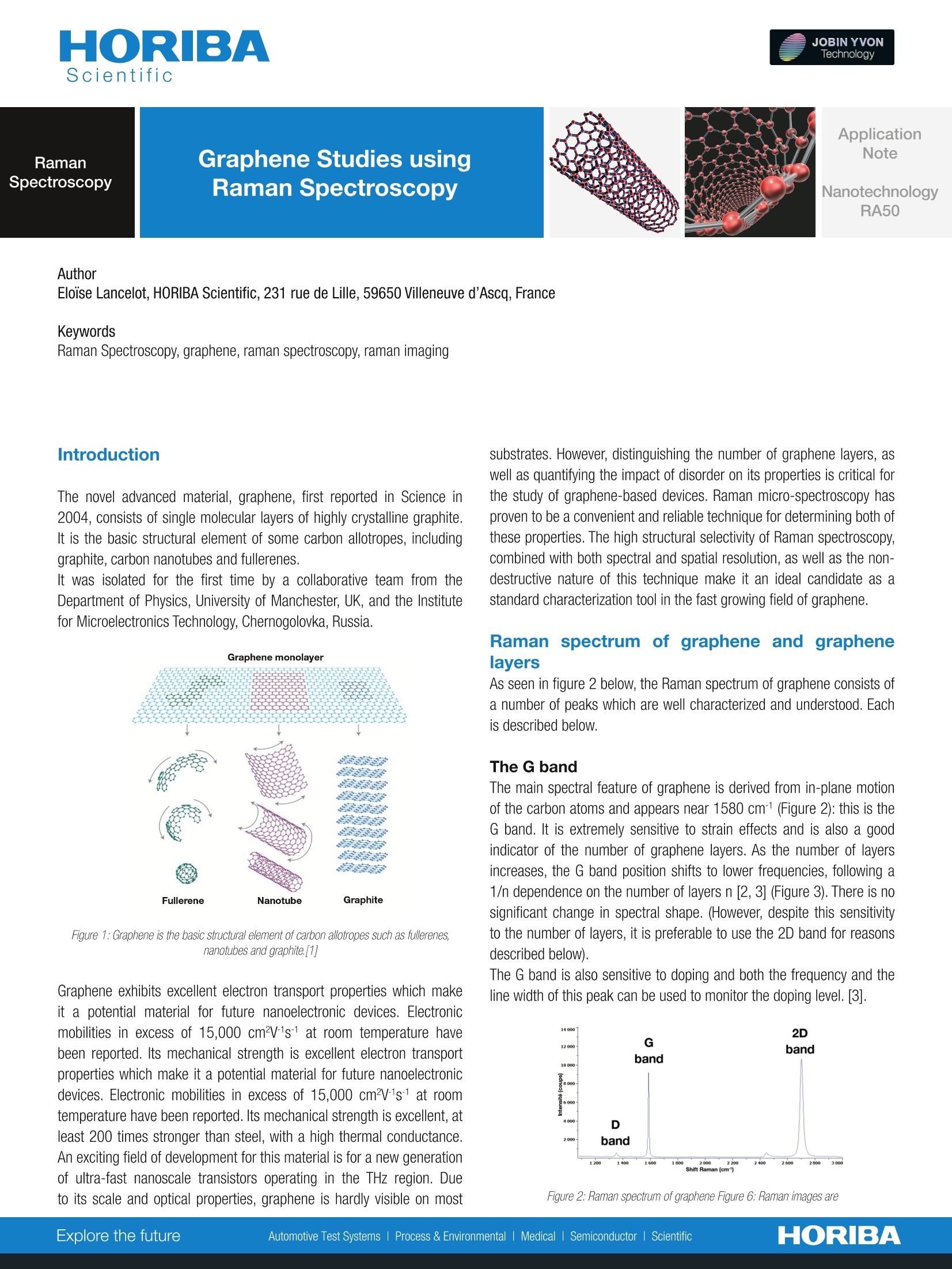
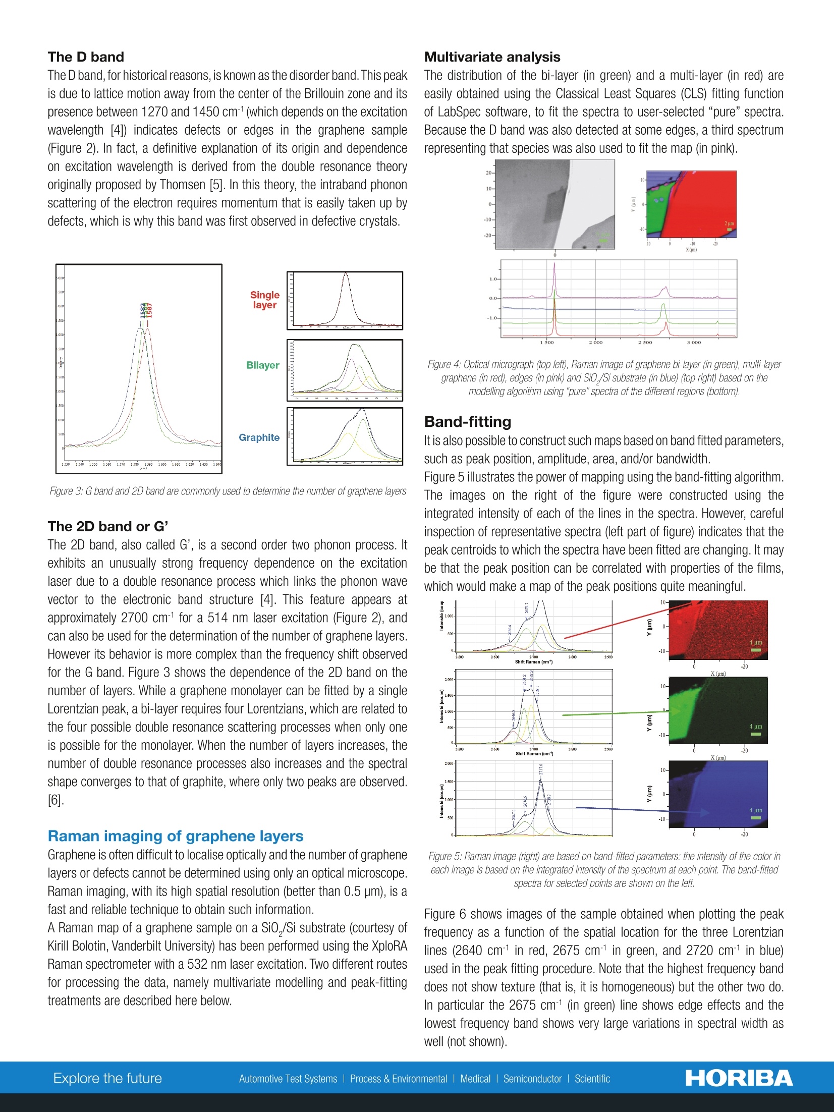
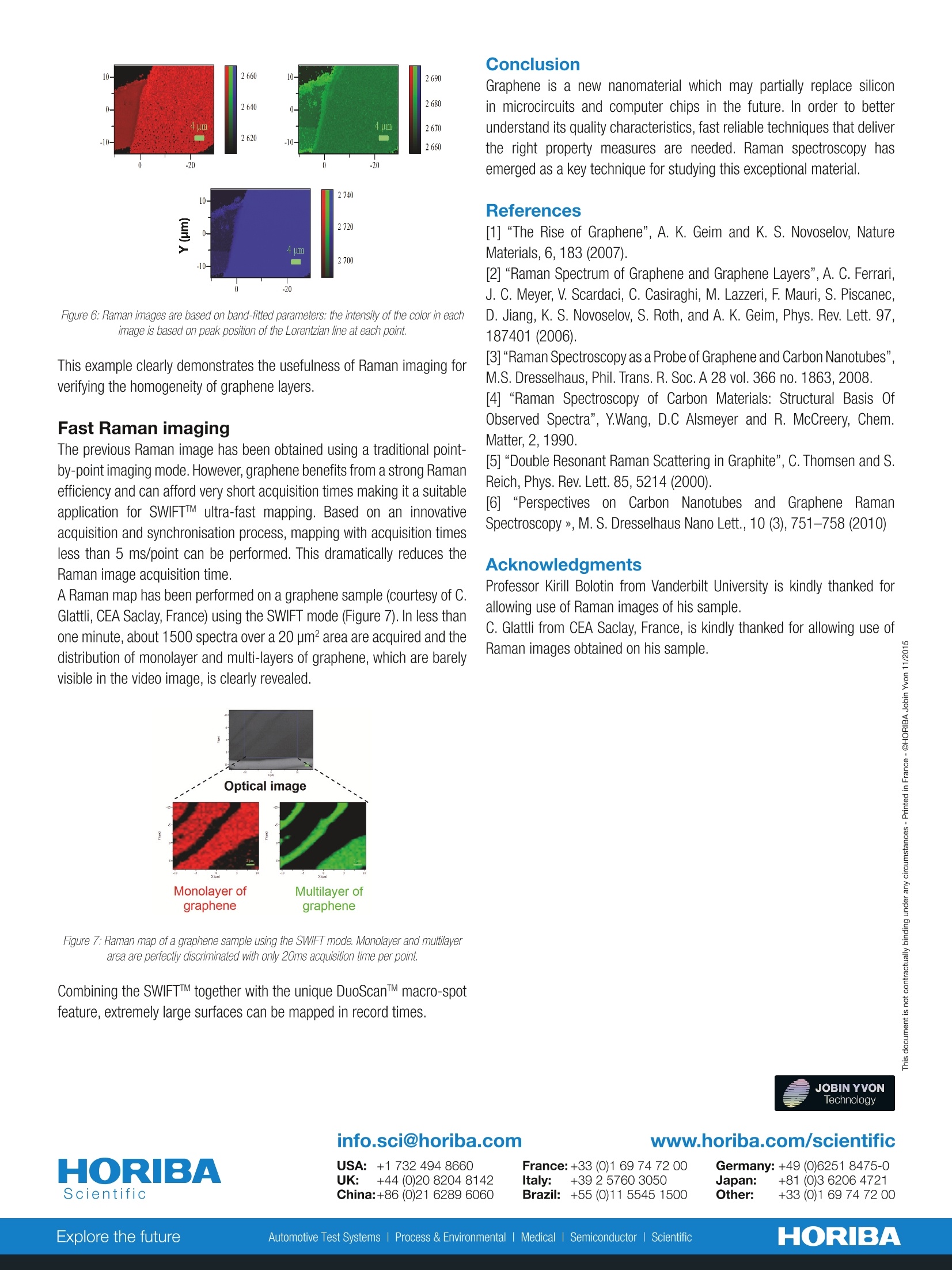
HORIBAScientific :UK: +44 (0)208204 8142 ApplicationNoteNanotechnologyRA50 Author Eloise Lancelot, HORIBA Scientific, 231 rue de Lille, 59650 Villeneuve d'Ascq, France Keywords Introduction The novel advanced material, graphene, first reported in Science in2004, consists of single molecular layers of highly crystalline graphite.It is the basic structural element of some carbon allotropes, includinggraphite, carbon nanotubes and fullerenes. lt was isolated for the first time by a collaborative team from theDepartment of Physics, University of Manchester, UK, and the Institutefor Microelectronics Technology, Chernogolovka, Russia Figure 1: Graphene is the basic structural element of carbon allotropes such as fullerenes,nanotubes and graphite.[1] Graphene exhibits excellent electron transport properties which makeit a potential material for future nanoelectronic devices. Electronicmobilities in excess of 15,000 cm2V1s at room temperature havebeen reported. Its mechanical strength is excellent electron transportproperties which make it a potential material for future nanoelectronicdevices. Electronic mobilities in excess of 15,000 cm2V1s1 at roomtemperature have been reported. Its mechanical strength is excellent, atleast 200 times stronger than steel, with a high thermal conductance.An exciting field of development for this material is for a new generationof ultra-fast nanoscale transistors operating in the THz region. Dueto its scale and optical properties, graphene is hardly visible on most substrates. However, distinguishing the number of graphene layers, aswell as quantifying the impact of disorder on its properties is critical forthe study of graphene-based devices. Raman micro-spectroscopy hasproven to be a convenient and reliable technique for determining both ofthese properties. The high structural selectivity of Raman spectroscopy,combined with both spectral and spatial resolution, as well as the non-destructive nature of this technique make it an ideal candidate as astandard characterization tool in the fast growing field of graphene. 1anspectrum of graphene and graphenelayers As seen in figure 2 below, the Raman spectrum of graphene consists ofa number of peaks which are well characterized and understood. Eachis described below. The G band The main spectral feature of graphene is derived from in-plane motionof the carbon atoms and appears near 1580 cm(Figure 2): this is theG band. It is extremely sensitive to strain effects and is also a goodindicator of the number of graphene layers. As the number of layersincreases, the G band position shifts to lower frequencies, following a1/n dependence on the number of layers n [2, 3] (Figure3). There is nosignificant change in spectral shape. (However, despite this sensitivityto the number of layers, it is preferable to use the 2D band for reasonsdescribed below). The G band is also sensitive to doping and both the frequency and theline width of this peak can be used to monitor the doping level. [3]. . Figure 2: Raman spectrum of graphene Figure 6: Raman images are The D band The D band, for historical reasons, is known as the disorder band.This peakis due to lattice motion away from the center of the Brillouin zone and itspresence between 1270 and 1450 cm-1(which depends on the excitationwavelength [4]) indicates defects or edges in the graphene sample(Figure 2). In fact, a definitive explanation of its origin and dependenceon excitation wavelength is derived from the double resonance theoryoriginally proposed by Thomsen [5]. In this theory, the intraband phononscattering of the electron requires momentum that is easily taken up bydefects, which is why this band was first observed in defective crystals. Figure 3: G band and 2D band are commonly used to determine the number of graphene layers The 2D band or G’ The 2D band, also called G', is a second order two phonon process. ltexhibits an unusually strong frequency dependence on the excitationlaser due to a double resonance process which links the phonon wavevector to the electronic band structure [4]. This feature appears atapproximately 2700 cm for a 514 nm laser excitation (Figure 2), andcan also be used for the determination of the number of graphene layers.However its behavior is more complex than the frequency shift observedfor the G band. Figure 3 shows the dependence of the 2D band on thenumber of layers. While a graphene monolayer can be fitted by a singleLorentzian peak, a bi-layer requires four Lorentzians, which are related tothe four possible double resonance scattering processes when only oneis possible for the monolayer. When the number of layers increases, thenumber of double resonance processes also increases and the spectralshape converges to that of graphite, where only two peaks are observed.6]. Raman imaging of graphene layers Graphene is often difficult to localise optically and the number of graphenelayers or defects cannot be determined using only an optical microscope.Raman imaging, with its high spatial resolution (better than 0.5 pm), is afast and reliable technique to obtain such information. A Raman map of a graphene sample on a SiO,/Si substrate (courtesy ofKirill Bolotin, Vanderbilt University) has been performed using the XploRARaman spectrometer with a 532 nm laser excitation. Two different routesfor processing the data, namely multivariate modelling and peak-fittingtreatments are described here below. Multivariate analysis The distribution of the bi-layer (in green) and a multi-layer (in red) areeasily obtained using the Classical Least Squares (CLS) fitting functionof LabSpec software, to fit the spectra to user-selected “pure"spectra.Because the D band was also detected at some edges, a third spectrumrepresenting that species was also used to fit the map (in pink). Figure4: Optical micrograph (top left), Raman image of graphene bi-layer (in green), multi-/ayergraphene (in red), edges (in pink) and SiO,/Si substrate (in blue) (top right) based on themodelling algorithm using "pure" spectra of the different regions (bottom). Band-fitting It is also possible to construct such maps based on band fitted parameters,such as peak position, amplitude, area,and/or bandwidth. Figure 5 illustrates the power of mapping using the band-fitting algorithm.The images on the right of the figure were constructed using theintegrated intensity of each of the lines in the spectra. However, carefulinspection of representative spectra (left part of figure) indicates that thepeak centroids to which the spectra have been fitted are changing. It maybe that the peak position can be correlated with properties of the films,which would make a map of the peak positions quite meaningful. Figure 5: Raman image (right) are based on band-fitted parameters: the intensity of the color ineach image is based on the integrated intensity of the spectrum at each point. The band-fittedspectra for selected points are shown on the left. Figure 6 shows images of the sample obtained when plotting the peakfrequency as a function of the spatial location for the three Lorentzianlines (2640 cm1 in red, 2675 cm in green, and 2720 cm in blue)used in the peak fitting procedure. Note that the highest frequency banddoes not show texture (that is, it is homogeneous) but the other two do.In particular the 2675 cm1(in green) line shows edge effects and thelowest frequency band shows very large variations in spectral width aswell (not shown). Figure 6: Raman images are based on band-fitted parameters: the intensity of the color in eachimage is based on peak position of the Lorentzian line at each point. This example clearly demonstrates the usefulness of Raman imaging forverifying the homogeneity of graphene layers. Fast Raman imaging The previous Raman image has been obtained using a traditional point-by-point imaging mode. However, graphene benefits from a strong Ramanefficiency and can afford very short acquisition times making it a suitableapplication for SWIFTIM ultra-fast mapping. Based on an innovativeacquisition and synchronisation process, mapping with acquisition timesless than 5 ms/point can be performed. This dramatically reduces theRaman image acquisition time. A Raman map has been performed on a graphene sample (courtesy of C.Glattli, CEA Saclay, France) using the SWIFT mode (Figure 7). In less thanone minute, about 1500 spectra over a 20 pm? area are acquired and thedistribution of monolayer and multi-layers of graphene, which arebarelyvisible in the video image, is clearly revealed. Conclusion Graphene is a new nanomaterial which may partially replace siliconin microcircuits and computer chips in the future. In order to betterunderstand its quality characteristics, fast reliable techniques that deliverthe right property measures are needed. Raman spectroscopy hasemerged as a key technique for studying this exceptional material. References [1] “The Rise of Graphene”, A. K. Geim and K. S. Novoselov, NatureMaterials, 6, 183 (2007). [2]“Raman Spectrum of Graphene and Graphene Layers", A. C. Ferrari, J.C. Meyer, V. Scardaci, C. Casiraghi, M. Lazzeri, F. Mauri, S. Piscanec, D. Jiang, K. S. Novoselov, S. Roth, and A. K. Geim, Phys. Rev. Lett. 97,187401 (2006). [3]“Raman Spectroscopy as a Probe of Graphene and Carbon Nanotubes",M.S. Dresselhaus, Phil. Trans. R. Soc. A 28 vol. 366 no. 1863,2008. [4]"Raman Spectroscopy of Carbon Materials: Structural Basis OfObserved Spectra”, Y.Wang, D.C Alsmeyer and R. McCreery, Chem.Matter, 2,1990. [5] “Double Resonant Raman Scattering in Graphite", C. Thomsen and S.Reich,Phys. Rev. Lett. 85,5214 (2000). [6] “Perspectives onCarbon Nanotubes ind Graphene RamanSpectroscopy》, M. S. Dresselhaus Nano Lett., 10 (3),751-758(2010) Acknowledgments Professor Kirill Bolotin from Vanderbilt University is kindly thanked forallowing use of Raman images of his sample. C. Glattli from CEA Saclay, France, is kindly thanked for allowing use ofRaman images obtained on his sample. Figure 7: Raman map of a graphene sample using the SWIFT mode. Monolayer and multilayerarea are perfectly discriminated with only 20ms acquisition time per point. Combining the SWIFTM together with the unique DuoScanTM macro-spotfeature, extremely large surfaces can be mapped in record times. info.sci@horiba.com www.horiba.com/scientific USA: +1732494 8660 France:+33 (0)1 69 74 72 00 Germany: +49 (0)6251 8475-0 China:+86 (0)21 6289 6060 Italy: +39257603050Japan:+81 (0)3 6206 4721Brazil: +55 (0)11 5545 1500Other:+33 (0)1 69 7472 00 HORIBAExplore the futureAutomotive Test Systems IProcess & EnvironmentalMedicalI Semiconductor l Scientific Graphene is a new nanomaterial which may partially replace silicon in microcircuits and computer chips in the future. In order to better understand its quality characteristics, fast reliable techniques that deliver the right property measures are needed. Raman spectroscopy has emerged as a key technique for studying this exceptional material.
确定
还剩1页未读,是否继续阅读?

HORIBA(中国)为您提供《石墨烯中单层分析,多层分析检测方案(激光拉曼光谱)》,该方案主要用于石墨烯中单层分析,多层分析检测,参考标准--,《石墨烯中单层分析,多层分析检测方案(激光拉曼光谱)》用到的仪器有
相关方案
更多
该厂商其他方案
更多