


方案详情
文
拉曼光谱已经成为石墨烯的表征和改性研究中必不可少的工具,在石墨烯的层数、缺陷表征,以及掺杂、堆叠、层间嵌入、环境影响等方面的研究起着非常重要的作用。拉曼成像不仅可直观的表征不同层石墨烯层数的空间分布,还可以表征石墨烯掺杂、形变引起的拉曼峰位、峰形变化的分布。
方案详情

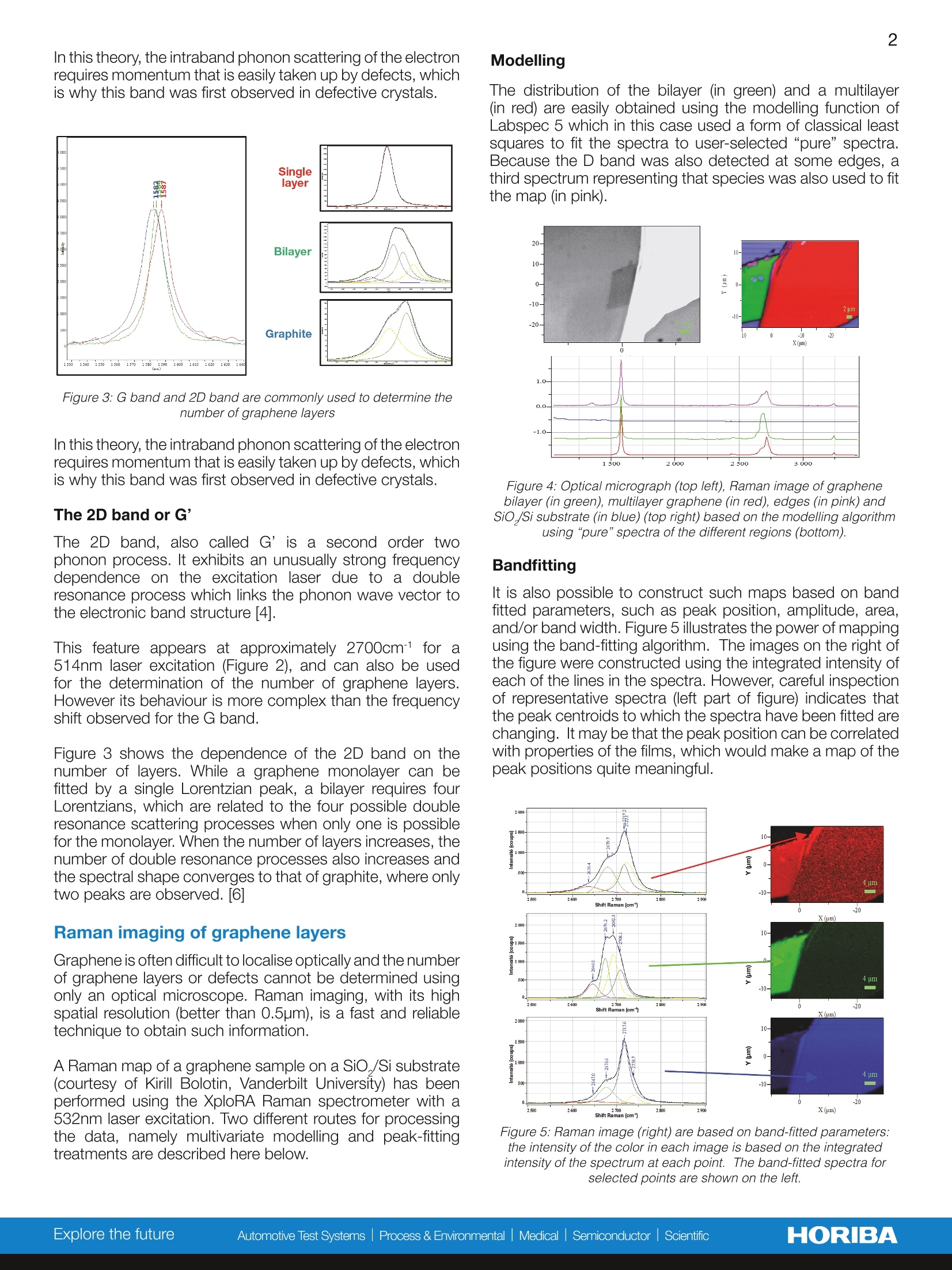
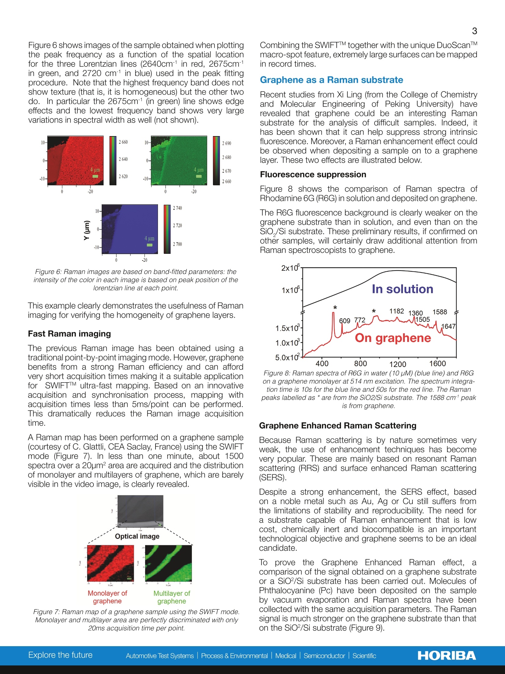
HORIBAScientific 2 Nanotechnology Raman Spectroscopy RA50 Perspectives on Raman spectroscopy of Graphene The novel advanced material, Graphene,first report in Science in 2004, consists of single molecular layersof highly crystalline graphite. It is the basic structural element of some carbon allotropes including graphite,carbon nanotubes and fullerenes. It was isolated for the first time by a collaborative team at the Department ofPhysics, University of Manchester, UK and the Institute for Microelectronics Technology Chernogolovka, Russia. Graphene exhibits excellent electrontransport properties which make it a potentiel material for future nanoelectronicdevices.Electronic mobilities in excess of 15 000 cm2V1sat room temperaturehave been reported. lts mechanical strength is excellent, at least 200 times better than steel andit has a high thermal conductance. An exciting field of development for thismaterial is for a new generation of ultra-fast nanoscale transistors operatingin the THz region. Due to its scale and optical properties,graphene is hardlyvisible on most substrates. However, distinguishing the number of graphene layers as well as quantifyingthe impact of disorder on its properties is critical for the study of graphene-based devices.Raman micro spectroscopy has proven to be a convenient andreliable technique for determining both of these properties.The high structural selectivity of Raman spectroscopy, combined with both spectral and spatial Figure 1: Graphene is the basic structuralresolution as well as the non-destructive nature of this technique make it anelement of carbon allotropes such as fulle-ideal candidate as a standard characterisation tool in the fast growing field of renes, nanotubes or graphite.[1] graphene. Raman spectrum of graphene and graphenelayers As seen in figure 2 below, the Raman spectrum of grapheneconsists of a number of peaks which are well characterisedand understood. Each is described below. The G band The main spectral feature of graphene is derived fromin-plane motion of the carbon atoms and appears near1580cm1(Figure 2): this is the G band. It is extremelysensitive to strain effects and is also a good indicator of thenumber of graphene layers. As the number of layers increases, the G band positionshifts to lower frequencies, following a 1/n dependence onthe number of layers n [2] (Figure 3). There is no significant change in spectral shape. (However,despite this sensitivity to the number of layers, it is preferableto use the 2D band for reasons described below). The G band is also sensitive to doping and both thefrequency and the line width of this peak can be used tomonitor the doping level. [3] Figure 2: Raman spectrum of graphene The D band The D band, for historical reasons is known as the disorderband. This peak is due to lattice motion away from thecenter of the Brillouin zone and its presence between1270 and 1450 cm(which depends on the excitationwavelength [4]) indicates defects or edges in the graphenesample (Figure 2). In fact, a definitive explanation of its origin and dependenceon excitation wavelength is derived from the doubleresonance theory originally proposed by Thomsen [5]. In this theory, the intraband phonon scattering of the electronrequires momentum that is easily taken up by defects, whichis why this band was first observed in defective crystals. Figure 3: G band and 2D band are commonly used to determine thenumber of graphene layers In this theory, the intraband phonon scattering of the electronrequires momentum that is easily taken up by defects, whichis why this band was first observed in defective crystals. The 2D band or G’ The 2D band, also called G’ is aa sseeccoonndd order twophonon process. It exhibits an unusually strong frequencydependence on the excitation laser due to a doubleresonance process which links the phonon wave vector tothe electronic band structure [4]. This feature appears at approximately 2700cm1 for a514nm laser excitation (Figure 2), and can also be usedfor the determination of the number of graphene layers.However its behaviour is more complex than the frequencyshift observed for the G band. Figure 3 shows the dependence of the 2D band on thenumber of layers. While a graphene monolayer can befitted by a single Lorentzian peak, a bilayer requires fourLorentzians, which are related to the four possible doubleresonance scattering processes when only one is possiblefor the monolayer. When the number of layers increases, thenumber of double resonance processes also increases andthe spectral shape converges to that of graphite, where onlytwo peaks are observed. [6] Raman imaging of graphene layers Graphene is often difficult to localise optically and the numberof graphene layers or defects cannot be determined usingonly an optical microscope. Raman imaging, with its highspatial resolution (better than 0.5um), is a fast and reliabletechnique to obtain such information. A Raman map of a graphene sample on a Sio,/Si substrate(courtesy of Kirill Bolotin, Vanderbilt University) has beenperformed using the XploRA Raman spectrometer with a532nm laser excitation. Two different routes for processingthe data, namely multivariate modelling and peak-fittingtreatments are described here below. The distribution of the bilayer (in green) and a multilayer(in red) are easily obtained using the modelling function ofLabspec 5 which in this case used a form of classical leastsquares to fit the spectra to user-selected“pure” spectra.Because the D band was also detected at some edges, athird spectrum representing that species was also used to fitthe map (in pink). Figure 4: Optical micrograph (top left), Raman image of graphenebilayer (in green), multilayer graphene (in red), edges (in pink) andSiO,/Si substrate (in blue) (top right) based on the modelling algorithmusing “pure"spectra of the different regions (bottom). Bandfitting It is also possible to construct such maps based on bandfitted parameters, such as peak position, amplitude, area,and/or band width. Figure 5 illustrates the power of mappingusing the band-fitting algorithm. The images on the right ofthe figure were constructed using the integrated intensity ofeach of the lines in the spectra. However, careful inspectionof representative spectra (left part of figure) indicates thatthe peak centroids to which the spectra have been fitted arechanging. It may be that the peak position can be correlatedwith properties of the films, which would make a map of thepeak positions quite meaningful. Figure 5: Raman image (right) are based on band-fitted parameters:the intensity of the color in each image is based on the integratedintensity of the spectrum at each point. The band-fitted spectra forselected points are shown on the left. Figure 6 shows images of the sample obtained when plottingthe peak frequency as a function of the spatial locationfor the three Lorentzian lines (2640cm1 in red, 2675cm1in green, and 2720 cm-1 in blue) used in the peak fittingprocedure. Note that the highest frequency band does notshow texture (that is, it is homogeneous) but the other twodo. In particular the 2675cm(in green) line shows edgeeffects and the lowest frequency band shows very largevariations in spectral width as well (not shown). Figure 6: Raman images are based on band-fitted parameters: theintensity of the color in each image is based on peak position of thelorentzian line at each point. This example clearly demonstrates the usefulness of Ramanimaging for verifying the homogeneity of graphene layers. Fast Raman imaging The previous Raman image has been obtained using atraditional point-by-point imaging mode. However, graphenebenefits from a strong Raman efficiency and can affordvery short acquisition times making it a suitable applicationfor SWIFTIM ultra-fast mapping. Based on an innovativeacquisition and synchronisation process, mapping withacquisition times less than 5ms/point can be performed.This dramatically reduces the Raman image acquisitiontime. A Raman map has been performed on a graphene sample(courtesy of C. Glattli, CEA Saclay,France) using the SWIFTmode (Figure 7). In less than one minute, about 1500spectra over a 20pm² area are acquired and the distributionof monolayer and multilayers of graphene, which are barelyvisible in the video image, is clearly revealed. Figure 7: Raman map of a graphene sample using the SWIFT mode.Monolayer and multilayer area are perfectly discriminated with only20ms acquisition time per point. Combining the SWIFTIM together with the unique DuoScanTMmacro-spot feature,extremely large surfaces can be mappedin recordtimes. Graphene as a Raman substrate Recent studies from Xi Ling (from the College of Chemistryand Molecular Engineering of Peking University) haverevealed that graphene could be an interesting Ramansubstrate for the analysis of difficult samples. Indeed, ithas been shown that it can help suppress strong intrinsicfluorescence.Moreover, a Raman enhancement effect couldbe observed when depositing a sample on to a graphenelayer. These two effects are illustrated below. Fluorescence suppression Figure 8 shows the comparison of Raman spectra ofRhodamine 6G (R6G) in solution and deposited on graphene. The R6G fluorescence background is clearly weaker on thegraphene substrate than in solution, and even than on theSiO,/Si substrate. These preliminary results, if confirmed onother samples, will certainly draw additional attention fromRaman spectroscopists to graphene. Figure 8: Raman spectra of R6G in water (10uM) (blue line) and R6Gon a graphene monolayer at 514 nm excitation. The spectrum integra-tion time is 10s for the blue line and 50s for the red line. The Ramanpeaks labelled as *are from the SiO2/Si substrate. The 1588 cm1 peak. is from graphene. Graphene Enhanced Raman Scattering Because Raman scattering is by nature sometimes veryweak, the use of enhancement techniques has becomevery popular. These are mainly based on resonant Ramanscattering (RRS) and surface enhanced Raman scattering(SERS). Despite a strong enhancement, the SERS effect, basedon a noble metal such as Au, Ag or Cu still suffers fromthe limitations of stability and reproducibility. The need fora substrate capable of Raman enhancement that is lowcost, chemically inert and biocompatible is an importanttechnological objective and graphene seems to be an idealcandidate. To prove the Graphene Enhanced Raman effect, acomparison of the signal obtained on a graphene substrateor a SiO/Si substrate has been carried out. Molecules ofPhthalocyanine (Pc) have been deposited on the sampleby vacuum evaporation and Raman spectra have beencollected with the same acquisition parameters. The Ramansignal is much stronger on the graphene substrate than thaton the SiO/Si substrate (Figure 9). This result seems to indicate a Raman enhancement effecton graphene. Figure 9: Comparison of the Raman spectra of Pc collected ongraphene (red line) and on the SiO/Si substrate (blue line) at632.8nm. In order to investigate the dependence of the Ramanenhancement efficiency on the number of graphene layers,Raman spectra on graphene consisting of a variablenumber of layers have been collected. The comparison in Figure 10 shows the enhancementefficiency is quite different depending on the number ofgraphene layers. It actually decreases with the increase ofthe number of graphene layers. Figure 10: The Raman spectra of Pc (a) and R6G (b) on differentnumbers of graphene layers. The blue trace is for spectra obtained ona graphene monolayer, the green one for graphene multilayers (up toabout 5), and red trace for graphite. In summary, these results show that the use of a graphenemonolayer as a Raman substrate can help to reduce thefluorescence background as well as enhance the samplespectrum by a factor ranging between 2 and 15 (spectralfeaturedependant). Instrumental specifications As seen for the different examples given in this applicationnote, an efficient characterisation of graphene samples byRaman spectroscopy calls for some specific instrumentalfeatures. A high spectral resolution is recommended todetect small frequency shifts or to effectively decomposethe 2D band in order to determine the number of layers.A reliable wavelength calibration is thus neededtocompensate for any potential variations and to ensurecorrect frequency labeling. As mentioned, there is a strongfrequency dependence on the excitation wavelength andthe use of many lasers is required in order to collect themaximum information. In addition, the power density has to be carefully selectedto avoid any photo-damage of the sample. A Ramanimaging capability is very useful to localise the differentgraphene layers and detect edge defects. The fast imagingoptions recently developed (SWIFTIM, DuoScanTM) allowsefficient mapping of very large surfaces efficiently and withconsiderable saving in acquisition times. It is worth notingthat AFM and Raman systems can be combined to accessstructural, mechanical and electrical properties of graphenesimultaneously.Tip EnhancedRaman Spectroscopy(TERS) on graphene can also be considered for revealingthe nano-scale properties of this material as well as forcharacterising the existence of localised defects. Conclusion Graphene is a new nanomaterial which may partially replacesilicon in microcircuits and computer chips in the future. Inorder to better understand its quality characteristics, fastreliable techniques that deliver the right property measuresare needed. Raman spectroscopy has emerged as a keytechnique for studying this exceptional material. It hasalso enabled the discovery of some unexpected and veryattractive properties of graphene as a Raman substrate forthe suppression of fluorescence and its enhancement ofweak Raman signals. References [1]“The rise of graphene”, A. K. Geim and K. S. Novoselov,Nature Materials, 6,183(2007). [2]“Raman spectroscopy as a probe of graphene andcarbon nanotubes", M.S. Dresselhaus, Phil. Trans. R. Soc.A 28 vol. 366 no. 1863,2008 ( [3]“Probing the Intrinsic P roperties SC of E Exfoliated Graphene:Raman Spectroscopy of Free-Standing Monolayers”, S tephane B e rciaud, Nano Lett, 9 (1), 2009 ) [4]“Raman Spectroscopy of Carbon Materials: StructuralBasis Of Observed Spectra”, Y.Wang, D.C Alsmeyer andR. McCreery, Chem.Matter, 2, 1990 [4] “Double Resonant Raman Scattering in Graphite”, C.Thomsen and S. Reich, Phys. Rev. Lett.85,5214 (2000) [6]“Perspectives on Carbon Nanotubes and GrapheneRaman Spectroscopy》, M. S. Dresselhaus Nano Lett., 10(3), 751-758 (2010) Acknowledgment C. Glattli from CEA Saclay, France, is kindly thanked forallowing use of Raman images obtained on his sample. Xi Ling, from the College of Chemistry and MolecularEngineering of Peking University is kindly thanked forallowing use of her recent results on Graphene EnhancedRaman Scattering. info-sci.fr@horiba.com www.horiba.com/scientific USA: +1 732 549 8660 France: +33 (0)16454 1300 Germany: +49 (0)89 4623 17-0UK: +44 (0)20 82048142 Italy: +39025760 3050 Japan: +81 (0)3 38618231Spain: +34 91 490 2334 China:+86(0)10 8567 9966 Brazil: +55115545 1540Other Countries:+33 (0)1 64 54 13 00 JOBIN YVONTechnologyHORIBAExplore the futureAutomotive Test SystemsProcess & EnvironmentalMedicalSemiconductorScientific
确定
还剩2页未读,是否继续阅读?

产品配置单
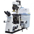
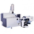
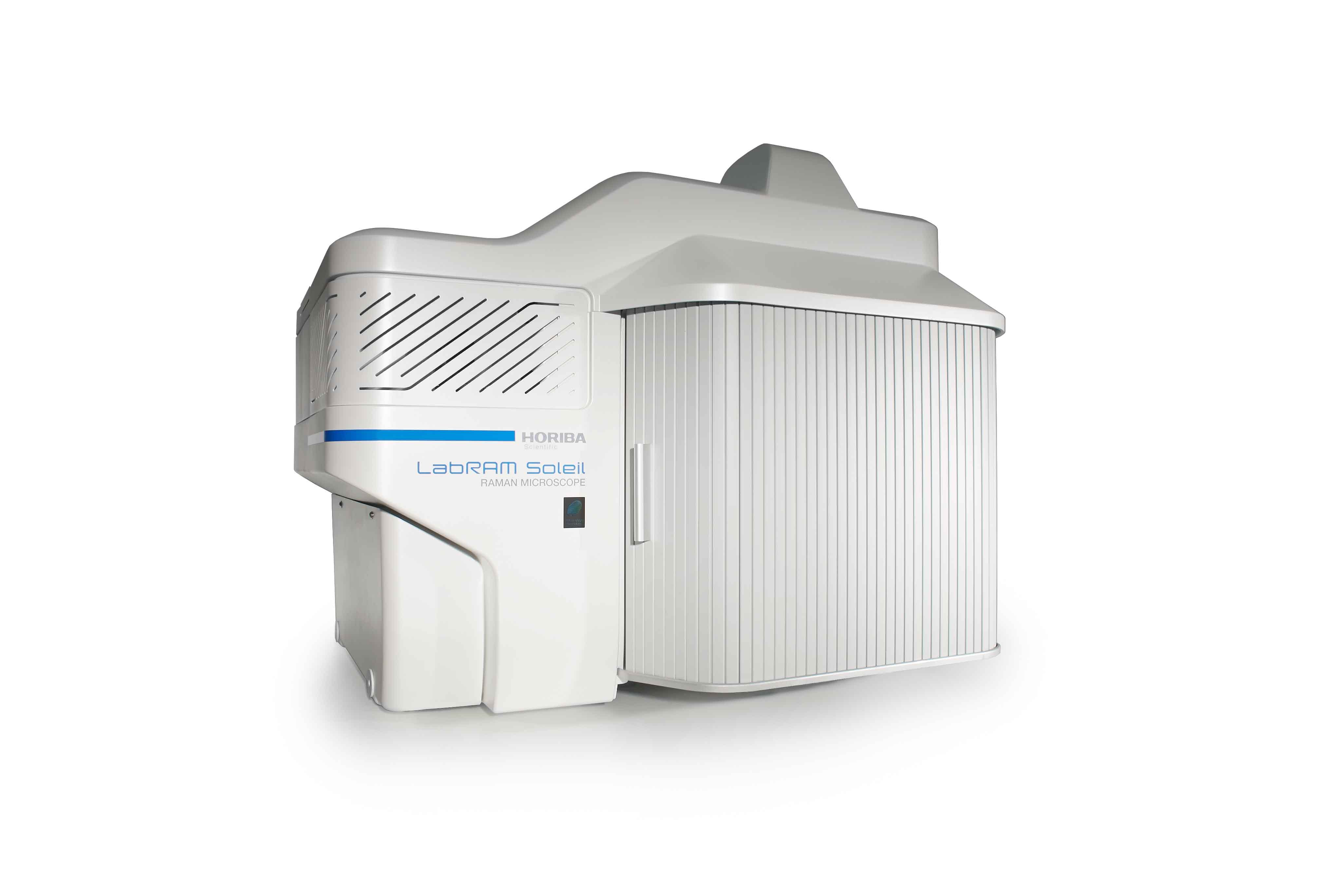
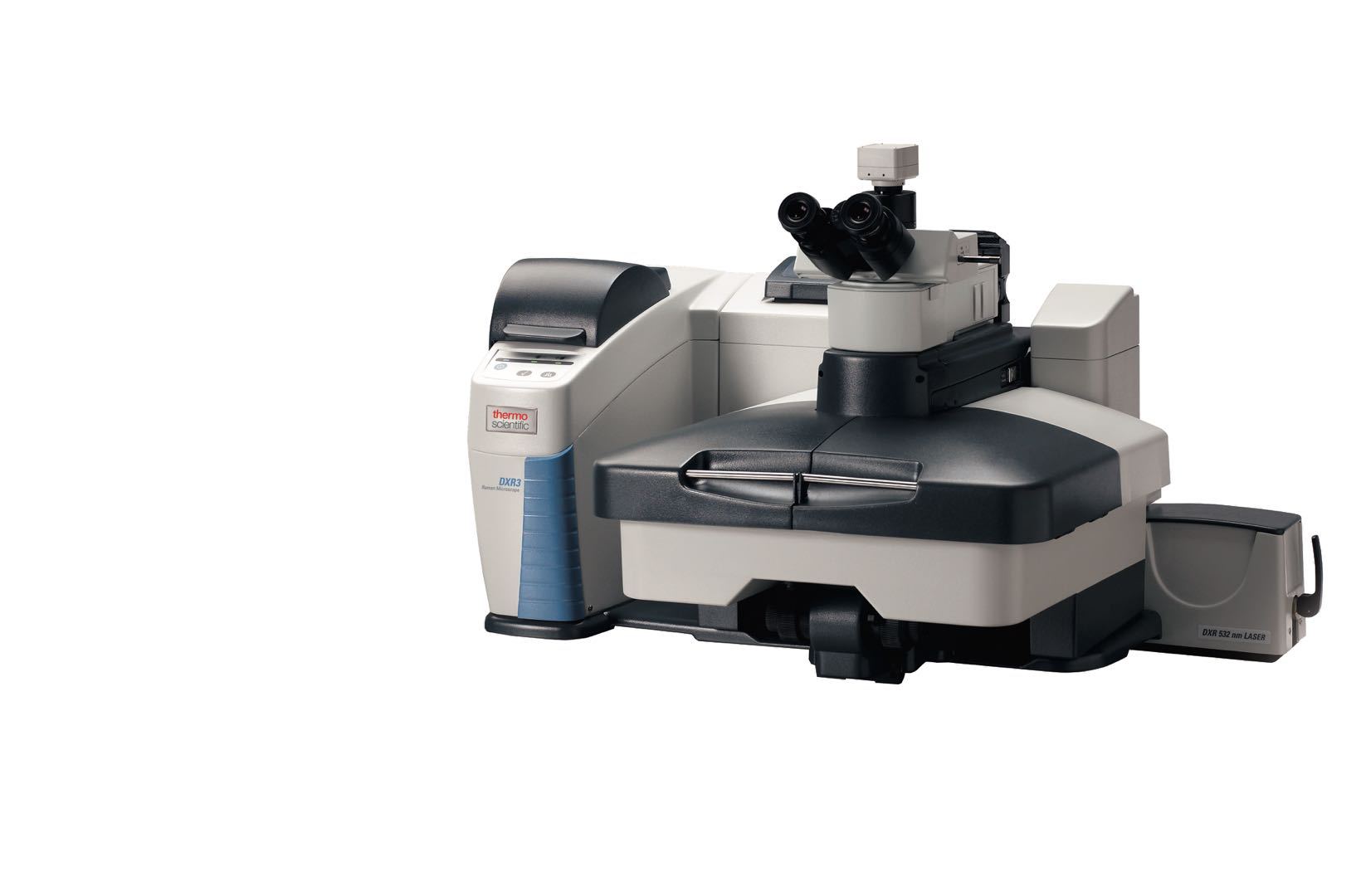
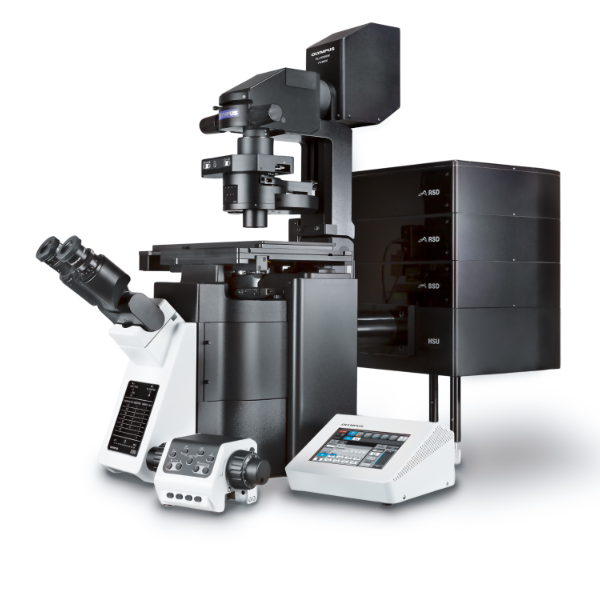
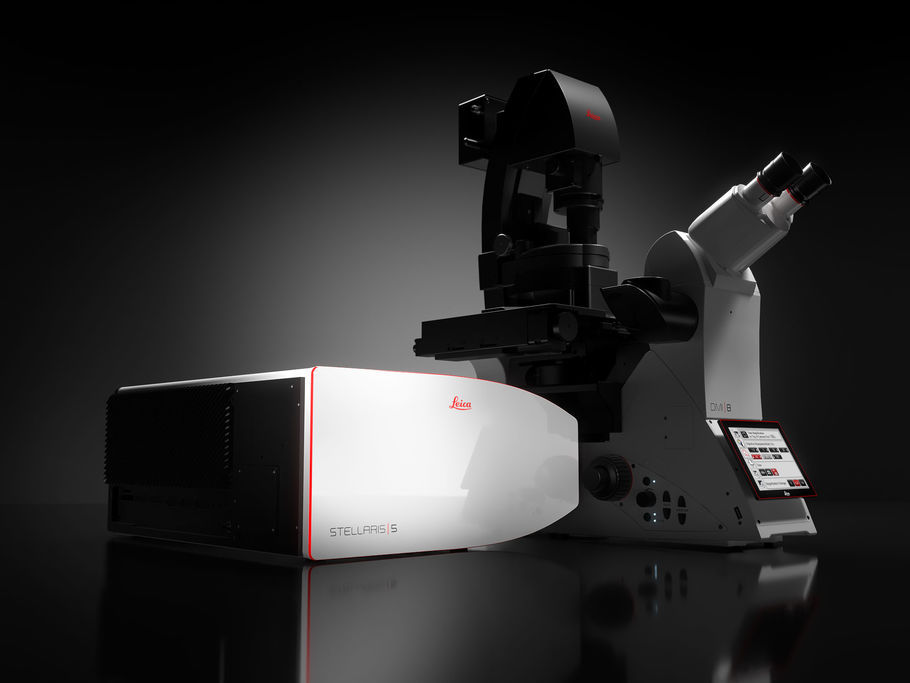
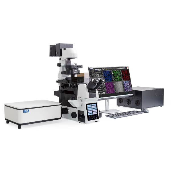
上海巨纳科技有限公司为您提供《石墨烯中层数,缺陷表征,掺杂检测方案(激光拉曼光谱)》,该方案主要用于石墨烯中层数,缺陷表征,掺杂检测,参考标准--,《石墨烯中层数,缺陷表征,掺杂检测方案(激光拉曼光谱)》用到的仪器有HORIBAXploRA INV智能型全自动拉曼光谱仪、HORIBA HR Evolution高分辨拉曼光谱仪、HORIBACombiscopeXploRA原子力拉曼联用系统、Horiba XploRA INV 多功能拉曼及成像光谱仪、HORIBA T64000三级拉曼光谱仪
推荐专场

相关方案
更多