


方案详情
文
Silmeco表面增强拉曼芯片能快速而准确的检测出爆炸品,检测方法简单,直接将被检测物放在芯片上通过拉曼光谱仪就能检测,能提前预防爆炸的发生。
方案详情

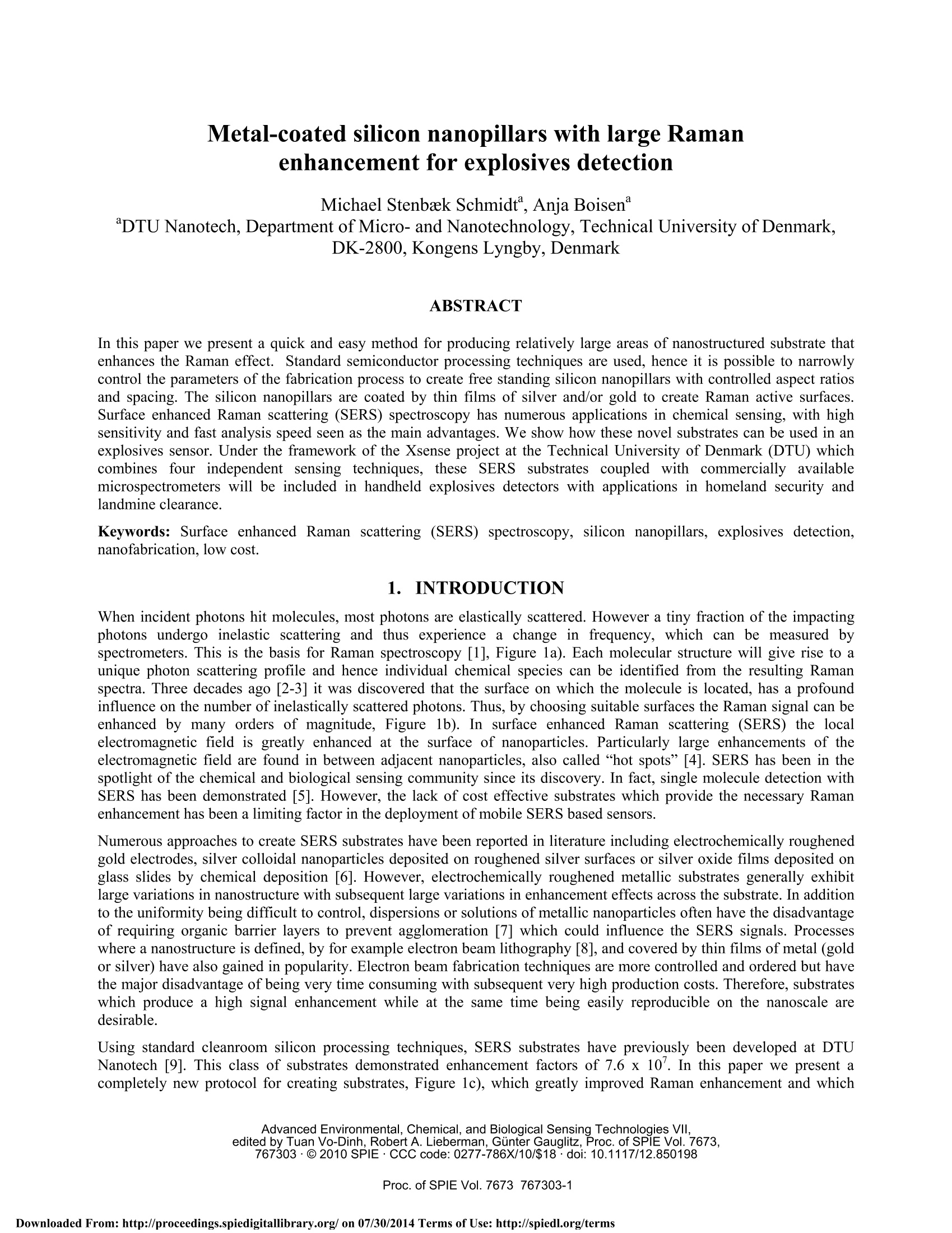
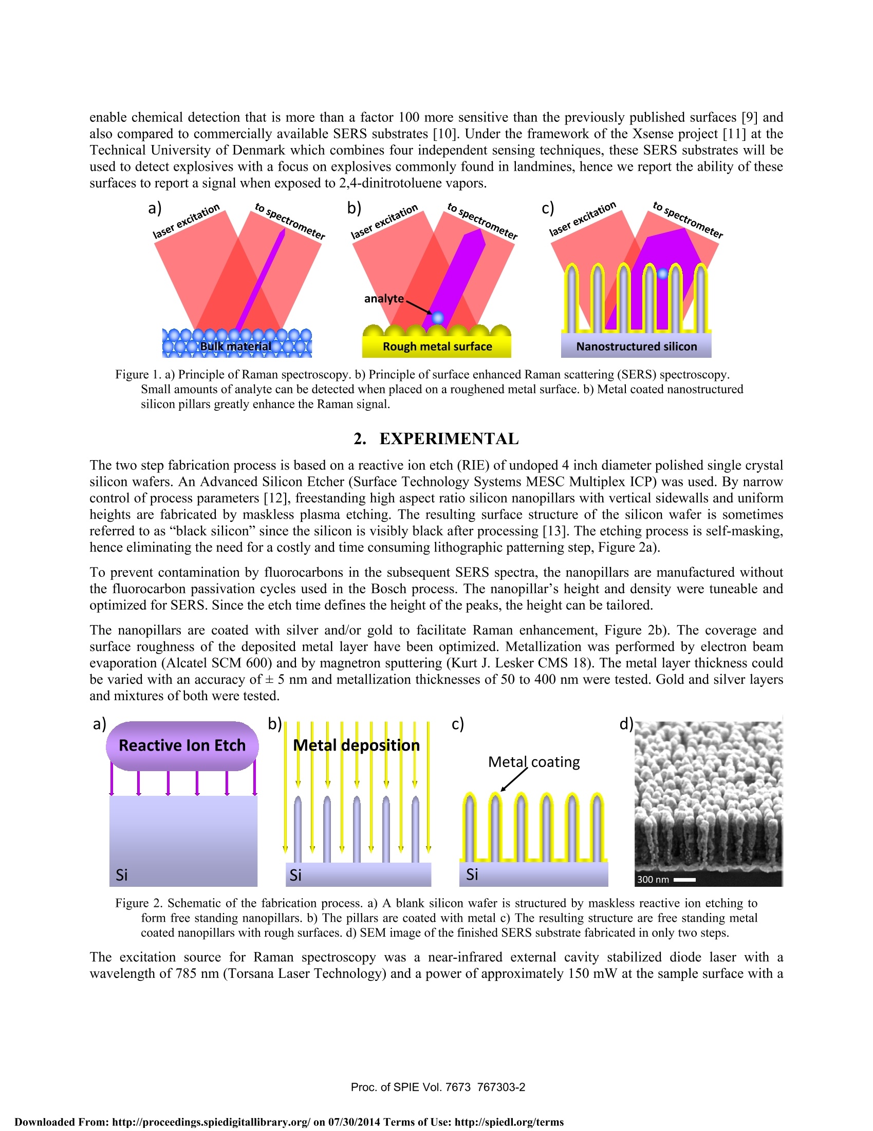
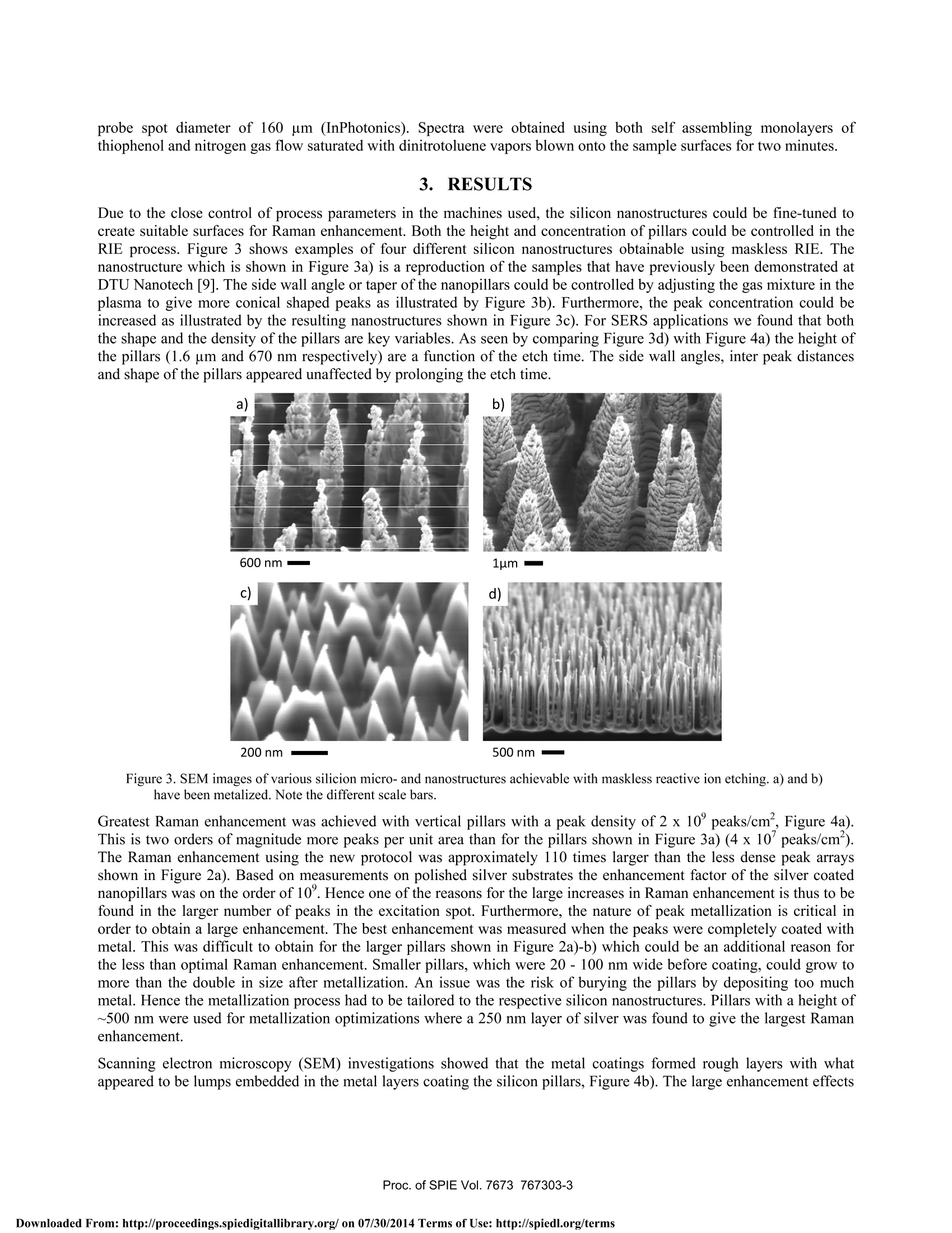
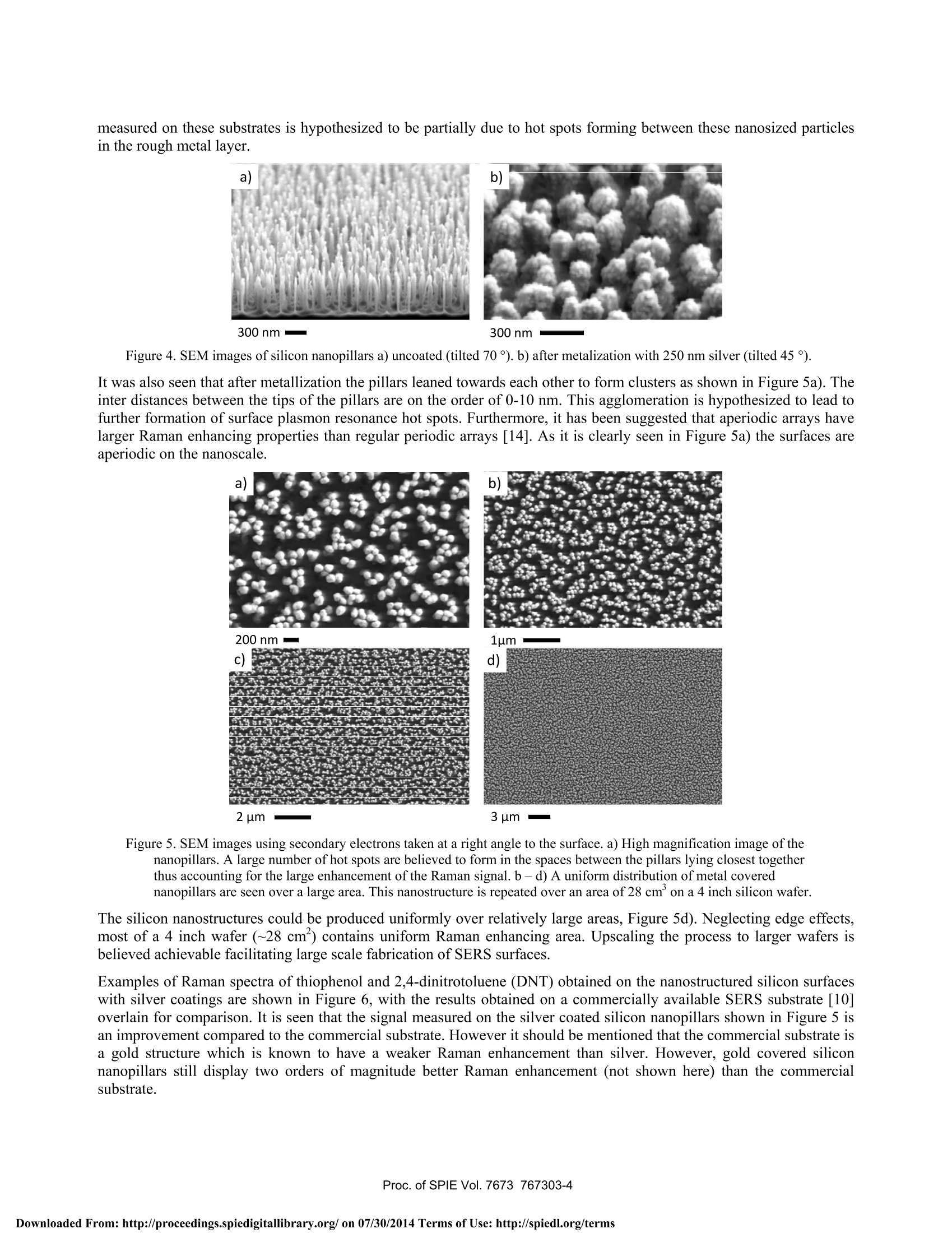
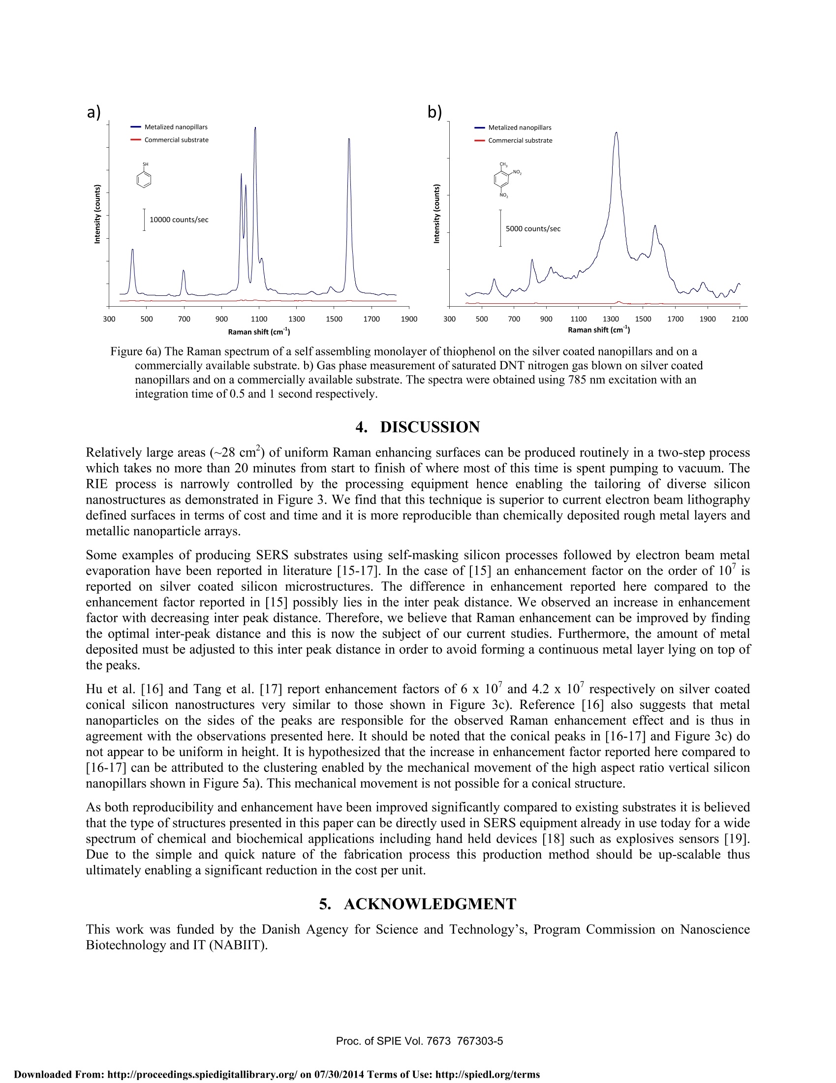
Metal-coated silicon nanopillars with large Ramanenhancement for explosives detection Michael Stenbaek Schmidt, Anja Boisen DTU Nanotech, Department of Micro- and Nanotechnology, Technical University of Denmark,DK-2800,Kongens Lyngby, Denmark ABSTRACT In this paper we present a quick and easy method for producing relatively large areas of nanostructured substrate thatenhances the Raman effect. Standard semiconductor processing techniques are used, hence it is possible to narrowlycontrol the parameters of the fabrication process to create free standing silicon nanopillars with controlled aspect ratiosand spacing. The silicon nanopillars are coated by thin films of silver and/or gold to create Raman active surfaces.Surface enhanced Raman scattering (SERS) spectroscopy has numerous applications in chemical sensing, with highsensitivity and fast analysis speed seen as the main advantages. We show how these novel substrates can be used in anexplosives sensor. Under the framework of the Xsense project at the Technical University of Denmark (DTU) whichcombines four independent sensing techniques, these SERS substrates coupled with commercially availablemicrospectrometers will be included in handheld explosives detectors with applications in homeland security andlandmine clearance. Keywords: Surface enhanced Raman scattering (SERS) spectroscopy, silicon nanopillars, explosives detection,nanofabrication, low cost. 1.INTRODUCTION When incident photons hit molecules, most photons are elastically scattered. However a tiny fraction of the impactingphotons undergo inelastic scattering and thus experience a change in frequency, which can be measured byspectrometers. This is the basis for Raman spectroscopy [1], Figure 1a). Each molecular structure will give rise to aunique photon scattering profile and hence individual chemical species can be identified from the resulting Ramanspectra. Three decades ago [2-3] it was discovered that the surface on which the molecule is located, has a profoundinfluence on the number of inelastically scattered photons. Thus, by choosing suitable surfaces the Raman signal can beenhanced by many orders of magnitude, Figure 1b). In surface enhanced Raman scattering (SERS) the localelectromagnetic field is greatly enhanced at the surface of nanoparticles. Particularly large enhancements of theelectromagnetic field are found in between adjacent nanoparticles, also called “hot spots”[4]. SERS has been in thespotlight of the chemical and biological sensing community since its discovery. In fact, single molecule detection withSERS has been demonstrated [5]. However, the lack of cost effective substrates which provide the necessary Ramanenhancement has been a limiting factor in the deployment of mobile SERS based sensors. Numerous approaches to create SERS substrates have been reported in literature including electrochemically roughenedgold electrodes, silver colloidal nanoparticles deposited on roughened silver surfaces or silver oxide films deposited onglass slides by chemical deposition [6]. However, electrochemically roughened metallic substrates generally exhibitlarge variations in nanostructure with subsequent large variations in enhancement effects across the substrate. In additionto the uniformity being difficult to control, dispersions or solutions of metallic nanoparticles often have the disadvantageof requiring organic barrier layers to prevent agglomeration [7] which could influence the SERS signals. Processeswhere a nanostructure is defined, by for example electron beam lithography [8], and covered by thin films of metal (goldor silver) have also gained in popularity. Electron beam fabrication techniques are more controlled and ordered but havethe major disadvantage of being very time consuming with subsequent very high production costs. Therefore, substrateswhich produce a high signal enhancement while at the same time being easily reproducible on the nanoscale aredesirable. Using standard cleanroom silicon processing techniques, SERS substrates have previously been developed at DTUNanotech [9]. This class of substrates demonstrated enhancement factors of 7.6 x 10. In this paper we present acompletely new protocol for creating substrates, Figure 1c), which greatly improved Raman enhancement and which ( 767303· C 2010 SPIE · CCC code: 0277-786X/10/$18· d o i: 1 0.1117/12.850198 ) enable chemical detection that is more than a factor 100 more sensitive than the previously published surfaces [9] andalso compared to commercially available SERS substrates [10]. Under the framework of the Xsense project [11] at theTechnical University of Denmark which combines four independent sensing techniques, these SERS substrates will beused to detect explosives with a focus on explosives commonly found in landmines, hence we report the ability of thesesurfaces to report a signal when exposed to 2,4-dinitrotoluene vapors. laser excitation to spectrometer Figure 1. a) Principle ofRaman spectroscopy. b) Principle of surface enhanced Raman scattering (SERS) spectroscopy.Small amounts of analyte can be detected when placed on a roughened metal surface. b) Metal coated nanostructuredsilicon pillars greatly enhance the Raman signal. 2.leEXPERIMENTAL The two step fabrication process is based on a reactive ion etch (RIE) ofundoped 4 inch diameter polished single crystalsilicon wafers. An Advanced Silicon Etcher (Surface Technology Systems MESC Multiplex ICP) was used. By narrowcontrol of process parameters [12], freestanding high aspect ratio silicon nanopillars with vertical sidewalls and uniformheights are fabricated by maskless plasma etching. The resulting surface structure of the silicon wafer is sometimesreferred to as “black siliconsince the silicon is visibly black after processing [13]. The etching process is self-masking,hence eliminating the need for a costly and time consuming lithographic patterning step, Figure 2a). To prevent contamination by fluorocarbons in the subsequent SERS spectra, the nanopillars are manufactured withoutthe fluorocarbon passivation cycles used in the Bosch process. The nanopillar’s height and density were tuneable andoptimized for SERS. Since the etch time defines the height of the peaks, the height can be tailored. The nanopillars are coated with silver and/or gold to facilitate Raman enhancement, Figure 2b). The coverage andsurface roughness of the deposited metal layer have been optimized. Metallization was performed by electron beamevaporation (Alcatel SCM 600) and by magnetron sputtering (Kurt J. Lesker CMS 18). The metal layer thickness couldbe varied with an accuracy of±5 nm and metallization thicknesses of 50 to 400 nm were tested. Gold and silver layersand mixtures of both were tested. Figure 2. Schematic ofthe fabrication process. a) A blank silicon wafer is structured by maskless reactive ion etching toform free standing nanopillars. b) The pillars are coated with metal c) The resulting structure are free standing metalcoated nanopillars with rough surfaces. d) SEM image of the finished SERS substrate fabricated in only two steps. The excitation source for Raman spectroscopy was a near-infrared external cavity stabilized diode laser with awavelength of 785 nm (Torsana Laser Technology) and a power of approximately 150 mW at the sample surface with a probe spot diameter of 160 um (InPhotonics). Spectra were obtained using both self assembling monolayers ofthiophenol and nitrogen gas flow saturated with dinitrotoluene vapors blown onto the sample surfaces for two minutes. 3.. RESULTS Due to the close control of process parameters in the machines used, the silicon nanostructures could be fine-tuned tocreate suitable surfaces for Raman enhancement. Both the height and concentration of pillars could be controlled in theRIE process. Figure 3 shows examples of four different silicon nanostructures obtainable using maskless RIE. Thenanostructure which is shown in Figure 3a) is a reproduction of the samples that have previously been demonstrated atDTU Nanotech [9]. The side wall angle or taper of the nanopillars could be controlled by adjusting the gas mixture in theplasma to give more conical shaped peaks as illustrated by Figure 3b). Furthermore, the peak concentration could beincreased as illustrated by the resulting nanostructures shown in Figure 3c). For SERS applications we found that boththe shape and the density of the pillars are key variables. As seen by comparing Figure 3d) with Figure 4a) the height ofthe pillars (1.6 pm and 670 nm respectively) are a function ofthe etch time. The side wall angles, inter peak distancesand shape of the pillars appeared unaffected by prolonging the etch time. 600 nmn 1um 500nm Figure 3. SEM images of various silicion micro- and nanostructures achievable with maskless reactive ion etching. a) and b)have been metalized. Note the different scale bars. Greatest Raman enhancement was achieved with vertical pillars with a peak density of2 x 10°peaks/cm, Figure 4a).This is two orders of magnitude more peaks per unit area than for the pillars shown in Figure 3a) (4 x 10"peaks/cm).The Raman enhancement using the new protocol was approximately 110 times larger than the less dense peak arraysshown in Figure 2a). Based on measurements on polished silver substrates the enhancement factor of the silver coatednanopillars was on the order of 10°. Hence one of the reasons for the large increases in Raman enhancement is thus to befound in the larger number of peaks in the excitation spot. Furthermore, the nature of peak metallization is critical inorder to obtain a large enhancement. The best enhancement was measured when the peaks were completely coated withmetal. This was difficult to obtain for the larger pillars shown in Figure 2a)-b) which could be an additional reason forthe less than optimal Raman enhancement. Smaller pillars, which were 20 -100 nm wide before coating, could grow tomore than the double in size after metallization. An issue was the risk of burying the pillars by depositing too muchmetal. Hence the metallization process had to be tailored to the respective silicon nanostructures. Pillars with a height of~500 nm were used for metallization optimizations where a 250 nm layer of silver was found to give the largest Ramanenhancement. Scanning electron microscopy (SEM) investigations showed that the metal coatings formed rough layers with whatappeared to be lumps embedded in the metal layers coating the silicon pillars, Figure 4b). The large enhancement effects measured on these substrates is hypothesized to be partially due to hot spots forming between these nanosized particlesin the rough metal layer. Figure 4. SEM images of silicon nanopillars a) uncoated (tilted 70°). b) after metalization with 250 nm silver (tilted 45). It was also seen that after metallization the pillars leaned towards each other to form clusters as shown in Figure 5a). Theinter distances between the tips of the pillars are on the order of 0-10 nm. This agglomeration is hypothesized to lead tofurther formation of surface plasmon resonance hot spots. Furthermore, it has been suggested that aperiodic arrays havelarger Raman enhancing properties than regular periodic arrays [14]. As it is clearly seen in Figure 5a) the surfaces areaperiodic on the nanoscale. 200 nm 1um 2 um 3 um Figure 5. SEM images using secondary electrons taken at a right angle to the surface. a) High magnification image of thenanopillars. A large number of hot spots are believed to form in the spaces between the pillars lying closest togetherthus accounting for the large enhancement of the Raman signal. b-d) A uniform distribution of metal coverednanopillars are seen over a large area. This nanostructure is repeated over an area of 28 cm’on a 4 inch silicon wafer. The silicon nanostructures could be produced uniformly over relatively large areas, Figure 5d). Neglecting edge effects,most of a 4 inch wafer (~28 cm) contains uniform Raman enhancing area. Upscaling the process to larger wafers isbelieved achievable facilitating large scale fabrication of SERS surfaces. Examples ofRaman spectra of thiophenol and 2,4-dinitrotoluene (DNT) obtained on the nanostructured silicon surfaceswith silver coatings are shown in Figure 6, with the results obtained on a commercially available SERS substrate [10]overlain for comparison. It is seen that the signal measured on the silver coated silicon nanopillars shown in Figure 5 isan improvement compared to the commercial substrate. However it should be mentioned that the commercial substrate isa gold structure which is known to have a weaker Raman enhancement than silver. However, gold covered siliconnanopillars still display two orders of magnitude better Raman enhancement (not shown here) than the commercialsubstrate. Figure 6a) The Raman spectrum of a self assembling monolayer of thiophenol on the silver coated nanopillars and on acommercially available substrate. b) Gas phase measurement of saturated DNT nitrogen gas blown on silver coatednanopillars and on a commercially available substrate. The spectra were obtained using 785 nm excitation with anintegration time of 0.5 and 1 second respectively. 4.DISCUSSION Relatively large areas (~28cm’) of uniform Raman enhancing surfaces can be produced routinely in a two-step processwhich takes no more than 20 minutes from start to finish of where most of this time is spent pumping to vacuum. TheRIE process is narrowly controlled by the processing equipment hence enabling the tailoring of diverse siliconnanostructures as demonstrated in Figure 3. We find that this technique is superior to current electron beam lithographydefined surfaces in terms of cost and time and it is more reproducible than chemically deposited rough metal layers andmetallic nanoparticle arrays. Some examples of producing SERS substrates using self-masking silicon processes followed by electron am metalevaporation have been reported in literature [15-17]. In the case of [15] an enhancement factor on the order of 10 isreported on silver coated silicon microstructures. The difference in enhancement reported here compared to theenhancement factor reported in [15] possibly lies in the inter peak distance. We observed an increase in enhancementfactor with decreasing inter peak distance. Therefore, we believe that Raman enhancement can be improved by findingthe optimal inter-peak distance and this is now the subject of our current studies. Furthermore, the amount of metaldeposited must be adjusted to this inter peak distance in order to avoid forming a continuous metal layer lying on top ofthe peaks. Hu et al. [16] and Tang et al. [17] report enhancement factors of 6 x 10 and 4.2 x 10 respectively on silver coatedconical silicon nanostructures very similar to those shown in Figure 3c). Reference [16] also suggests that metalnanoparticles on the sides of the peaks are responsible for the observed Raman enhancement effect and is thus inagreement with the observations presented here. It should be noted that the conical peaks in [16-17] and Figure 3c) donot appear to be uniform in height. It is hypothesized that the increase in enhancement factor reported here compared to[16-17] can be attributed to the clustering enabled by the mechanical movement of the high aspect ratio vertical siliconnanopillars shown in Figure 5a). This mechanical movement is not possible for a conical structure. As both reproducibility and enhancement have been improved significantly compared to existing substrates it is believedthat the type of structures presented in this paper can be directly used in SERS equipment already in use today for a widespectrum of chemical and biochemical applications including hand held devices [18] such as explosives sensors [19].Due to the simple and quick nature of the fabrication process this production method should be up-scalable thusultimately enabling a significant reduction in the cost per unit. 5. ACKNOWLEDGMENT This work was funded by the Danish Agency for Science and Technology’s, Program Commission on NanoscienceBiotechnology and IT (NABIIT). REFERENCES 1.1Aroca,R.,“Surface-enhanced vibrational spectroscopy,”John Wiley & Sons Ltd, 2006.2 2.4Albrecht, M. G., Creighton, J. A.,“Anomalously intense Raman-spectra of pyridine at a silver electrode,”J. Am.Chem. Soc., 99 (15),5215-5217(1977). 3. Jeanmaire, D. L., Van Duyne, R. P.,“Surface Raman spectroelectrochemistry .1. heterocyclic, aromatic, andaliphatic-amines adsorbed on anodized silver electrode,"J. Electroanal. Chem., vol. 84 (1), 1-20 (1977). 4. Le, F., Brandl, D. W., Urzhumov, Y. A., Wang, H., Kundu, J., Halas, N. J.,Aizpurua, J., Nordlander, P.“Metallicnanoparticle arrays: a common substrate for both surface-enhanced Raman scattering and surface-enhanced infraredabsorption," Am. Chem. Soc. Nano, vo.2(4),707-718 (2008). 5. Kneipp, K., Wang, Y., Kneipp, H., Perelman, L. T., Itzkan, I., Dasari, R., Feld, M. S.,“Single molecule detectionusing surface-enhanced Raman scattering (SERS),”Phys. ReV. Lett., vol. 78 (9), 1667-1670(1997). 6. Yan, F., Wabuyele, M. B., Griffin, G. D., Vass, A. A.,Vo-Dinh, T.,“Surface-enhanced Raman scattering detectionof chemical and biological agent simulants,”IEEE Sensors Journal, vol. 5 (4), 665-670 (2005). 7. Wang, H., Levin, C. S., Halas, N. J., “Nanosphere arrays with controlled sub-10-nm gaps as surface-enhancedRaman spectroscopy substrates,"J. Am. Chem. Soc., vol. 127 (43), 14992-14993 (2005). 8. Le Ru, E. C., Etchegoin, P. G., Grand, J., Felidj, N., Aubard, J., Levi, G., Hohenau, A., Krenn, J. R., “Surfaceenhanced Raman spectroscopy on nanolithography-prepared substrates,” Current Applied Physics 8, 467-470(2008). 9. Talian, I, Mogensen, K. B., Orinak, A., Kaniansky, D., Hiibner, J.,“Surface-enhanced Raman spectroscopy on novel black silicon-based nanostructured surfaces,”Journal of Raman Spectroscopy, DOI 10.1002/jrs.2213 (2009).10. KlariteTM: http://www.d3technologies.co.uk 11. Schmidt, M. S., Blagoi, G., Bosco, F., Olsen, J. K., Jeppesen, J. O., Alstrom, T. S., Larsen, J., Jakobsen, M. H.,Hiibner, J., Boisen, A., “Xsense: Using nanotechnology to combine detection methods for high sensitivity handheldexplosives detectors,"Proceedings of the European Federation of Explosives Engineers World Conference 2009,Peter Moser et al, ISBN 978-0-9550290-2-8,273 (2009). 12. Schmidt, M. S., Nielsen,T., Madsen, D. N., Kristensen A., Boggild, P.,“Nanoscale silicon structures by usingcarbon nanotubes as reactive ion etch masks,”"Nanotechnology, vol. 16,750-753 (2005). 13. Jansen, H., de Boer, M., Legtenberg, R., Elwenspoek, M.,“The black silicon method: a universal method fordetermining the parameter setting of a fluorine-based reactive ion etcher in deep silicon trench etching with profilecontrol,”Jour. of Micromechanics and Microengineering, vol 5 (2),115-120(1995). 14. Gopinath, A., Boriskina, S. V., Reinhard, B. M., Negro, L. D.,“Deterministic aperiodic arrays of metalnanoparticles for surface-enhanced Raman scattering (SERS),”Optics Express, vol. 17 (5), 3741-3753 (2009). 15. Diebold, E. D., Mack, N. H., Doorn, S. K., Mazur, E.,“Femtosecond laser-nanostructured substrates for surfaceenhanced Raman scattering,”Langmuir, vol. 25 (3), 1790-1794 (2009). 16. Hu, M., Tang, J., Ou, F. S., Kuo, H. P., Wang, S.-Y., Li, Z., Williams, R. S.,“Metal coated Si nanograss as highlysensitive SERS sensors,” Proceedings of the SPIE, vol. 7312 (1),73120I-73120I-6(2009). 17. Tang,J., Ou, F. S., Kuo, H. P., Hu, M., Stickle, W.F., Li, Z., Williams, R. S.,“Silver-coated Si nanograss as highlysensitive surface-enhanced Raman spectroscopy substrates,”Appl Phys A , vol 96 (4), 793-797 (2009). 18. Hubner, J., Anhaj, T., Pedersen, S., Zauner, D. A., Jorgensen, A. M., Blagoi, G., Hansen, O.,“Surface enhancedRaman spectroscopy on chip,"Proceedings of the SPIE -Integrated Optics: Devices, Materials, and TechnologiesXII, vol. 6896, 689614-1-10(2008). 19. Sylvia, J. M., Janni, J. A., Klein, J. D., Spencer, K. M.,“Surface-Enhanced Raman Detection of 2,4-DinitrotolueneImpurity Vapor as a Marker To Locate Landmines," Anal. Chem., vol. 72 (23),5834-5840 (2000). Advanced Environmental, Chemical, and Biological Sensing Technologies VII,edited by Tuan Vo-Dinh, Robert A. Lieberman, Gunter Gauglitz, Proc. of SPIE Vol.Proc.of SPIE Vol.ownloaded From: http://proceedings.spiedigitallibrary.org/ on Terms of Use: http://spiedl.org/terms Proc. of SPIE Vol.ownloaded From: http://proceedings.spiedigitallibrary.org/ on Terms of Use: http://spiedl.org/terms
确定
还剩4页未读,是否继续阅读?

北京九瑞思科实验设备有限公司为您提供《Silmeco表面增强拉曼芯片提高爆炸品的检测精度和速度》,该方案主要用于其他中--检测,参考标准--,《Silmeco表面增强拉曼芯片提高爆炸品的检测精度和速度》用到的仪器有
相关方案
更多