
 关注
关注
已关注

![]() 已认证
已认证
粉丝量 0
400-878-6829
仪器信息网认证电话,请放心拨打
2019年平面化/CMP技术国际会议(ICPT 2019)

ICPT 2019于9月16-18号在台湾新竹举行。
此次会议是化学抛光(CMP)和平坦化技术国际交流的盛会,来自世界各地的科研工作者和工程师五百多人齐聚一堂,共同探讨CMP/平坦化过程中的关键问题,进行广泛的技术信息共享和交流。

9月16日,展会第一天,来自清华大学,中国科学院,河北工业大学,西南交通大学,台北科技大学,韩国成均馆大学,汉阳大学,韩国三星电子,澳大利亚欣南威尔士大学,IMEC, 因特尔等各国的CMP专业人士在开幕式当天作了大会口头报告。ICPT作为一年一度的国际会议和国际交流论坛,致力于CMP相关专家和研究人员之间的交流。

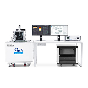
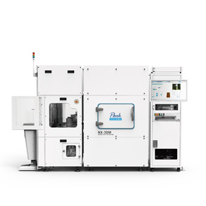
Park NX-Wafer原子力显微镜提供精准的形貌量测,可用来监控化学机械研磨平面化制程,检测因材料差异所造成异质材料间的凹陷(dishing)效应与浸蚀(errosion)效应。同时NX-Wafer还具有原子力形貌量测能力,可用以检测毫米横向尺度范围以及纳米级纵向尺度的高度变化。


9月17日,来自汉阳大学的Tae-gon Kim教授在使用Park NX-Wafer原子力显微镜基础上在大会上给以“Automated In-line AFM for Surface Profiling in CMP Applications”为主题的大会报告。
请下拉查看Prof. Tae-gon Kim大会报告的extended abstract.
---------------------------------
Automated In-line AFM for Surface Profiling in CMP Applications
Tae-Gon Kim1*, Sang-Joon Cho2, Ahjin Jo2, Byung-Woon Ahn2
1 Department of Smart Convergence Engineering, Hanyang University ERICA, Ansan, South Korea, 15588
2 Park Systems Corp, KANC 4F, Gwanggyo-ro 109 Suwon, South Korea 16229
*Corresponding e-mail: tgon@hanyang.ac.kr
Keywords: AFM, Profiling, In-line metrology
ABSTRACT – In advanced interconnect, CMP processes are becoming important and proper metrology solutions need to be introduced in order to fulfill the requirement of interconnect technology and their CMP processes. Automated in-line AFM with a sliding stage was demonstrated to show the capabilities of narrow trench measurement in large-scale profiling. Decoupled XY scanner and a sliding stage hybrid AFM system provides good measurement capabilities in dishing and erosion of narrow trench with wide range of scan distance. Therefore, in-line AFM with sliding stage could provide a non-destructive and direct metrology solution for CMP process developments of advanced interconnect.
INTRODUCTION
As devices are being scaled down to 7, 5 and 3 nm and the complexity of their architecture increases, the local and global flatness of wafer are becoming utmost important. Not only the flatness of layer and the erosion and dishing characteristics in narrow trench after CMP processes are critical to measure for better CMP process quality. Unfortunately, conventional metrology solution based on either optic or e-beam techniques does not fulfil the requirement of advanced CMP process control due to poor resolution in either vertical or lateral directions in large-scale area. It means that a metrology solution for better CMP process variation control requires a capability of narrow trench measurement in wide range distance and it should perform in non-destructive way.
In traditional, surface profilometry and ellipsometry are being used to measure height change and CMP nonuniformity, but height offset between device structure and measurement structure is always present due to the difference of pattern size and density. The offset needs to be evaluated by SEM or TEM, but those e-beam based techniques could also damage sample while measuring or preparing sample even though those techniques provide high resolution cross-section image. Therefore, it would be favourable to have a metrology solution, which could measure an atomic scale depth of a narrow trench with large-scale profiling. Even though conventional profilometry provides a quick step height measurement solution in large-scale, it is being used less and less in advanced CMP process due to the inaccessibility of narrow trench of the stylus probe. On the other hands, atomic force microscopy (AFM) utilizes a fine probe, which could access fine trench smaller than the trench size the stylus probe is not accessible. In this paper, we evaluated a fully automated in-line AFM system in terms of trench accessibility with a wide range of scan distance to provide a better CMP metrology solution in local and global height variation.
ATOMIC FORCE PROFILER
In order to achieve the higher resolution of AFM and the larger measurement range of surface profilers, AFM and long-range profiler hybrid system (Park Systems, NX-Wafer) was used. The AFM system is based on decoupled XY and Z scanner design to eliminate the cross-talk between the scanners and provide better positioning capabilities, which conventional tube based [1] AFM systems could not achieve.
Measurements were done in non-contact mode, which is performed by oscillating the AFM cantilever at its resonance frequency and modulating the oscillation amplitude by changing the position of the tip such that the tip-sample interaction remains in the attractive regime [2]. The advanced in-line AFM system utilizes non-contact mode to improve data consistency and preserves tip lifetime.
SMALL SCALE PROFILING
The new scanner design, decoupled flexure guided XY scanner is moved by two pairs of stacked piezo actuator in two in-plane directions. The background out-of-plane motion (OPM) for the XY scanner is below 2 nm for 100x100 μm scanner range. The reduced background OPM of XY scanner allows surface profiling of up to 100 μm ranges using only the XY scanner. Figure 1 shows an example of small-scale profiling using only the AFM XY scanner.
Figure 1 Small-scale profiling using AFM decoupled XY scanner. The scan range is 100 μm and the step height is 160 nm. The insert shows a magnified section of the same profile.
LONG-SCALE PROFILING
Long range profiling capability has become possible by the additional of a sliding stage underneath the XY scanner in the system. The sliding stage provides surface profiling using decoupled Z scanner over longer mm-scale ranges up to 50 mm comparing to μm-scale range for AFM scanner. Figure 2 shows a result of the long-scale profiling using the AFM system. Upper image is the optical sample image where the profile obtained and the profiling range is 30 mm and the step height is 400 nm. The profile data shows topography changes across the profiling range of 30 mm with minimum OPM.
One of the applications of long-scale profiling is monitoring dishing and erosion in CMP process. Dishing and erosion could differ at different locations due to different polishing rate caused by differences of local loading pressure, pattern density, so on. CMP metrology solution should provide the information of nano-scale dishing and erosion in long-scale profiling. Figure 3 shows nano-scale profile difference at the center, middle and edge of wafer. It shows high wafer non-uniformity across the wafer, which is a big difference in dishing and erosion from center to edge. It also shows that AFM with sliding stage provides a high-resolution profile with small noise.
Figure 2 Long-scale profiling using AFP scanner. Upper image is the optical sample image where the profile obtained. The range is 30 mm and the step height is 400 nm. The inset (down) shows an AFM image of the specific part of the profile.
Figure 3 Comparison of erosion and dishing profiles measured at center, middle and edge of wafer after CMP. Upper image is the optical sample image where the profile obtained.
NARROW Trench Measurement
In advance interconnect technology, beyond N10, the metal pitch dramatically decreases and Cu might need to be replaced by Co, Mo and Ru, which have lower resistivity at smaller CD than Cu. It means that CMP metrology for advanced interconnect technology should provide a solution of depth measurement at narrow trench, smaller than 50 nm [3]. In order to provide the narrow trench measurement capabilities, the narrow trench mode has been developed and introduced in the AFM system. Figure 4 shows comparison of trench measurement capabilities between the non-contact mode and the narrow trench mode at various trench width. The narrow trench mode shows good measurement capabilities at a trench with of 21 nm and a probe could reach a depth of 30 nm at a trench width of 16 nm.
Figure 4 Comparison of trench measurement capabilities between non-contact mode and narrow trench mode at various trench width.
Conclusions
Automated AFM with a sliding stage provides several capabilities of the dishing and erosion measurement in the narrow trench after CMP processes for advanced interconnect technologies. Unique design of decoupled XY and Z scanner allows to measure good profile information with ultra-low noise and minimum out-of-plane motion. Automated AFM metrology is suitable solution for in-line monitoring of CMP development and their performance.
REFERENCES
T. Cunningham, et al., (2000) "Atomic force profilometry and long scan atomic force microscopy: new techniques for characterisation of surfaces," Surface Engineering, 16(4) 295-298.
A. Zandiatashbar, et al., (2015) “Automatic defect review for EUV photomask reticles by atomic force microscope” Proc. SPIE 9635, Photomask Technology, 23 October, 2015, 96351A.
A. Sekiguchi, (2016) “Patterning technology for N5”, IEDM Short Course, 4 December, 2016.
更多![]()
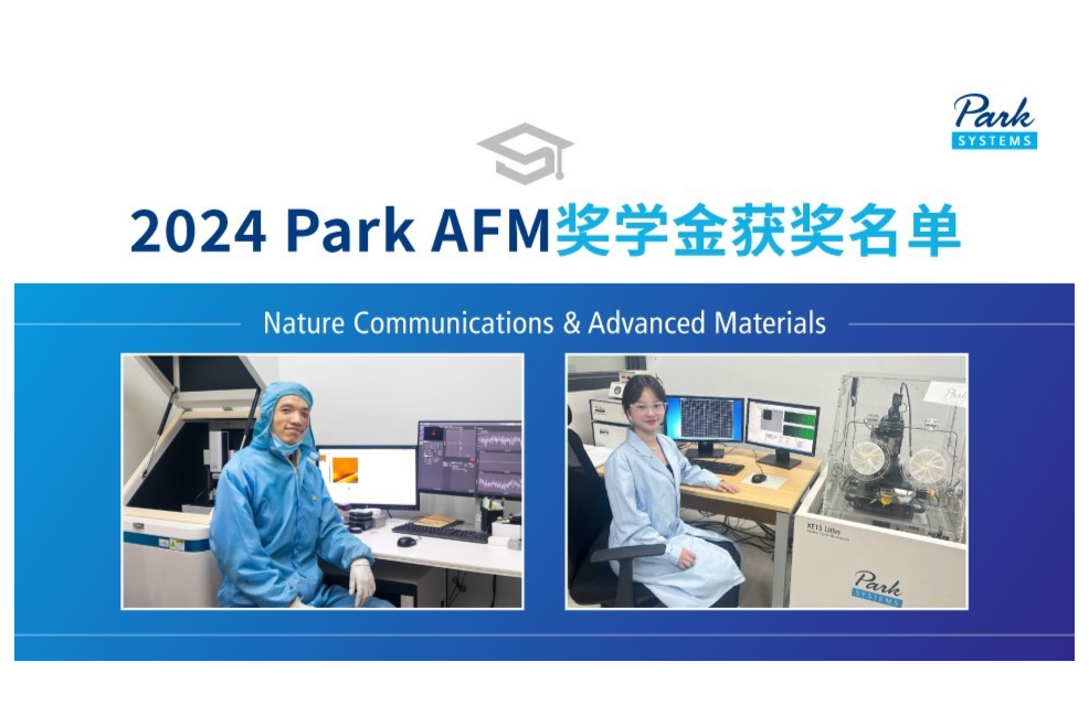
最新!2024 Park AFM第一批奖学金获奖名单公布
厂商
2024.05.14
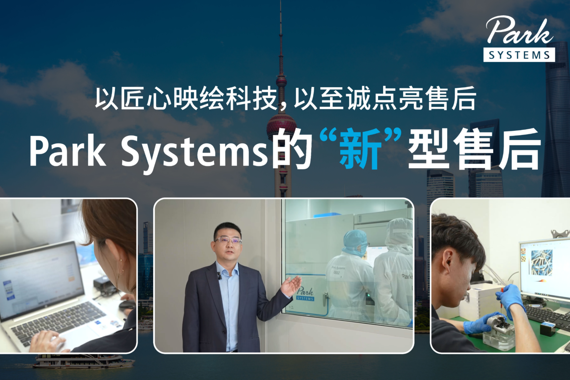
以匠心映绘科技,以至诚点亮售后——Park Systems的“新”型售后
厂商
2024.04.23

积极响应国家利好政策: Park Systems 支持设备更新,助力节能提效
厂商
2024.04.01
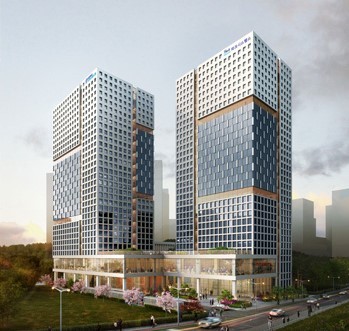
里程碑!投资642亿韩元,Park Systems新总部建设项目开工
厂商
2023.09.27
公司名称: Park帕克原子力显微镜
公司地址: 北京市海淀区彩和坊路天创科技大厦518室 联系人: 张菲 邮编: 100080 联系电话: 400-878-6829
仪器信息网APP

展位手机站