搜全站
搜展位

牛津仪器科技(上海)有限公司
 关注
关注
已关注
白金23年

![]() 已认证
已认证
粉丝量 0

400-860-2711
仪器信息网认证电话,请放心拨打
解决方案

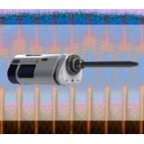
Mapping Semiconductor Devices in the SEM
应用领域
半导体检测样品
其他检测项目
元素构成分析Introduction
Application Note
As semiconductor devices continue to decrease in size to improve performance and take advantage of
advances in fabrication techniques, there is a need to analyse both their structure and chemistry at ever
increasing resolution. Typically this requires the use of TEM for metrology and failure analysis. Using ultrahigh
resolution FEG-SEM, low kV imaging and the new X-Max® Extreme EDS detector we demonstrate
the ability to retain some of this high resolution analysis in the SEM. This allows for better targeting of
resources and increased throughput of analysis.
共1台
Simultaneous EDS and EELS Analysis in the TEM
应用领域
半导体检测样品
其他检测项目
完全表征Introduction
In Transmission Electron Microscopy (TEM) there are two ‘go to’ techniques for elemental analysis: Energy
Dispersive X-ray Spectroscopy, (EDS), and Electron Energy Loss Spectroscopy, (EELS).
EDS is a mature technique that can be used for most specimens. The intensity of generated X-rays
is proportional to the mass thickness of the sample. However, this can become a limitation for very
thin specimens or those comprising light elements. On the other hand, EELS is more suitable for thin
samples where the thickness is less than the inelastic mean free path of electrons in the material. EELS
does, however, give high signal to noise for light elements. Simultaneous acquisition of both signals is a
powerful tool for materials analysis.
共1台
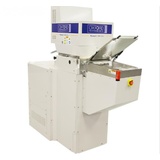
等离子体原子层刻蚀实现无损伤刻蚀
应用领域
半导体检测样品
其他检测项目
原子层蚀刻提供等离子体原子层刻蚀实现无损伤刻蚀。原子层蚀刻(ALE)是一种技术允许每次精确除去一个原子层,是使用常规刻蚀无法达到的控制水平。 牛津仪器的设备和工艺已通过充分验证,正常运转时间可达90%以上,一旦设备安装完毕,可立即投入使用。PlasmaPro 100系列市场应用广,包括但不限于: MEMS和传感器、光电子、分立元器件和纳米技术。它具有足够的灵活性,可用于研究和开发,通过打造质量满足生产需求。
共1台
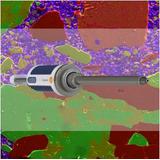
NA-EDS-Extreme-半导体
应用领域
半导体检测样品
其他检测项目
结构Introduction
Application Note
As semiconductor devices continue to decrease in size to improve performance and take advantage of
advances in fabrication techniques, there is a need to analyse both their structure and chemistry at ever
increasing resolution. Typically this requires the use of TEM for metrology and failure analysis. Using ultrahigh
resolution FEG-SEM, low kV imaging and the new X-Max® Extreme EDS detector we demonstrate
the ability to retain some of this high resolution analysis in the SEM. This allows for better targeting of
resources and increased throughput of analysis.
共4台
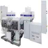
NA-EDS for TEM-半导体
应用领域
半导体检测样品
其他检测项目
局部结构和元素组成Development and testing of semiconductor devices requires extensive knowledge of local structure and elemental
composition. With feature sizes of <5 nm, it is often necessary to perform imaging and EDS analysis in a S / TEM.
Once in the TEM, there are still many difficulties to be overcome to acquire accurate elemental maps. Elemental
analysis of semiconductors is typically difficult due to strong overlaps of X-ray lines between commonly used elements
and low concentrations of dopants. Not only are concentrations of dopants small but their X-ray lines often overlap
with other materials used in semiconductor processing. This brief shows how AZtecTEM solves these overlaps to
achieve an accurate elemental analysis.
TEM Semiconductor Mapping in the TEM
Solving peak overlaps in real-time
Application Brief
共3台
联系方式:
公司名称: 牛津仪器科技(上海)有限公司
公司地址: 上海市徐汇区虹漕路461号虹钦园60号楼1楼 联系人: 牛津仪器 邮编: 200233 联系电话: 400-860-2711
主营产品:
友情链接:
仪器信息网APP

展位手机站