
 关注
关注
已关注

![]() 已认证
已认证
粉丝量 0

400-860-2711
仪器信息网认证电话,请放心拨打
核心参数
产地类别: 进口
CCD相机分辨率: 1244×1024
极限速度: 870Hz
空间分辨率: 2nm
角分辨率: 优于0.05°
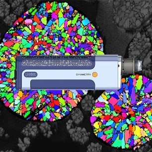
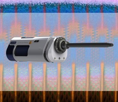
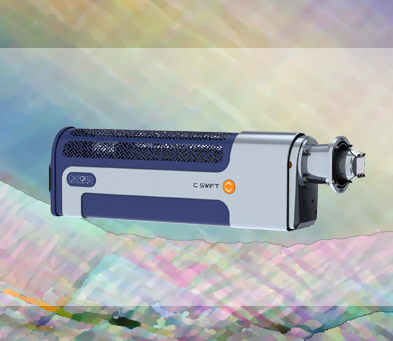
C-Swift是CMOS探测器家族的新成员,专为常规材料分析和快速样品表征而设计。
C-Swift继承了Symmetry的许多优点,包括为EBSD专门定制CMOS传感器。这些优点使得C-Swift也成为一种开创性的EBSD探测器。
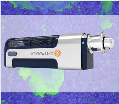
C-Swift是一个先进、高速EBSD探测器。与Symmetry探测器一样,C-Swift使用定制的CMOS传感器来实现高速和高灵敏度,以确保即使在更具挑战性的材料上也能获得高质量的结果。
C-Swift速度高达1000pps,同时可获得高质量的花样分辨率(156x128像素)。这相当于基于CCD的探测器以相似速度运行时所采集花样像素数的4倍,确保所有类型样品的可靠标定和高命中率。无失真光学系统与AZtec软件中强大的标定算法结合,使C-Swift能够提供优于0.05°的高角度精度。对于需要更高质量花样的应用, C-Swift可以以高达250pps的速度采集622x512像素的花样,使其成为复杂的多相样品和精细的相分析的理想选择。
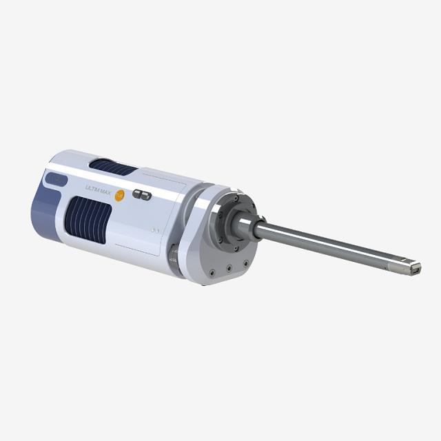
这是专为快速、有效的样品表征而设计的探测器。系统的每个组件,从独特的接近传感器到可选的集成前置探测器,都经过设计, 旨在更大限度地提高性能和易用性, 并使EBSD成为每个实验室的标准工具。
确保1000 点/秒的标定速度
在250点/秒速度下,采集622x512像素的EBSD花样
对低能量和低束流分析具有非常高的灵敏度
无失真图像
当速度是关键时,C-Swift探测器达到了一个新标准:
仅需要12nA的电子束流,就能保证1000pps的标定速度
高速下的156x128像素的花样分辨率——同等速度下快速CCD探测器的4倍
全分辨率花样(622x512像素)——精细的相分析和形变分析的理想选择
低失真光学系统, 确保角度精度优于0.05°
优化的高灵敏度荧光屏, 确保低剂量和低束流能量下的高质量的花样——实现更大的空间分辨率
即使在快速下也能实现无缝的EDS集成
波纹管SEM接口,保持SEM真空完整性
独特的接近传感器——在可能发生的碰撞发生之前自动将探测器移动到安全位置
简单直观的探测器设置,确保每次都能获得良好的效果
五个集成的前置探测器, 提供全彩色通道衬度图像和原子序数衬度图像
牛津仪器EBSD系统C-Swift的工作原理介绍
EBSD系统C-Swift的使用方法?
牛津仪器C-Swift多少钱一台?
EBSD系统C-Swift可以检测什么?
EBSD系统C-Swift使用的注意事项?
牛津仪器C-Swift的说明书有吗?
牛津仪器EBSD系统C-Swift的操作规程有吗?
牛津仪器EBSD系统C-Swift报价含票含运吗?
牛津仪器C-Swift有现货吗?
更多![]()


更多![]()
NA-EDS-Extreme-半导体
Introduction Application Note As semiconductor devices continue to decrease in size to improve performance and take advantage of advances in fabrication techniques, there is a need to analyse both their structure and chemistry at ever increasing resolution. Typically this requires the use of TEM for metrology and failure analysis. Using ultrahigh resolution FEG-SEM, low kV imaging and the new X-Max® Extreme EDS detector we demonstrate the ability to retain some of this high resolution analysis in the SEM. This allows for better targeting of resources and increased throughput of analysis.
半导体
2018/01/08
NA-EDS for TEM-半导体
Development and testing of semiconductor devices requires extensive knowledge of local structure and elemental composition. With feature sizes of <5 nm, it is often necessary to perform imaging and EDS analysis in a S / TEM. Once in the TEM, there are still many difficulties to be overcome to acquire accurate elemental maps. Elemental analysis of semiconductors is typically difficult due to strong overlaps of X-ray lines between commonly used elements and low concentrations of dopants. Not only are concentrations of dopants small but their X-ray lines often overlap with other materials used in semiconductor processing. This brief shows how AZtecTEM solves these overlaps to achieve an accurate elemental analysis. TEM Semiconductor Mapping in the TEM Solving peak overlaps in real-time Application Brief
半导体
2018/01/08
企业名称
牛津仪器科技(上海)有限公司
企业信息已认证
企业类型
信用代码
310000400824735
成立日期
2017-03-29
注册资本
50
经营范围
精密仪器和设备的技术开发、技术服务、技术转让和技术咨询,精密仪器和设备的批发、进出口,佣金代理(拍卖除外),并提供维修服务和相关配套服务。【依法须经批准的项目,经相关部门批准后方可开展经营活动】
牛津仪器科技(上海)有限公司
公司地址
上海市徐汇区虹漕路461号虹钦园60号楼1楼
客服电话
公司名称: 牛津仪器科技(上海)有限公司
公司地址: 上海市徐汇区虹漕路461号虹钦园60号楼1楼 联系人: 牛津仪器 邮编: 200233 联系电话: 400-860-2711
仪器信息网APP

展位手机站