视频号

抖音号

哔哩哔哩号

前沿资讯手机看

热分析&电镜&表面分析,分享最新国内外仪器技术成果进展


分享到微信朋友圈
打开微信,点击底部的“发现”,
使用“扫一扫”即可将网页分享到朋友圈。
2022年7月26-29日,仪器信息网(www.instrument.com.cn) 与中国电子显微镜学会(www.china-em.cn)将联合主办“第八届电子显微学网络会议(iCEM 2022)”。
iCEM 2022将围绕当下电子显微学研究及应用热点,邀请业界知名电子显微学专家线上分享精彩报告。分设:电子显微学技术及应用进展、原位电子显微学技术及应用、电子显微学技术在先进材料中的应用、电镜实验操作技术及经验分享、电子显微学技术在材料领域应用、电子显微学技术在生命科学领域应用6个主题专场,诚邀业界人士报名参会。
主办单位
仪器信息网、中国电子显微镜学会
参会方式
本次会议免费参会,参会报名请点击会议官网:
https://www.instrument.com.cn/webinar/meetings/iCEM2022

或扫描二维码报名
以下为“先进电子显微学技术及应用”专场预告
(注:最终日程以会议官网发布为准)
专场三:先进电子显微学技术及应用 (7月27日上午) 专场主持人:王立华 北京工业大学 教授 |
||
时间 |
报告题目 |
演讲嘉宾 |
08:30--09:00 |
基于叠层电子衍射的断层扫描三维成像技术(Electron ptychographic computed tomography) |
王鹏(南京大学 教授) |
09:00--09:30 |
跨尺度锂电池研究 |
黄建宇(燕山大学 教授) |
09:30--10:00 |
国仪量子电镜研发最新进展及应用 |
尹相斐(国仪量子(合肥)技术有限公司 应用工程师) |
10:00--10:30 |
The ESEM as In Situ Platform for the Study of Gas-Solid Interactions |
王竹君(上海科技大学) |
10:30--11:00 |
TESCAN双束电镜的最新技术进展 |
余妍(TESCAN CHINA 资深应用工程师) |
11:00--11:30 |
聚束科技NavigatorSEM-100的技术突破及应用 |
李帅(聚束科技(北京)有限公司 总经理) |
11:30--12:00 |
晶界塑性变形原子层次机理的原位研究 |
王立华(北京工业大学 教授) |
12:00--12:30 |
3D Electron Diffraction Methods for Crystal Structure Determination |
徐弘毅(瑞典斯德哥尔摩大学 研究员) |
嘉宾简介及报告摘要
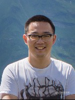
华威大学教授 王鹏
【个人简介】
王鹏,教授,博士导师,长期从事功能材料结构与缺陷的微观表征和基于大数据的计算机高分辨成像学的研究工作。2012年回国到南京大学任教,组建了南大亚原子分辨电镜中心。近五年发表论文100篇,其中第一作者/通讯作者论文40余篇,包括1篇Nature、2篇Nature Electronics、3篇Nature Communications、1篇Physical Review Letters、2篇Advanced Materials。申请及获得多项发明专利,包括3件国际专利申请,12件中国专利(其中10件授权)。H-index 为36。科技部“973”首席科学家,主持和参与国际合作项目以及其他国家和省部级项目多项,担任中国晶体学、电镜、真空等学会理事。
报告题目:基于叠层电子衍射的断层扫描三维成像技术(Electron ptychographic computed tomography)
【摘要】结合高速相机4DSTEM衍射大数据,基于计算机算法的Ptychography “无透镜”叠层电子衍射技术不受磁透镜固有像差的限制,可以获得超高分辨率,高相位衬度,轻元素敏感,低噪声,低辐照损伤的二维到三维原子结构信息,有望应用于含有轻元素、辐照极易损伤材料的高分辨结构表征,在能源存储材料和结构生物大分子结构解析领域有潜在广泛应用前景。
燕山大学/湘潭大学教授 黄建宇
【个人简介】
黄建宇,燕山大学和湘潭大学教授,博士生导师。博士毕业于中科院金属研究所;此后于日本国家无机材料研究所、日本大阪大学、美国洛斯阿拉莫斯国家实验室、波斯顿学院、桑迪亚国家实验室先后任职。一直以来以电子显微镜为主要研究手段,从事纳米力学与能源科学研究工作20多年。在电池研究领域取得了系列原创性的研究成果,建立了多种纳米力学和能源材料透射电镜-探针显微镜(TEM-SPM)的原位定量测量技术,在国际上率先制造出可在高真空度电镜中工作的锂电池,发明了在原子尺度上实时观察锂离子电池充放电过程的新技术,形成了原位纳米尺度电化学研究新领域,为锂离子电池研究提供了有效的技术手段。研究成果在《Science》、《Physical Review Letters》、《Nature Nanotechnology》、《Nature Communications》、《Nature Methods》、《PNAS》、《Nano Letters》等杂志上发表,共发表论文270余篇,h因子90,总引用次数近28000次,在各种专业学术会议上发表特邀报告100多次。
报告题目:跨尺度锂电池研究
【摘要】高能量密度、长循环和高安全性锂电池的制备涉及到材料制备/表征,极片涂覆和电池组装等多尺度结构优化。因此电池设计是一个多尺度问题,任何一个环节出现问题都会导致电池劣化和失效。因此发展跨尺度锂电池表征技术尤为重要。近年来本研究组一直从事多尺度锂电池表征技术开发。在宏观层面,设计出原位光学表征技术,成功地在宏观尺度揭示固态电池锂枝晶生长和传输机制。在介观层面,开发出在FIB-SEM里面微米尺度电池,发现硫化物电解质电化学-力学耦合失效尺寸效应。在微观领域,结合透射电镜和探针显微镜(TEM-STM),实现了纳米材料的微观结构和性能的同步测量。利用TEM-STM平台,首次在电镜中构建了纳米电池,实现了对电化学反应的实时原位观测,开创了纳米电化学新领域。结合微机电加热系统,原子力显微镜和球差矫正环境电镜,利用TEM-STM平台可以实现温度、压力和气氛多场耦合条件下的原位电化学测量。本报告将介绍应用原位光学、FIB-SEM和TEM-STM平台在锂电池研究领域的最新研究成果。在纳米电池领域,发现锂嵌入硅导致粉化的尺寸效应。测定了锂、钠枝晶的力学性能,发现纳米锂、钠枝晶的强度比相应的体材强度高出200多倍。实现了锂枝晶的力-电耦合精准测量,揭示锂枝晶刺穿固态电解质机理。利用球差矫正环境电镜,实现了气体电池的原位测量。这些基础研究为开发高能量密度、高功率密度和长循环寿命锂电池提供了坚实的科学基础和技术路径。
上海科技大学教授 王竹君
【个人简介】
主要从事开发新型电子束扫描成像技术及其在表面科学与催化科学中的应用研究,拥有10年以上的真空差分设计与电子显微镜扫描成像技术开发实绩。基于自主发展的原位观测方法,在金属催化剂表面上低维纳米材料演化行为与机理、表界面化学振荡等领域取得了系列创新性研究成果。开创了在极端环境下(高温、近常压小分子与腐蚀性气氛)具有表面原子级敏感的实空间实时成像表征方案;精确测量了化学气相沉积过程中二维材料的堆垛次序、层间作用力、生长与拼接行为等可精确操控材料结构性质的关键参数;揭示了金属表面催化反应进程中的产物转化率与时空斑(spatiotemporal patterns)行为之间的构效关系;以扫描电子束成像手段为桥梁,开发了表界面的多重多尺度原位观测手段,并尝试弥合了长期困扰表面实验科学中的三大鸿沟问题。
报告题目:The ESEM as In Situ Platform for the Study of Gas-Solid Interactions
【摘要】In order to understand the working principle of functional materials they should, at one point, be studied in their working state. In view of electron microscopy, atomic motion and chemical dynamics can be observed by in situ TEM. However, size constraints and the requirement of electron beam transparency impose substantial limitations with respect to dimension, complexity, and preparation of a specimen. Furthermore, atomistic details can only be resolved under conditions where atomic scale dynamics are slow compared to the temporal resolution of the detection system. In the case of gas-solid interactions, in situ TEM observations are therefore often performed at the reduced chemical potential of the reactive gas phase. Due to the strong focus on ultimate spatial resolution, the potential of environmental scanning electron microscopy (ESEM) as a flexible tool for in situ studies in the field of material science has recently been overlooked. In situ experiments performed in the ESEM can be used to complement localized information that is obtained by in situ TEM. Instead of atomistic details, it reveals the complexity of hierarchical multi-scale processes in which collective movements of a large number of atoms are involved. Thus, effects related to heat and mass transport are accessible. Compared to the TEM, the ESEM imposes far fewer restrictions with respect to available space and dimensions of the sample. This opens up the possibility to bridge the “materials gap” between simplified models- and complex real-world systems. Similarly, the focus on collective dynamics allow observations at the higher chemical potential of the reactive species and thus, a closing of the so-called “pressure gap”. Another important aspect is the reduced areal dose rate and lower kinetic energy of the beam electrons in ESEM. Contributions and extent of various beam-induced processes are different and, in most cases, less severe than in the TEM. Furthermore, the ESEM allows fast and efficient screening of the parameter field and facilitates more efficient use of the in situ TEM set-up. In order to obtain a unique platform for in situ studies of gas-solid interactions under a controlled atmosphere, we have equipped a commercial ESEM with a home-built gas-feeding station, a heating stage, and a mass spectrometer. For topography and 3D imaging of surface dynamics at temperatures of up to 1000 °C, a newly developed four-quadrant BSE detector was implemented. In addition, a detector for electron beam absorbed current (EBAC) was installed in order to complement the large-field detector with a signal that is independent of gas composition and pressure. It will be shown how the use of this instrument allows to study the emergence of catalytic function in the interplay between a gas phase and a metal catalyst. Dynamics of metal catalysts under redox conditions will be presented as well as the ability to study vapour-liquid-solid growth of 2D ribbon. Due to the high sensitivity of the SE signal, it is even possible to study metal catalysed chemical vapour deposition of graphene at 1000 °C. Finally, it will be demonstrated that contrast variations due to different molecular species on the surface of platinum during catalytic NO2 hydrogenation can be detected.
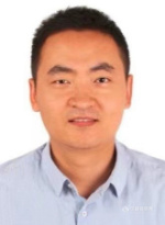
北京工业大学教授 王立华
【个人简介】
王立华,研究员,博士生导师,国家优秀青年基金获得者。2012年获得北京工业大学博士学位。2015-2017年,获得澳大利亚政府资助(Discovery Early Career Researcher Award),在昆士兰大学(全球排名前50)从事博士后研究工作。入选北京市卓越青年科学家、霍英东青年教师基金等人才计划。长期从事“原子尺度下材料力学行为的原位实验研究”,发表论文60余篇,其中包括自然子刊Nat. Commun. 4篇,Phys. Rev. Lett.1篇、Nano Lett. 4篇,Acta Mater.3篇,Appl. Phys. Lett.5篇等,被国际同行引用3000余次。主要成果获得2016年北京市科学技术奖一等奖,获北京市优博论文奖、郭可信优秀青年学子奖等。承担国家重点研发计划子课题、国家自然科学基金优秀青年基金、面上项目等多项国家及省部级项目。第一或通讯作者发表主要论文:1. Deli Kong et al., Nano Letters 19, 292 (2019).2. L. H. Wang et al., Physical Review Letters, 105, 135501 (2010)3. L. H. Wang et al., Nature Communications, 4, 2413 (2013)4. L. H. Wang et al., Nature Communications, 5, 4402 (2014)5. L. H. Wang et al., Nature Communications, 8, 2421 (2017)6. L. H. Wang et al., Nat. Commun. 11, 1167 (2020).7. L. H. Wang et al., Nano Letters, 17, 4733 (2017).8. L. H. Wang et al., Nano Letters. 11, 2382 (2011).9. L. H. Wang et al., ACS Nano, 2017, 11, 1250010. Shiduo Sun et al., ACS Nano, 13, 8708 (2019).
报告题目:晶界塑性变形原子层次机理的原位研究
【摘要】晶体变形过程中缺陷的形核及演化是组成这些缺陷的原子集体响应的动态过程。由于原有的原位实验技术分辨率长期局限于纳米尺度,导致人们对晶界变形的原子层次机理的认知强烈依赖于理论模型及计算机模拟,亟需原子层次原位实验证据澄清晶界塑性变形机制。本次报告主要介绍近年来团队在晶界变形机制研究的进展。主要是利用原创的实验技术,实现了多晶体系中晶界滑移、晶界原子扩散的原子层次动态观察。揭示出晶界滑移是通过晶界处原子相对滑移与原子短程扩散相互协调实现。研究晶界原子阵列合并消失、分裂出新原子阵列、原子迁移并插入晶体内部等多种新型的扩散机制。通过原位观察,发现晶界的产生及晶粒旋转的机制。
瑞典斯德哥尔摩大学研究员 徐弘毅
【个人简介】
After completing a Bachelor of Engineering (Mechatronics) degree at the University of Queensland (UQ), Hongyi went on to pursue a PhD degree in materials engineering, specialized in electron microscopy and semiconductor nano-materials. The Australian Government sponsored his PhD study through the Australian Postgraduate Award program. He obtained his PhD degree at UQ in Dec 2013, and received the Dean’s accommodation for academic excellence as well as the best thesis of the year award from the School of Mechanical and Mining Engineering. In Feb. 2014, Hongyi started his postdoc fellowship (Wenner-Gren Foundation postdoc award) in Prof. Xiaodong Zou’s group at Stockholm University. In 2015, he initiated the development of MicroED (3D electron diffraction technique for studying biomolecules) at Zou’s group. Hongyi became a principle investigator in 2018 to further develop and apply electron crystallography methods for studying structures of biomolecules. Recently, Hongyi and colleagues solved the first two previously unknown protein structures using MicroED. They have also shown that it is possible to reveal protein inhibitor binding by MicroED. Hongyi is now working as a researcher/principle investigator at Stockholm University.
报告题目:3D Electron Diffraction Methods for Crystal Structure Determination
【摘要】Knowing the 3D atomic structures of materials or biomolecules is crucial for understanding their functions. X-ray diffraction is currently the most important technique for determination of 3D atomic structures, but requires large crystals which are often difficult to obtain. Electrons, similar to X-rays and neutrons, are powerful source for diffraction experiments. Due to the strong interactions between electrons and matter, crystals that are considered as powder in X-ray crystallography can be treated as single crystals by 3D electron diffraction methods. This enables structure determination of materials and organic molecules from micron- to nanometer-sized 3D crystals that are too small for conventional X-ray diffraction. Furthermore, by taking the advantages of the unique properties of electron scattering, it is possible to determine the charge states of atoms/ions and the absolute structure of chiral crystals. Over the past decades, a number of 3D ED methods have been developed for structure determination. At the early stages of 3D ED method development, tilting of the crystal was done manually, while diffraction patterns were collected on negative film. It could take years before sufficient data were obtained and processed in order to determine the crystal structure. The computerization of TEMs and the development of CCD detectors allowed software to be developed that can semi-automatically collect 3D ED data in less than an hour. Thanks to the recent advancement in CMOS and hybrid detector technology, it is now feasible to collect diffraction data in movie mode while continuously rotating the crystal (continuous rotation election diffraction, cRED, also known as MicroED in structural biology). Benefiting from these technological advances, structure determination can now be accomplished within a few hours. Recently, fully automated serial rotation electron diffraction data collection and processing has been realized by our group. By using 3D ED / MicroED methods, we have solved more than 200 novel crystal structures of small inorganic compounds (including zeolite, MOF, COF and minerals) and biomolecules (pharmaceuticals, small organic molecules, peptides and proteins) in the past 7 years. Recently, we have solved two novel protein structures with 3D ED/MicroED and shown that it is feasible to use MicroED for structure based drug discovery. We aim to further improve these methods, develop new methods and more importantly spread them to labs around the world.
国仪量子(合肥)技术有限公司应用工程师 尹相斐
【个人简介】
尹相斐,国仪量子电镜事业部SEM应用工程师,有多年显微成像分析经验。2021年硕士毕业于南京大学化学化工学院,目前从事国仪量子电子显微镜相关的显微分析应用开发与技术支持工作,已为近百家客户提供了DEMO演示和应用培训,竭诚为客户创造价值。
报告题目:国仪量子电镜研发最新进展及应用
【摘要】国仪量子在显微成像领域有近20年的技术积累,于2018年发布了第一台商用扫描电镜,经过不断地优化升级,目前国仪量子的SEM3200型钨灯丝扫描电镜和SEM5000型场发射扫描电镜已具有出色的成像质量、丰富的扩展性、完善的自动功能和便捷的交互操作,能够帮助用户快速完成高分辨样品拍摄和显微分析,助力学术和工业用户在新能源、微电子、材料科学、生物医疗等领域的新材料研发和工艺优化。
TESCAN CHINA资深应用工程师 余妍
【个人简介】
材料学硕士,毕业于华侨大学。2019年加入TESCAN CHINA应用部,负责扫描电镜售前DEMO和售后技术服务工作。2011年开始负责FIB-SEM 售前技术交流、制样演示和售后技术服务工作。熟悉SEM和FIB在材料科学、半导体科学等领域的应用。
报告题目:TESCAN双束电镜的最新技术进展
【摘要】 TESCAN双束电镜结合了高精度的FIB镜筒和超高分辨的SEM镜筒,同时拥有最佳离子束铣削能力和超高分辨率成像能力。镓离子FIB可以对10nm以下支撑的半导体器件进行高效、定点制备TEM样品;氙气等离子体FIB可以轻松应对宽达1mm的大面积截面加工。
聚束科技(北京)有限公司总经理 李帅
【个人简介】
李帅,男,聚束科技(北京)有限公司总经理、联合创始人。2008年在ASML-HMI任职并从事于半导体工业用扫描电镜的开发。2015年共同创立聚束科技(北京)有限公司,公司推出的视频级成像能力的高通量扫描电镜NavigatorSEM-100,上市后荣获了众多国内外大奖。长期从事电子光学和电子显微镜技术相关研究,获得国内外专利40余篇。
报告题目:聚束科技NavigatorSEM-100的技术突破及应用
【摘要】聚束科技独立研发并拥有自主知识产权的NavigatorSEM-100高通量(场发射)扫描电子显微镜,通过对成像技术、运动平台、电路控制及智能算法的系统化创新设计,实现了全球最高通量成像,成像速度可达到传统电镜的数十倍以上。其全部采用直接电子探测器的技术方案,成功克服了传统SEM技术在速度、精度和样品损伤等方面的局限性,颠覆性地将扫描电镜从传统意义上的纳米“照相机”提升为纳米“摄像机”。
[来源:仪器信息网] 未经授权不得转载

直播预告!iCEM 2022之原位电子显微学技术及应用专场篇
2022.07.19
2024.07.29
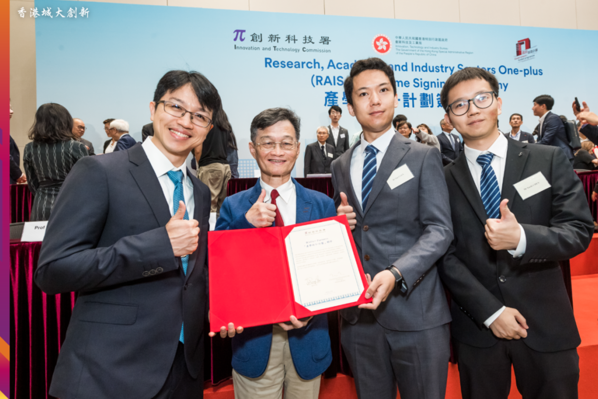
迈向量子电子显微镜!香港城大研发小型“脉冲空心锥扫描与透射一体化电子显微镜”
2024.07.26

2024.07.04

2024.06.19

2024.06.19
品牌合作伙伴


版权与免责声明:
① 凡本网注明"来源:仪器信息网"的所有作品,版权均属于仪器信息网,未经本网授权不得转载、摘编或利用其它方式使用。已获本网授权的作品,应在授权范围内使用,并注明"来源:仪器信息网"。违者本网将追究相关法律责任。
② 本网凡注明"来源:xxx(非本网)"的作品,均转载自其它媒体,转载目的在于传递更多信息,并不代表本网赞同其观点和对其真实性负责,且不承担此类作品侵权行为的直接责任及连带责任。如其他媒体、网站或个人从本网下载使用,必须保留本网注明的"稿件来源",并自负版权等法律责任。
③ 如涉及作品内容、版权等问题,请在作品发表之日起两周内与本网联系,否则视为默认仪器信息网有权转载。
![]() 谢谢您的赞赏,您的鼓励是我前进的动力~
谢谢您的赞赏,您的鼓励是我前进的动力~
打赏失败了~
评论成功+4积分
评论成功,积分获取达到限制
![]() 投票成功~
投票成功~
投票失败了~