 关注
关注
已关注

![]() 已认证
已认证
粉丝量 0
400-860-5168转4452
仪器信息网认证电话,请放心拨打
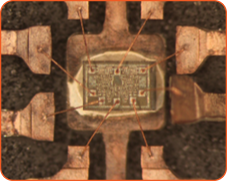
Protecting Those Sensitive Copper Wires.
It just got easier.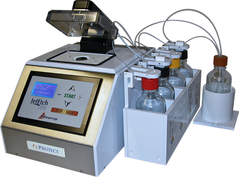
With the price of gold at an all-time high, a current trend in the manufacturing of integrated circuits is the shift from gold to copper bond wires. With this shift, the failure analyst of these processors is now challenged to successfully attain package decapsulation by use of traditional methods.
主要特征(Features):
The Old Methods.
Historically, one would use an automated chemical decapsulation system to etch samples with copper wires — with minimal success. Even with a low-temperature nitric and sulfuric acid mixture, and even in combination with laser pre-opening, this process works to an extent, but is largely unreliable. When faced with a limited number of field failures, which is a common scenario in a failure analysis laboratory setting, less reliable processes can’t be counted on to deliver satisfactory failure analysis and visual inspection results.
The Solution.
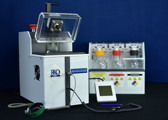
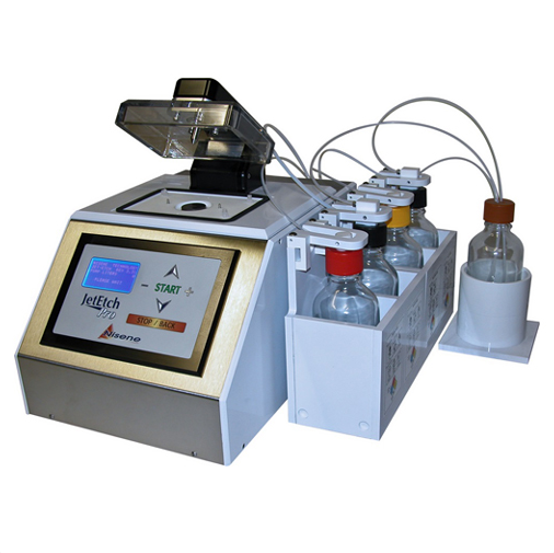
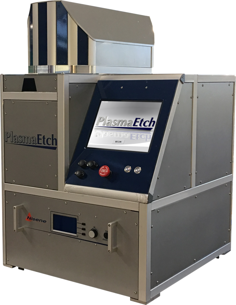
To support manufacturers in making this shift so that failure analysis can still be performed on their most advanced and cutting edge products which now use copper wire bonding, Nisene Technology Group has developed a version of its new JetEtch Pro decapsulation system that is specifically designed to handle the processing of this sensitive material: the JetEtch Pro CuProtect — the latest in a series of innovative solutions for the failure analysis industry from Nisene.
The Process.
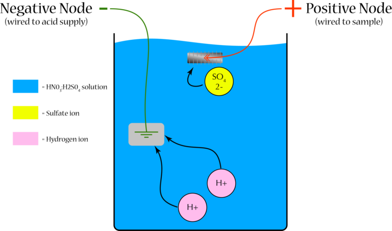 Using a proprietary and patented process, the JetEtch Pro CuProtect applies a bias to the solution being pumped to the sample in the process chamber. This bias creates a condition in which negatively-charged sulfate ions are attracted and temporarily bond to the surface of the copper wire while the sample is being etched. This temporary sulfate ion coating protects the copper wires from corrosion while the sample undergoes the etching process.
The image to the right illustrates the operating principal behind the technique. Click on the image to open a larger version in a new window.
In less sophisticated systems relying solely on low temperature etching, positively-charged hydrogen ions are attracted to the copper wires, thereby making the wires susceptible to pitting, cracking, breaking, and many other undesirable anomalous artifacts that greatly affect or even squelch completely the ability to perform failure analysis after the etching process. The Nisene Technology Group CuProtect system solves this problem.
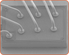
The Results.
As illustrated in the images below, the advanced bias application process yields results that are unmatched in the industry.
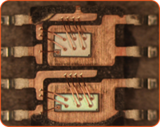
If you would like to see more examples of samples etched with the CuProtect, please contact us.
The Software.
“Surely something like this must be complicated to use and difficult to understand — right?” you ask. The answer to that is “of course not!” The system appears on the outside to be the same as the JetEtch Pro, but there is an added line in its decapsulation programming menu that allows the user to change the value of the applied bias. The range is 0 V (off or no bias) to 20.0 V, selectable in .1 V increments. The other differences between the CuProtect system and the JetEtch Pro — both in hardware and software — are hidden inside the system, so operating the CuProtect is exactly like JetEtch Pro and virtually transparent to a user. That is to say: learning curve is very small. There’s no need to learn anything new other than how much voltage to apply to your sample while it is etching.


One additional parameter line. Not much to learn here!
Nisene其他半导体检测仪JetetchPro-Cu的工作原理介绍
其他半导体检测仪JetetchPro-Cu的使用方法?
NiseneJetetchPro-Cu多少钱一台?
其他半导体检测仪JetetchPro-Cu可以检测什么?
其他半导体检测仪JetetchPro-Cu使用的注意事项?
NiseneJetetchPro-Cu的说明书有吗?
Nisene其他半导体检测仪JetetchPro-Cu的操作规程有吗?
Nisene其他半导体检测仪JetetchPro-Cu报价含票含运吗?
NiseneJetetchPro-Cu有现货吗?
更多![]()
企业名称
似空科学仪器(上海)有限公司
企业信息已认证
企业类型
信用代码
91310115MA1H9W0N9G
成立日期
2018-04-16
注册资本
500
经营范围
从事仪器仪表科技、计算机软硬件科技、工业自动化科技、智能科技、电子科技领域内的技术开发、技术咨询、技术服务、技术转让,仪器仪表、实验室设备、电子产品 、一般劳防用品、机电设备及配件、塑料制品、五金交电、日用百货、化工原料及产品(除危险化学品、监控化学品、民用爆炸物品、易制毒化学品)的销售,从事货物及技术的进出口业务。【依法须经批准的项目,经相关部门批准后方可开展经营活动】
似空科学仪器(上海)有限公司
公司地址
张江微电子港7号楼7楼
客服电话
公司名称: 似空科学仪器(上海)有限公司
公司地址: 张江微电子港7号楼7楼 联系人: 张经理 邮编: 201203 联系电话: 400-860-5168转4452
仪器信息网APP

展位手机站