
 关注
关注
已关注

![]() 已认证
已认证
粉丝量 0
400-860-5168转2024
仪器信息网认证电话,请放心拨打
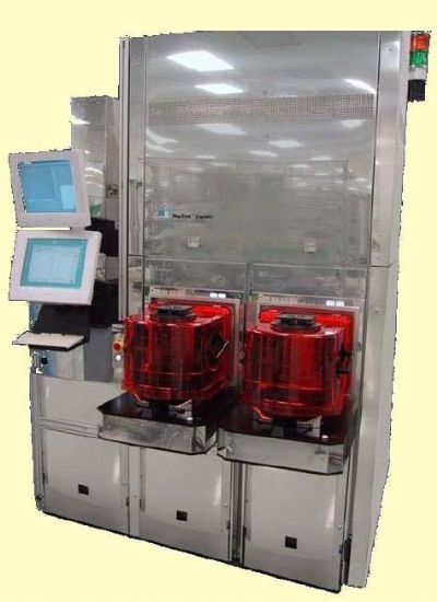
tSeries 300mm Sorters

300mm FOUP/FOSB carrier compatible·2 / 3 port inline or 4 / 6 port back to back
Industry standard SANKYO trackless dual yaw OEM robotics
Industry standard Sinfonia/TDK 300mm ports
optional BOLTS compliant open cassette adapters to allow 150mm and 200mm open cassette carriers
optional auto detect adapters for seamless 200mm OC to 300mm FOUP detection
Integrated RFID and E84 OHT delivery options
Sub class 1 particle performance
Smallest 300mm two port footprint available
Automation capable with SECSII/GEM/HSMS/GEM300
GUI based tools for easy recipe development
UPS power backup +vacuum reservoir.
sSeries 200mm SMIF Sorters

200mm 2 port SMIF carrier compatible·
Industry standard MOOG OEM robotics
Industry standard SMIF 200mm ports
Sub class 1 particle performance
Automation capable with SECSII/GEM/HSMS
GUI based RBuilder for easy recipe development
UPS power backup + vacuum reservoir
available with select Sorter+ options
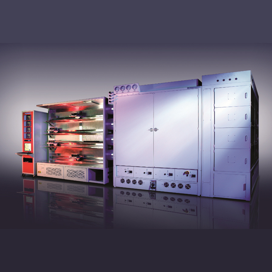
nSeries OC Sorters

4 station open carrier wafer sorter
50mm to 200mm wafer sizes.
Dual paddle buffering for same carrier sorting
350wph OCR / 800wph transfer
smallest 4 station single level footprint available in industry
4 station for better queuing and larger on tool splits
Many concurrent wafer size options available
All sorter+ options can be added on this tool size
Optional AUTOTEACH
Sorter+
inspection and metrology options for wafer sorters

hologenix slip finder
addition of slipfinder hardware and software
wafer slip is detected and measured using propriety Hologenix lighting and software
typical usage in wafer manufacturing, SOI and EPI
recipes can scan outer wafer edge, center of wafer, both or entire wafer

wafer thickness measurements
AVG thickness / TTV / bow / warp
single center point or radial profiling
confocal laser or white light interferometer depending on application
function can be added to any typical sorting recipe
typical recipes bin wafer based on thickness

option for any system using OCR
measures scribe location against a qualified location
automated characterization
automated inspection
function can be added to any typical sorting recipe
includes GEM/SECS reporting for X/Y and linear offests
limits monitoring and alarms

Top and Bottom Bevel Inspection Option
bolt on application for NADA or PST sorters
inspection option which scans the wafer bevel for cracks and chips
standard ascii and SECS/GEM reporting with defect size and location
optional image capture and industry standard XY Report Formating
captures defects down to 0.5mm
function can be added to any typical sort recipe
lastest generation seeing defects down to 60um

flip option for wafer flip applications
180 degree for standard wafer flip
90 degree quartz carrier vertical loading

hologenix dimple detection
addition of dimple hardware and software
dimples are detected and measured using propriety Hologenix lighting and software
typical usage in Si wafer manufacturing and MEMS markets
whole wafer image processing or magnified version are available
optional stocker and AGV integrated E84 delivery

front side bright light inspection
bolt on application for NADA or PST sorters
wafer topside ONLY visual inspection
joystick control or programmable recipe control with pass/fail button
function can be added to any typical sorting recipe
其他半导体检测仪Sorter的工作原理介绍
其他半导体检测仪Sorter的使用方法?
Sorter多少钱一台?
其他半导体检测仪Sorter可以检测什么?
其他半导体检测仪Sorter使用的注意事项?
Sorter的说明书有吗?
其他半导体检测仪Sorter的操作规程有吗?
其他半导体检测仪Sorter报价含票含运吗?
Sorter有现货吗?
企业名称
赛伦科技(北京)有限责任公司
企业信息已认证
企业类型
有限责任公司(外商合资)
信用代码
110000410283047
成立日期
2006-03-06
注册资本
美元8万元
经营范围
许可经营项目:无一般经营项目:电子技术、新能源技术的研发及技术咨询;销售自行研发的产品;批发电子设备、半导体设备、集成电路加工设备、集成电路检测设备及以上产品的零备件、科学仪器及仪表、家用电器,提供上述产品的技术服务.(未取得行政许可的项目除外)(知识产权出资0.8万美元。)理富,才清华
赛伦科技(上海)办事处
公司地址
上海市黄浦区陆家浜路1378号万事利大厦601室
客服电话
公司名称: 赛伦科技(上海)办事处
公司地址: 上海市黄浦区陆家浜路1378号万事利大厦601室 联系人: 吴13817915874 邮编: 200011 联系电话: 400-860-5168转2024
仪器信息网APP

展位手机站