
 关注
关注
已关注

![]() 已认证
已认证
粉丝量 0
400-860-5168转1446
仪器信息网认证电话,请放心拨打
核心参数
产地类别: 进口
定位检测噪声: <0.15nm RMS
样品尺寸: <15mm
样品台移动范围: 200x200微米


400-860-5168转1446
![]()
|

|

|
|
Additional Information | ||
MadPLL® Brochure | Laser Focus World Article  NANOPOSITIONING: Piezo­electric nano­positioners forge low-cost atomic force microscope | AFM Video Tutorial |
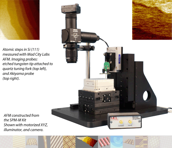
MadPLL® Sensor Probe Board Drawing  | Application Notes: SPM-004 "Building an AFM with motorized XYZ and camera" | |
Related Products |
|
MCL关注纳米扫描探针SPM-M Kit的工作原理介绍
扫描探针SPM-M Kit的使用方法?
MCL关注纳米SPM-M Kit多少钱一台?
扫描探针SPM-M Kit可以检测什么?
扫描探针SPM-M Kit使用的注意事项?
MCL关注纳米SPM-M Kit的说明书有吗?
MCL关注纳米扫描探针SPM-M Kit的操作规程有吗?
MCL关注纳米扫描探针SPM-M Kit报价含票含运吗?
MCL关注纳米SPM-M Kit有现货吗?
更多![]()
更多![]()
采用基于NADPH的荧光寿命成像法选择性探测多核形细胞中NADPH氧化酶
NADPH oxidase (NOX2) is a multisubunit membrane-bound enzyme complex that, upon assembly in activated cells, catalyses the reduction of free oxygen to its superoxide anion, which further leads to reactive oxygen species (ROS) that are toxic to invading pathogens, for example, the fungus Aspergillus fumigatus. Polymorphonuclear cells (PMNs) employ both nonoxidative and oxidative mechanisms to clear this fungus from the lung. The oxidative mechanisms mainly depend on the proper assembly and function of NOX2. We identified for the first time the NAD(P)H-dependent enzymes involved in such oxidative mechanisms by means of biexponentialNAD(P)H-fluorescence lifetime imaging (FLIM). A specific fluorescence lifetime of 3670±140 picoseconds as compared to 1870 picoseconds for NAD(P)H bound to mitochondrial enzymes could be associated with NADPH bound to oxidative enzymes in activated PMNs. Due to its predominance in PMNs and due to the use of selective activators and inhibitors, we strongly believe that this specific lifetime mainly originates from NOX2. Our experiments also revealed the high site specificity of the NOX2 assembly and, thus, of the ROS production as well as the dynamic nature of these phenomena. On the example of NADPH oxidase, we demonstrate the potential of NAD(P)H-based FLIM in selectively investigating enzymes during their cellular function.
其他
2011/03/27
北京欧兰科技发展有限公司
公司地址
北京市海淀区上地十街1号辉煌国际中心1号楼1006室
客服电话
公司名称: 北京欧兰科技发展有限公司
公司地址: 北京市海淀区上地十街1号辉煌国际中心1号楼1006室 联系人: 李俊杰 邮编: 100085 联系电话: 400-860-5168转1446
仪器信息网APP

展位手机站