为您推荐相似的其他
在科研中,很多用户需要用到光栅或点阵这些周期性的结构。有时用户不需要研究微纳米加工工艺,这样如果能花费低廉的价格买到这些成品将十分方便,只要接着从事后续的工作就可以了;有的用户自已拥有微纳米加工设备及经验,但纳米量级的尺寸要采用电子束曝光的方法来进行光刻,若有效面积超过1平方厘米,占机时间会很长,并需要调整电子束光刻及干法刻蚀工艺来优化成品。
鉴于此,我们向用户提供光栅及点阵的纳米结构成品。衬底材料为硅单晶,可广泛应用于各类科学研究。
产品类型:
标准模板一
○ 光栅纳米结构模板 (线条+间距)
○ 二维纳米模板(矩形或六边形)
标准模板二
○ 光栅结构
○ 柱状点阵模板
○ 孔阵模板
2x2cm2模板
四英寸模板
六英寸模板
标准模板一
我们可提供纳米级微结构,衬底材料为硅单晶,广泛应用于科学研究。批量生产,质量有保证,且性价比高。
产品精度:
线宽/深度:±15%
周期精度:优于0.5%
衬底宽度和高度误差:± 0.2 mm
衬底厚度:0.675 ± 0.050 mm
具体规格如下表所示:
光栅纳米结构模板 (线条+间距) Linear Nanostamps (line+space)
| 序号 | 周期 | 沟槽深度 | 占空比 ① | 线宽 ② | 样片尺寸③ |
1 | 139 nm | 50 nm | 50% | 69.5 nm | 12.5×12.5×0.7 mm |
2 | 139 nm | 50 nm | 50% | 69.5 nm | 25×25×0.7 mm ⑤ |
3 | 278 nm④ | 110 nm | 50% | 139 nm | 12.5×12.5×0.7 mm |
4 | 416.6 nm | 110 nm | 50% | 208 nm | 12.5×12.5×0.7 mm |
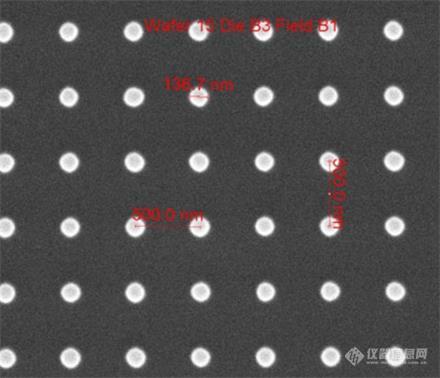
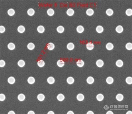
5 | 500 nm | multiple ⑥ | 44% | 220 nm | 8×8.3×0.7 mm |
6 | 500 nm | multiple ⑥ | 60% | 300 nm | 8×8.3×0.7 mm |
7 | 555.5 nm | 110 nm | 50% | 278 nm | 20×9×0.7 mm |
8 | 555.5 nm | 140 nm | 50% | 278 nm | 20×9×0.7 mm |
9 | 555.5 nm | 110 nm | 29% | 158 nm | 20×9×0.7 mm |
10 | 555.5 nm | 140 nm | 29% | 158 nm | 20×9×0.7 mm |
11 | 600 nm | multiple ⑥ | 43% | 260 nm | 8×8.3×0.7 mm |
12 | 600 nm | multiple ⑥ | 55% | 330 nm | 8×8.3×0.7 mm |
13 | 606 nm | 190 nm | 50% | 303 nm | 29×12×0.7 mm |
14 | 606 nm④ | 190 nm | 50% | 303 nm | 29×12×0.7 mm |
15 | 606 nm | 190 nm | 50% | 303 nm | 29×24.2×0.7 mm ⑤ |
16 | 675 nm | 170 nm | 32% | 218 nm | 24×10×0.7 mm |
17 | 675 nm | 170 nm | 32% | 218 nm | 24×30.4×0.7 mm ⑤ |
18 | 700 nm | multiple ⑥ | 47% | 330 nm | 8×8.3×0.7 mm |
19 | 700 nm | multiple ⑥ | 55% | 375 nm | 8×8.3×0.7 mm |
20 | 833.3 nm | 200 nm | 50% | 416 nm | 12.5×12.5×0.7 mm |
21 | 833.3 nm | 200 nm | 50% | 416 nm | 25×25×0.7 mm ⑤ |
①占空比表示线宽和周期的比率。
③第二个尺寸相当于沟槽的长度。
④scientific" grade offered at a discount. It has at least 80% of usable area. Up to 80/100 scratch/dig/particles and irregular substrate shape may present.
⑤可定做更大尺寸
⑥深度可做成150, 250 和 350 nm。
二维纳米模板(矩形或六边形)2D nanostamps (rectangular and hexagonal lattice)
序号 | 周期 | 晶格类型 | 沟槽深度 | 特征宽度 | 衬底尺寸 |
1 | 500 nm | rect post | multiple ① | 135 nm | 8×8.3×0.7 mm |
2 | 500 nm | rect post | multiple ① | 210 nm | 8×8.3×0.7mm |
3 | 600 nm | rect post | multiple ① | 195 nm | 8×8.3×0.7mm |
4 | 600 nm | rect post | multiple ① | 275 nm | 8×8.3×0.7mm |
5 | 700 nm | rect post | multiple ① | 260 nm | 8×8.3×0.7mm |
6 | 700 nm | rect post | multiple ① | 350 nm | 8×8.3×0.7mm |
7 | 500 nm | hex post | multiple ① | 165 nm | 8×8.3×0.7mm |
8 | 600 nm | hex post | multiple ① | 165 nm | 8×8.3×0.7mm |
9 | 600 nm | hex post | multiple ① | 240 nm | 8×8.3×0.7mm |
10 | 700 nm | hex post | multiple ① | 220 nm | 8×8.3×0.7mm |
11 | 700 nm | hex post | multiple ① | 290 nm | 8×8.3×0.7mm |
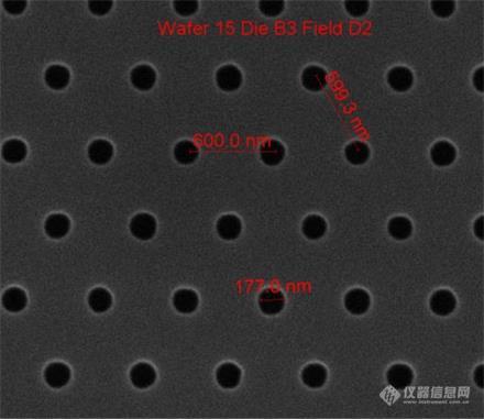
12 | 600 nm | hex hole | multiple ① | 180 nm | 8×8.3×0.7mm |
13 | 700 nm | hex hole | multiple ① | 200 nm | 8×8.3×0.7mm |
14 | 700 nm | hex hole | multiple ① | 290 nm | 8×8.3×0.7mm |
①深度可做成150, 250 和 350 nm
| rect post: | hex post: |
 |  |
| hex hole: | |
 |
标准模板二
我们可提供纳米级微结构,衬底材料为硅单晶,广泛应用于科学研究。批量生产,质量有保证,且性价比高。
产品精度:
| 产品说明:
|
具体规格如下表所示:
光栅结构(周期,线宽,高度,有效面积,衬底尺寸)
| Part No | Description | Image |
| Pattern 10 | Line grating Period: 70 nm Width: 25 nmor 35 nm Height: 32nmor 40 nm Area: 4x 0.5 x 1.2 mm2 Substrate: Si 20 x 20 mm2 | 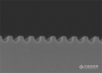 |
| Pattern 2 | Line grating Period: 300 nm Width: 170 nm Height: 210 nm Area: 30 x 30 mm2 Substrate: Si 30 x 30 mm2 | 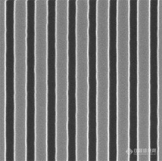 |
| Pattern 23 | Line arry Period: 150 nm Width: 75 nm Height: 116 nm Area:25 x25 mm2 Substrate:Si 30 x 30 mm2 | 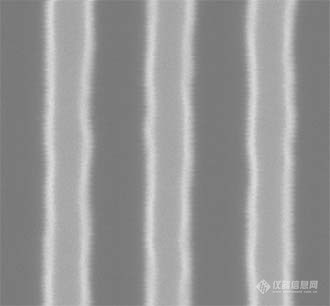 |
柱状点阵模板(周期,柱直径,高度,有效面积,衬底尺寸)
| Part No | Description | Image |
| Pattern 1 | Square pillar array Period: 300 nm Diameter: 145 nm Height: 170 nm Area: 14 x 14 mm2 Substrate: Si 14 x 14 mm2 | 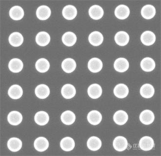 |
| Pattern 6 | High-resolution pillar array Period: 35 nmand 42 nm Diameter: 15 - 20 nm Height: 25nm Area: each period >25x25 um2 Substrate: Si 12.5 x 12.5 mm2 | 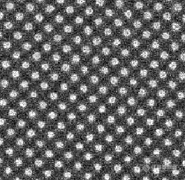 |
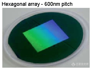
| Pattern 3 | Hexagonal pillar array Period: 600 nm Diameter: 300 nm Height: 310 nm Area: 20 x 20 mm2 Substrate: Si 20 x 20 mm2 |  |
| Pattern 15 | Hexagonal pillar array Period: 750 nm Diameter: 325 nm Height: 260 nm Area: 25 x 25 mm2 Substrate: Si 25 x 25 mm2 | 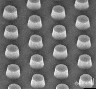 |
| Pattern 7 | Hexagonal pillar array Period: 1000 nm Diameter: 400 nm Height: 280 nm Area: 20 x 20 mm2 Substrate: Si 26 x 26 mm2 | 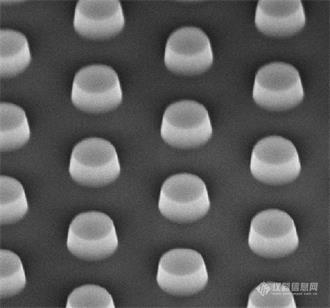 |
| Pattern 17 | Hexagonal pillar array Period: 1010 nm Diameter: 470 nm Height: 750 nm Area: 25 x 25 mm2 Substrate: Si (0.7mm) 25 x 25 mm2 | 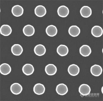 |
| Pattern 20 | Hexagonal pillar array Period: 3000 nm Diameter: 1800 nm Height: 1200 nm Area: 20 x 20 mm2 Substrate: Si 25 x 25 mm2 | 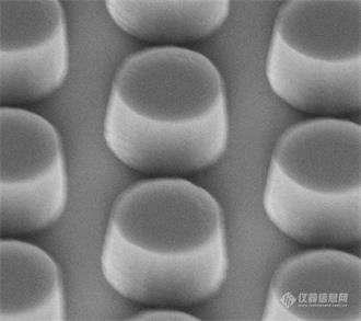 |
孔阵模板(周期,孔直径,高度,有效面积,衬底尺寸)
| Part No | Description | Image |
| Pattern 11 | Square hole array Period: 90 nm Diameter: 45 nm Height: 50 nm Area: 4x 0.6 x 0.6 mm2 Chip size: 15 x 15 mm2 | 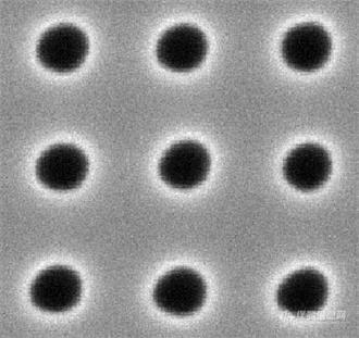 |
| Pattern 13 | Square hole array Period: 300 nm Diameter: 150 nm Height: 300 nm Area: 4 x 4 mm2 Chip size: 15 x 15 mm2 Substrate: Quartz (2.3 mm thick) | 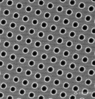 |
| Pattern 24 | Square hole array Period: 350 nm Diameter: 225 nm Height: 300 nm Area: 20 x 20 mm2 Substrate: Si 20 x 20 mm2 | 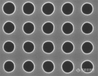 |
| Pattern 4 | Hexagonal hole array Period: 600 nm Diameter: 300 nm Height: 50 nm, 450 nm Area: 20 x 20 mm2 Substrate: Si 20 x 20 mm2 | 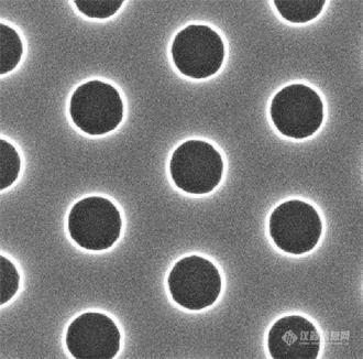 |
| Pattern 5 | Hexagonal hole array Period: 600 nm Diameter: 400 nm Height: 680 nm Area: 20 x 20 mm2 Substrate: Si 20 x 20 mm2 | 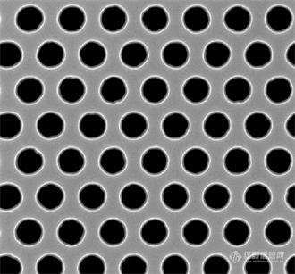 |
| Pattern 14 | Hole array on Rhombic lattice Period:* x=610nm, y=425nm Diameter: 150 nm Height: 300 nm Area: 20 x 20 mm2 Chip size: Si 24 x 24 mm2 * center-to-center distance in x and y | 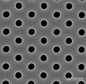 |
| Pattern 16 | Hexagonal hole array Period: 750 nm Diameter: 380 nm Height: 420 nm Area: 25 x 25 mm2 Substrate: Si 25 x 25 mm2 | 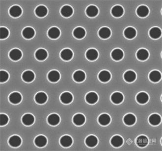 |
| Pattern 18 | Hexagonal hole array Period: 1010 nm Diameter: 490 nm Height: 470 nm Area: 25 x 25 mm2 Substrate: Si (1mm) 25 x 25 mm2 | 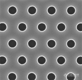 |
| Pattern 19 | Hexagonal hole array Period: 1500 nm Diameter: 780 nm Height: 550 nm Area: 25 x 25 mm2 Substrate: Si (1mm) 25 x 25 mm2 | 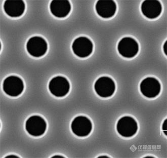 |
| Pattern 21 | Hexagonal hole array Period: 3000 nm Diameter: 1500 nm Height: 850 nm Area: 20 x 20 mm2 Substrate: Si 25 x 25 mm2 | 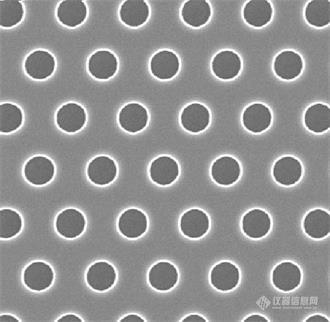 |
| Pattern 22 | Hexagonal hole array Period: 3000 nm Diameter: 1200 nm Height: 1500 nm Area: 20 x 20 mm2 Substrate: Si 25 x 25 mm2 | 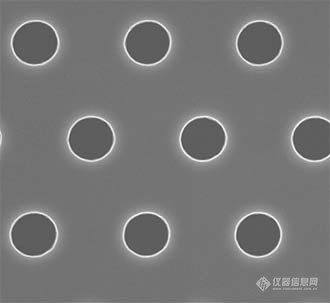 |
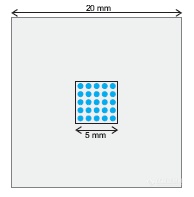
2x2cm2标准纳米压印模板
我们提供电子束光刻方法制备的硅模板,衬底尺寸为20x20mm2。图形分辨率高,有效区域为5x5mm2。批量生产,质量有保证,且性价比高。
产品精度:
|  |
具体规格如下表所示:
孔阵(矩形孔阵)
| 序号 | Product | Period | Area | Diameter / Height | 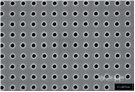 |
| 1 | P100s_h_5w5 | 100nm | 5x5mm2 | 50nm/ 100nm | |
| 2 | P150s_h_5w5 | 150nm | 5x5mm2 | 60nm/ 100nm | |
| 3 | P200s_h_5w5 | 200nm | 5x5mm2 | 70nm/ 100nm |
孔阵(六边形孔阵)
| 序号 | Product | Period | Area | Diameter / Height | 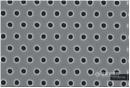 |
| 1 | P200h_h_5w5 | 200nm | 5x5mm2 | 80nm/ 100nm | |
| 2 | P300h_h_5w5 | 300nm | 5x5mm2 | 125nm/ 100nm | |
| 3 | P400h_h_5w5 | 400nm | 5x5mm2 | 150nm/ 100nm |
柱状点阵(矩形柱状点阵)
| 序号 | Product | Period | Area | Diameter / Height | 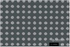 |
| 1 | P100s_p_5w5 | 100nm | 5x5mm2 | 50nm/ 100nm | |
| 2 | P150s_p_5w5 | 150nm | 5x5mm2 | 60nm/ 100nm | |
| 3 | P200s_p_5w5 | 200nm | 5x5mm2 | 80nm/ 100nm |
柱状点阵(六边形柱状点阵)
| 序号 | Product | Period | Area | Diameter / Height | 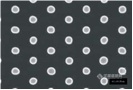 |
| 1 | P200h_p_5w5 | 200nm | 5x5mm2 | 70nm/ 100nm | |
| 2 | P300h_p_5w5 | 300nm | 5x5mm2 | 110nm/ 100nm | |
| 3 | P400h_p_5w5 | 400nm | 5x5mm2 | 120nm/ 100nm |
大面积四英寸模板
我们提供四英寸硅或石英模板,可用于压印工艺。批量生产制作,质量有保证且性价比高。
产品精度:
|  |
具体规格如下表所示:
Holes on Hexagonal Lattice(六边形孔阵)
| Part No | Product | Period | Diameter | Area | Max. Etch depth (Si/Quartz) | Image | ||
| 1 | P520h_h_20w20 | 520 nm | 260nm | 20x20 mm2 | 450 nm/200 nm | 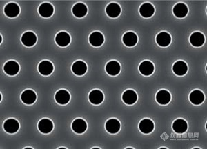 | ||
| 2 | P600h_h_46w46 | 600 nm | 300nm | 46x46 mm2 | 450 nm/200 nm | |||
| 3 | P600h_h_100d | 600 nm | 300nm | 4-inch | 450 nm/200 nm | |||
| 4 | P750h_h_51w51 | 750 nm | 350nm | 51x51 mm2 | 450 nm/200 nm | |||
| 5 | P780h_h_20w20 | 780 nm | 350nm | 20x20 mm2 | 450 nm/200 nm | |||
| 6 | P1000h_h_20w20 | 1000 nm | 400nm | 20x20 mm2 | 600 nm/300 nm | |||
| 7 | P1000h_h_51w51 | 1000 nm | 300nm~ 500nm | 51x51 mm2 | 600 nm/300 nm | |||
| 8 | P1500h_h_20w20 | 1500 nm | 400nm~ 650nm | 20x20 mm2 | 600 nm/300 nm | |||
| 9 | P1500h_h_51w51 | 1500 nm | 400nm~ 650nm | 51x51 mm2 | 600 nm/300 nm | |||
| 10 | P3000h_h_100d | 3000 nm | 600nm~ 1400nm | 4-inch | 1000 nm/400 nm | |||
Holes on Square Lattice(矩形孔阵)
| Part No | Product | Period | Diameter | Area | Max. Etch depth (Si/Quartz) | Image | ||
| 11 | P350s_h_20w20 | 350 nm | 250nm | 20x20 mm2 | 300 nm/150 nm | 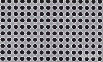 | ||
| 12 | P350s_h_100d | 350 nm | 250nm | 100dia | 300 nm/150 nm | |||
Pillars on Hexagonal Lattice(六边形柱状)
| Part No | Product | Period | Diameter | Area | Max. Etch depth (Si/Quartz) | Image | ||
| 13 | P600h_p_46w46 | 600 nm | 300nm | 46x46 mm2 | 450 nm/200 nm | 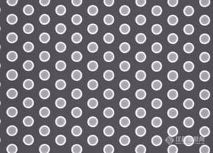 | ||
| 14 | P600h_p_100d | 600 nm | 300nm | 4-inch | 450 nm/200 nm | |||
| 15 | P750h_p_51w51 | 750 nm | 350nm | 51x51 mm2 | 450 nm/200 nm | |||
| 16 | P780h_p_20w20 | 780 nm | 350nm | 20x20 mm2 | 450 nm/200 nm | |||
| 17 | P1000h_p_20w20 | 1000 nm | 400nm | 20x20 mm2 | 600 nm/300 nm | |||
| 18 | P1000h_p_51w51 | 1000 nm | 300nm~ 500nm | 51x51 mm2 | 600 nm/300 nm | |||
| 19 | P1500h_p_20w20 | 1500 nm | 400nm~ 650nm | 20x20 mm2 | 600 nm/300 nm | |||
| 20 | P1500h_p_51w51 | 1500 nm | 400nm~ 650nm | 51x51 mm2 | 600 nm/300 nm | |||
| 21 | P3000h_p_100d | 3000 nm | 600nm~ 1400nm | 4-inch | 1000 nm/400 nm | |||
Pillars on Square Lattice(矩形柱状点阵)
| Part No | Product | Period | Diameter | Area | Max. Etch depth (Si/Quartz) | Image | ||
| 22 | P150s_p_30w30 | 150 nm | 75nm | 30x30 mm2 | 75 nm/ — | 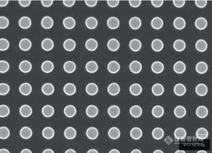 | ||
| 23 | P250s_p_30w30 | 250 nm | 110nm | 30x30 mm2 | 200 nm/100 nm | |||
| 24 | P300s_p_30w30 | 300 nm | 130nm | 30x30 mm2 | 200 nm/100 nm | |||
| 25 | P400s_p_30w31 | 400nm | 250nm | 30x30 mm3 | 200 nm/100 nm | |||
| 26 | P500s_p_30w30 | 500 nm | 250nm | 30x30 mm2 | 450 nm/200 nm | |||
Linear Gratings(光栅结构)
| Part No | Product | Period | Width | Area | Max. Etch depth (Si/Quartz) | Image | ||
| 27 | P150L_p_30w30 | 150nm | 70nm | 30x30 mm2 | 75 nm/ — | 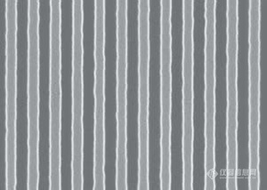 | ||
| 28 | P250L_p_30w30 | 250nm | 110nm | 30x30 mm2 | 200 nm/100 nm | |||
| 29 | P300L_p_30w30 | 300nm | 130nm | 30x30 mm2 | 200 nm/100 nm | |||
| 30 | P400L_p_30w30 | 400nm | 200nm | 30x30 mm2 | 200 nm/100 nm | |||
| 31 | P500L_p_30w30 | 500nm | 250nm | 30x30 mm2 | 450 nm/200 nm | |||
Multi-pattern(复合结构)
Part No | Product | Description | Diameter | Period | Area | Max. Etch depth (Si/Quartz) |
| 32 | MHSL_400-800 | Linear, hexagonal, square array combination, Periods: 400-800nm | pitch dependent | ho, les/ lines | each period,7.5mm x 7.5mm | 400 nm/150 nm |
| 33 | MP250L300 | Multi-period linear grating combination 1, Periods: 250nm, 275nm, 300nm | Linewidth(+/15nm): 90/250 100/275 120/300 | lines | each period,7mm x 7mm | 200 nm/100 nm |
| 34 | MP300L600 | Multi-period linear grating combination 2, Periods: 300nm, 400nm, 500nm, 600nm | Linewidth(+/15nm): 90/250 100/275 120/300 | lines | each period,10mm x 10mm | 300 nm/150 nm |
保修期: 1年
是否可延长保修期: 是
现场技术咨询: 无
免费培训: 无
免费仪器保养: 无
保内维修承诺: 无
报修承诺: 无
EULITHA其他半导体检测仪Template的工作原理介绍
其他半导体检测仪Template的使用方法?
EULITHATemplate多少钱一台?
其他半导体检测仪Template可以检测什么?
其他半导体检测仪Template使用的注意事项?
EULITHATemplate的说明书有吗?
EULITHA其他半导体检测仪Template的操作规程有吗?
EULITHA其他半导体检测仪Template报价含票含运吗?
EULITHATemplate有现货吗?