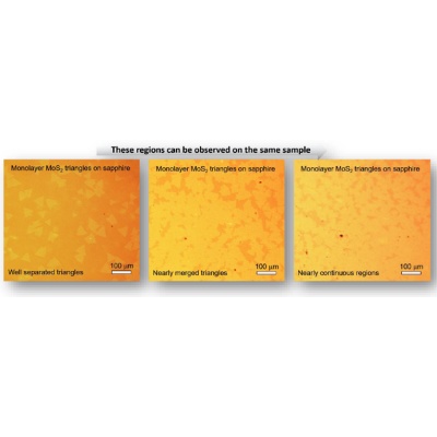
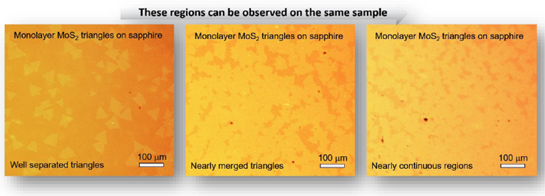
Isolated monolayer thickness MoS2 are grown onto c-cut (0001) sapphire substrates. This particular product contains monolayer thickness MoS2 triangular flakes randomly distributed across sapphire substrate. While some regions reach continuity with coalesced MoS2 triangles, this sample contains well-separated triangles for advanced spectroscopy, microscopy, and electronic measurements. Synthesized monolayer MoS2 triangles are highly luminescent and Raman spectroscopy studies also confirm the monolayer thickness.
Sample Properties.
Sample size | 1cm x 1cm square shaped |
Substrate type | (0001) c-cut sapphire |
Coverage | Isolated and Partially Merged Monolayer Triangles |
Electrical properties | 1.85 eV Direct Bandgap Semiconductor |
Crystal structure | Hexagonal Phase |
Unit cell parameters | a = b = 0.313 nm, c = 1.230 nm, α = β = 90°, γ = 120° |
Production method | Atmospheric Pressure Chemical Vapor Deposition (APCVD) |
Characterization methods | Raman, photoluminescence, TEM, EDS |
Specifications
1) Identification. Well-separated MoS2 domains across c-cut sapphire
2) Physical dimensions. One centimeter in size. Larger sizes up to 2-inch wafer-scale available upon requests.
3) Smoothness. Atomically smooth surface with roughness < 0.15 nm.
4) Uniformity. Highly uniform surface morphology. MoS2 triangles are scattered across sample
5) Purity. 99.9995% purity as determined by nano-SIMS measurements
6) Reliability. Repeatable Raman and photoluminescence response
7) Crystallinity. High crystalline quality, Raman response, and photoluminescence emission comparable to single crystalline monolayer flakes.
8) Substrate. c-cut Sapphire but our research and development team can transfer MoS2 triangles onto variety of substrates including PET, quartz, and SiO2/Si without significant compromising of material quality.
9) Defect profile. MoS2 monolayer triangles do not contain intentional dopants or defects. However, our technical staff can produce defected MoS2 using α-bombardment technique.
Supporting datasets [for Monolayer MoS2 Triangles on c-cut Sapphire]
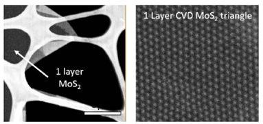
Transmission electron images (TEM) acquired from CVD grown MoS2 isolated triangles on c-cut sapphire confirming highly crystalline nature of monolayers
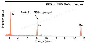
Energy dispersive X-ray spectroscopy (EDX) characterization on CVD grown MoS2 isolated triangles on c-cut sapphire confirming Mo:S 1:2 ratios
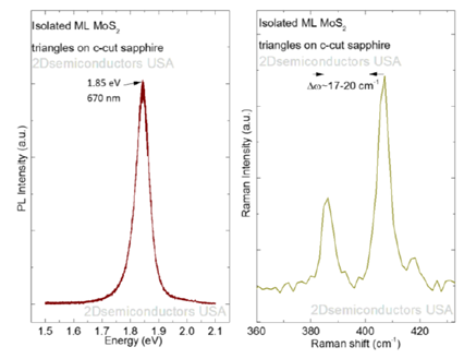
Room temperature photoluminescence spectroscopy (PL) and Raman spectroscopy (Raman) measurements performed on CVD grown MoS2 isolated triangles on c-cut sapphire. Raman spectroscopy measurement confirm monolayer nature of the CVD grown samples and PL spectrum display sharp and bright PL peak located at 1.85 eV in agreement with the literature.
基于蓝宝石衬底的三角形单层二硫化钼信息由上海巨纳科技有限公司为您提供,如您想了解更多关于基于蓝宝石衬底的三角形单层二硫化钼报价、型号、参数等信息,欢迎来电或留言咨询。
除供应基于蓝宝石衬底的三角形单层二硫化钼外,上海巨纳科技有限公司还可为您提供基于铜衬底的石墨烯、氨基化石墨烯、单层二硫化钼-纳米尺寸单层二硫化钼等产品,公司有专业的客户服务团队,是您值得信赖的合作伙伴。