
 关注
关注
已关注
![]() 已认证
已认证
粉丝量 0
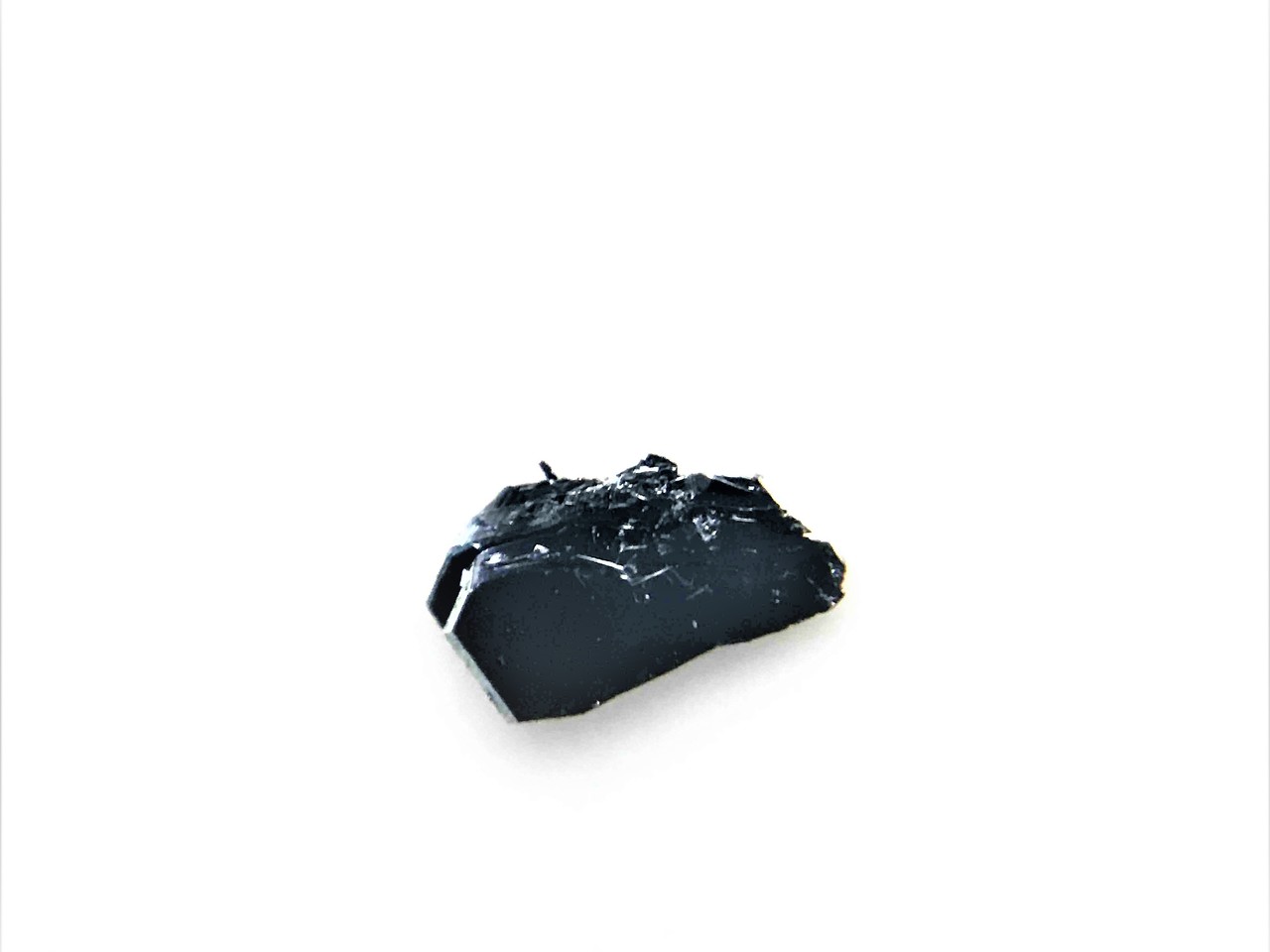
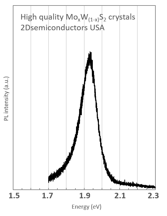
Our MoWS2 alloys with the chemical formula MoxW(1-x)S2 crystals perfectly crystallize in 2H phase and come at different alloy ratios x. Our crystals are grown using two different techniques through chemical vapor transport (CVT) or flux zone growth (see description of these two methods below) and their composition values were determined by XPS, SAED, and EDS measurements.. These crystals all possess extremely narrow PL bandwidths, display clean PL spectra, high carrier mobility, extremely clean and sharp XRD peaks, and negligible amount of defects (see published results as well as CVT vs. Flux based methods below). These crystals come with guaranteed alloying and valleytronic response, sharp PL, and good electronic response.
Important advantages of our crystals
1. Crystals come fully characterized using macro, micro, and nanoscale measurements (see below)
2. Thanks to our improved flux zone growth method, our crystals are homogeneously alloyed which means across the specimen you will only find one particular x composition.
3. No separation: Phase separation is commonly observed in 2D TMDCs alloys when cooling profiles are not controlled carefully. Our R&D team has worked over five (5) years to solely solve this problem.
Properties of layered MoWS2 alloys
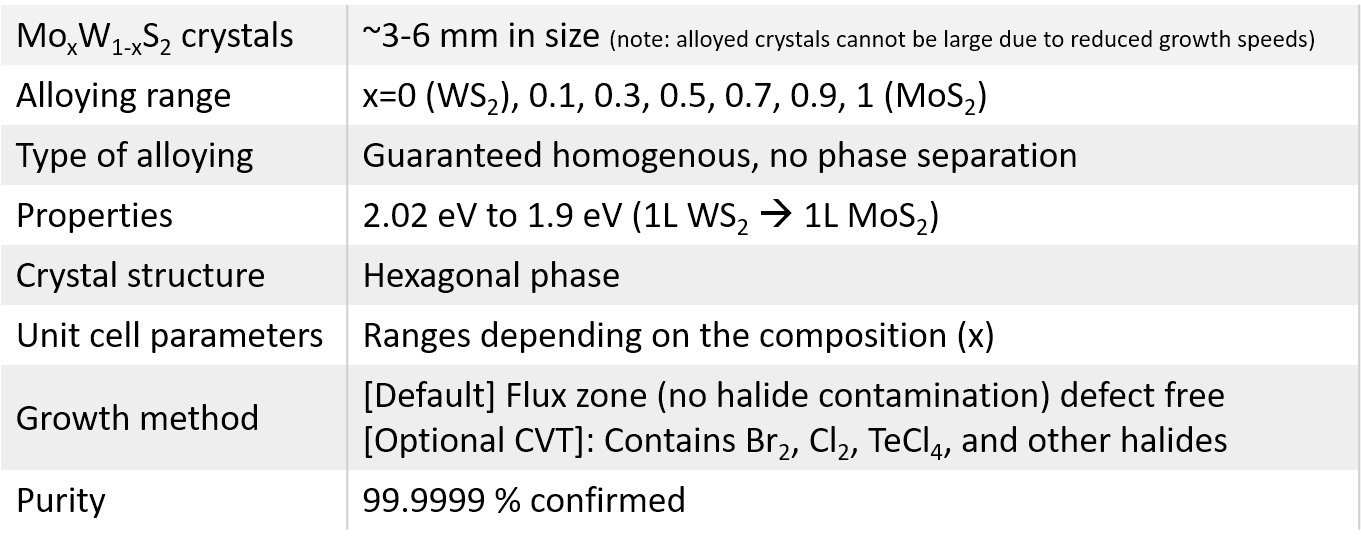
Growth method matters> Flux zone or CVT growth method? Contamination of halides and point defects in layered crystals are well known cause for their reduced electronic mobility, reduced anisotropic response, poor e-h recombination, low-PL emission, and lower optical absorption. Flux zone technique is a halide free technique used for synthesizing truly semiconductor grade vdW crystals. This method distinguishes itself from chemical vapor transport (CVT) technique in the following regard: CVT is a quick (~2 weeks) growth method but exhibits poor crystalline quality and the defect concentration reaches to 1E11 to 1E12 cm-2 range. In contrast, flux method takes long (~3 months) growth time, but ensures slow crystallization for perfect atomic structuring, and impurity free crystal growth with defect concentration as low as 1E9 - 1E10 cm-2. During check out just state which type of growth process is preferred. Unless otherwise stated, 2Dsemiconductors ships Flux zone crystals as a default choice.

企业名称
上海巨纳科技有限公司
企业信息已认证
企业类型
信用代码
310109000501433
成立日期
2009-04-01
注册资本
1000
经营范围
通信设备、光电源、生物科技专业领域内的技术开发、技术转让、技术咨询、技术服务;销售仪器仪表,电子元器件,机械设备及配件,通信设备及相关产品(除卫星地面接收装置),日用百货,从事货物及技术的进出口业务。【企业经营涉及行政许可的,凭许可证件经营】
上海巨纳科技有限公司
公司地址
上海市虹口区宝山路778号海伦国际大厦5楼
客服电话
公司名称: 上海巨纳科技有限公司
公司地址: 上海市虹口区宝山路778号海伦国际大厦5楼 联系人: 袁文军 邮编: 200081
仪器信息网APP

展位手机站