
 关注
关注
已关注

![]() 已认证
已认证
粉丝量 0
400-860-5168转0338
仪器信息网认证电话,请放心拨打
Growth of ZnO films by PED
2009-08-13 11:40
浏览:645次
分享:资料摘要:
下载本篇资料:
相关资料
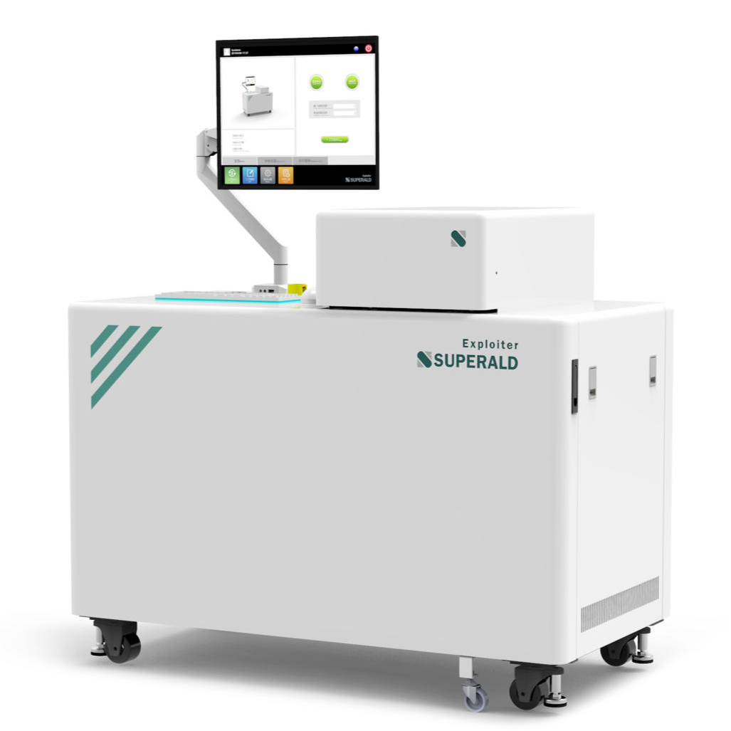
原速光电科技有限公司(Superald, LLC)是一家专注于原子层沉积(Atomic Layer Deposition,ALD)系统设计、工艺研发及技术咨询的高科技企业,为新能源、柔性显示、光学镀膜、生物医疗、催化、纳米技术等领域的薄膜研发和生产提供优质的技术服务和一体化解决方案,致力打造全球一流的薄膜材料制备平台。
脉冲激光沉积(Pulsed Laser Deposition)是一种用途广泛的薄膜沉积技术。脉冲激光快速蒸发靶材,生成与靶材组成相同的薄膜。PLD 的独特之处是能量源(脉冲激光)位于真空室的外面。这样,在材料合成时,工作压力的动态范围很宽,达到10-10 Torr ~ 100 Torr。通过控制镀膜压力和温度,可以合成一系列具有独特功能的纳米结构和纳米颗 粒。另外,PLD 是一种“ 数字” 技术,在纳米尺度上进行工艺控制(Å/pulse)。
万事创新(MIPS) 是⼀家全球性环境检测仪器公司,由新加坡国⽴⼤学化学与⼯程领域的专家团队建⽴。 开发新颖与精准的传感分析检测技术和产品以改善和保护环境。主要涉及灵敏分析检测仪器及其⾃动化和数据实时传输与监控。
1、将高温能力扩展到1000°C–超出NanoTest Vantage提供的850°C。 2、将低温能力提高至-40°C,且无样品结霜。 3、超低的热漂移归因于与NanoTestVantage相同的仪器设计原理。 4、完整的纳米力学测试(例如压痕、划痕、磨损、摩擦、冲击)。 5、 能够填充气体以匹配材料操作环境。
公司名称: 北京正通远恒科技有限公司
公司地址: 北京市朝阳区胜古中路2号院7号楼A座611室 联系人: 邮编: 100029 联系电话: 400-860-5168转0338
仪器信息网APP

展位手机站