当前位置: 仪器信息网 > 行业主题 > >

模特假人

仪器信息网模特假人专题为您整合模特假人相关的最新文章,在模特假人专题,您不仅可以免费浏览模特假人的资讯, 同时您还可以浏览模特假人的相关资料、解决方案,参与社区模特假人话题讨论。

模特假人相关的耗材

  • 二碲化钼晶体(99.995%) 1T-MoTe2(Molybdenum Ditelluride)
    二碲化钼晶体 1T-MoTe2(Molybdenum Ditelluride)晶体尺寸:~10毫米电学特性:金属晶体结构:单斜晶系晶胞参数:a = 0.621 nm, b = 0.347 nm, c = 1.383 nm, α = γ = 90°, β = 93.83 °晶体类型:合成晶体纯度:>99.995%X-ray diffraction on a 1T' -MoTe2 single crystal aligned along the (001) plane. XRD was performed at room temperature using a D8 Venture Bruker. The 5 XRD peaks correspond, from left to right, to (00l) with l = 2, 4, 6, 8, 10Powder X-ray diffraction (XRD) of a single crystal 1T' -MoTe2. X-ray diffraction was performed at room temperature using a D8 Venture Bruker.Stoichiometric analysis of a single crystal 1T' -MoTe2 by Energy-dispersive X-ray spectroscopy (EDX).Raman spectrum of a single crystal 1T' -MoTe2. Measurement was performed with a 785 nm Raman system at room temperature.
  • 二碲化钼晶体(99.995%) 2H-MoTe2(Molybdenum Ditelluride)
    二碲化钼晶体 2H-MoTe2(Molybdenum Ditelluride)晶体尺寸:~10毫米电学性能:N型半导体晶体结构:六边形晶胞参数:a = b = 0.353 nm, c = 1.396 nm, α = β = 90, γ = 120°晶体类型:合成晶体纯度:>99.995%X-ray diffraction on a MoTe2 single crystal aligned along the (001) plane. XRD was performed at room temperature using a D8 Venture Bruker. The 4 XRD peaks correspond, from left to right, to (00l) with l = 2, 4, 6, 8Powder X-ray diffraction (XRD) of a single crystal MoTe2. X-ray diffraction was performed at room temperature using a D8 Venture Bruker.Stoichiometric analysis of a single crystal 2H MoTe2 by Energy-dispersive X-ray spectroscopy (EDX).Raman spectrum of a single crystal 2H MoTe2. Measurement was performed with a 785nm Raman system at room temperature.
  • 二碲化钼(MoTe2)
    1、企业介绍泰州巨纳新能源有限公司:巨纳集团(Sunano Group)是能源行业的知名品牌。泰州巨纳新能源有限公司(Sunano Energy)是国内最早的从事石墨烯制备、性能检测及应用产品开发的公司之一,注册资本11000万元,有办公用房300多平方米,厂房和洁净室3000多平方米。核心研发团队主要由国内外知名高校博士组成,部分成员来自于2010年诺贝尔物理学奖小组,项目技术处于国际领先地位,在石墨烯领域拥有专利30余项。企业管理团队有丰富的成功创业经验,创新意识强,公司客户遍布全球。2、高质量二维晶体材料简介:二维晶体材料指的是以石墨烯为代表的单原子层及少数原子层厚度的晶体材料。巨纳集团除了提供石墨烯材料、设备、检测等一体化服务外,还联合荷兰HQ Graphene为全球客户提供高质量的类石墨烯二维晶体材料,并提供定制服务,以满足客户的不同需求。名称:二碲化钼(MoTe2) 纯度:>99.995% 尺寸:~6 mm-10 mm 属性:半导体
  • Metallic MoTe2 (1T' phase) 1T-二碲化钼晶体
    1T' metallic phase of MoTe2 crystals contain layers that are stacked together via van der Waals interactions and can be exfoliated into thin 2D layers. Our large size 1T' -MoTe2 vdW crystals are treated as gold standards in 2D materials field. They come with guaranteed environmental stability, negligible amount of point defects, highly metallic response, and high carrier mobility. Our MoTe2 crystals are synthesized two different methods (flux zone and chemical vapor transport). While flux zone provides extremely clean MoTe2 crystals, CVT method often introduces halide contaminants. For comparison between these tow methods, please see the information below.Characteristics of 1T' -MoTe2 crystals from 2Dsemiconductors USAGrowth method matters Flux zone or CVT growth method? Contamination of halides and point defects in layered crystals are well known cause for their reduced electronic mobility, reduced anisotropic response, poor e-h recombination, low-PL emission, and lower optical absorption. Flux zone technique is a halide free technique used for synthesizing truly semiconductor grade vdW crystals. This method distinguishes itself from chemical vapor transport (CVT) technique in the following regard: CVT is a quick (~2 weeks) growth method but exhibits poor crystalline quality and the defect concentration reaches to 1E11 to 1E12 cm-2 range. In contrast, flux method takes long (~3 months) growth time, but ensures slow crystallization for perfect atomic structuring, and impurity free crystal growth with defect concentration as low as 1E9 - 1E10 cm-2. During check out just state which type of growth process is preferred. Unless otherwise stated, 2Dsemiconductors ships Flux zone crystals as a default choice.
  • 2H-MoTe2 2H-二碲化钼晶体 (Molybdenum Ditelluride)
    2H semiconducting phase of MoTe2 crystals contain layers that are stacked together via van der Waals interactions and can be exfoliated into thin 2D layers. Our large size 2H-MoTe2 vdW crystals are treated as gold standards in 2D materials field. They come with guaranteed valleytronic performance, clean PL spectrum, perfect crystallization, and defect free structure. Our MoTe2 crystals are synthesized two different methods (flux zone and chemical vapor transport). While flux zone provides extremely clean MoTe2 crystals, CVT method often introduces halide contaminants. For comparison between these tow methods, please see the information below. If your research needs electronically doped MoTe2 crystals, please contact us.Characteristics of 2H-MoTe2 crystals from 2Dsemiconductors USAGrowth method matters Flux zone or CVT growth method? Contamination of halides and point defects in layered crystals are well known cause for their reduced electronic mobility, reduced anisotropic response, poor e-h recombination, low-PL emission, and lower optical absorption. Flux zone technique is a halide free technique used for synthesizing truly semiconductor grade vdW crystals. This method distinguishes itself from chemical vapor transport (CVT) technique in the following regard: CVT is a quick (~2 weeks) growth method but exhibits poor crystalline quality and the defect concentration reaches to 1E11 to 1E12 cm-2 range. In contrast, flux method takes long (~3 months) growth time, but ensures slow crystallization for perfect atomic structuring, and impurity free crystal growth with defect concentration as low as 1E9 - 1E10 cm-2. During check out just state which type of growth process is preferred. Unless otherwise stated, 2Dsemiconductors ships Flux zone crystals as a default choice.Partial List of Publications Using This ProductY. Li et. al. "Room-temperature continuous-wave lasing from monolayer molybdenum ditelluride integrated with a silicon nanobeam cavity"Nature Nanotechnology volume 12, pages 987–992 (2017)Control of Exciton Valley Coherence in Transition Metal Dichalcogenide Monolayers, Phys. Rev. Lett. 117, 187401 (2016)Tony Heinz Team "Optical Properties and Band Gap of Single- and Few-Layer MoTe2 Crystals" Nano Letters 2014, 14, 6231?6236Physical origin of Davydov splitting and resonant Raman spectroscopy of Davydov components in multilayer MoTe2 Q. J. Song, Q. H. Tan, X. Zhang, J. B. Wu, B. W. Sheng, Y. Wan, X. Q. Wang, L. Dai, and P. H. Tan Phys. Rev. B 93, 115409 (2016)Indirect-to-Direct Band Gap Crossover in Few-Layer MoTe2 Ignacio Gutiérrez Lezama et. al. Nano Letters 2015, 15 (4), pp 2336–2342 DOI: 10.1021/nl5045007Measurement of the optical dielectric function of monolayer transition-metal dichalcogenides: MoS2, MoSe2, WS2, and WSe2, Yilei Li, Alexey Chernikov, Xian Zhang, Albert Rigosi, Heather M. Hill, Arend M. van der Zande, Daniel A. Chenet, En-Min Shih, James Hone, and Tony F. Heinz Phys. Rev. B 90, 205422 (2014)M. Yankowitz et. al. "Intrinsic Disorder in Graphene on Transition Metal Dichalcogenide Heterostructures" Nano Letters, 2015, 15 (3), pp 1925–1929H. C. Diaz et.al. "Molecular beam epitaxy of the van der Waals heterostructure MoTe2 on MoS2: phase, thermal, and chemical stability" 2D Materials, Volume 2, Number 4 (2015)S. Vishwanath et. al. "MBE growth of few-layer 2H-MoTe2 on 3D substrates" Journal of Crystal Growth, 482, Pages 61-69 (2018)
  • 二碲化钼
    分类:半导体中文名称:二碲化钼英文名称:MoTe?纯度:≥99.9999%尺寸:~6 mm-10 mm
  • 大模场面积无截止波长单模光纤, 耐高温单模微结构光纤 35um
    这种单模微结构光纤通过结构上的优化,实现了导光窗口上的无截止单模传输特性。光纤的无截止单模特性使光纤在大模场面积实现单模传输,保证基模模场的光束质量,且与光纤纤芯尺寸无关。该光纤可应用于大模场面积的高功率激光传能,并极大降低了非线性效应的发生。技术参数特点无截止单模:导光窗口内所有波长单模传输,低数值孔径,与激光器耦合时,无需模式匹配,保持基模传输;提供定制设计生产:可以定制模场面积(MFD)大小、光纤零色散点可设计;结合保偏光纤:通过结构设计调整,提高光纤双折射,形成无截止波长单模传输保偏光纤;激光传能:纯石英材质无杂质,高激光损伤阈值、低光斑暗化;应用:模式滤波; 短脉冲传输;传能光纤、光缆;单模激光大功率传输; 多波长传输,波分复用;高精度激光熔接(单模高斯光斑)性能参数:MOF_SC_ESM20/153/173PIMOF_SC_ESM35/255/275PI纤芯直径:20 μm35 μm包层直径:153±3 μm255±3 μm 衰减系数:@1064 nm 20 dB/km@1064 nm 20 dB/km@1550 nm 15 dB/km@1550 nm 10 dB/km模场面积(*):225±30 μm2730±50 μm2芯包层材料:高纯熔融石英玻璃涂敷层直径:173±5 μm275±5 μm包层不圆度:≤0.1≤0.1涂层材料:聚酰亚胺/丙烯酸树脂长期使用温度:-55~300 ℃(聚酰亚胺)短期耐受温度:400 ℃(聚酰亚胺)筛选强度:100 kpsi*可定制更大模场面积光纤,定制模场面积范围:15~1200 μm2
  • Black Phosphorus粉末 黑磷粉末(1g)
    Black Phosphorus粉末 黑磷粉末(1g)纯度:99.9995%重量:1g制备方法:使用再提纯后的超高纯单质高真空密封烧结用途:用于生长制备二维晶体材料低维材料在线提供众多超高纯粉末,主要有:超高纯SnS2,超高纯SnSe2,超高纯SnTe2,超高纯ReS2,超高纯ReSe2,超高纯PtSe2,超高纯In2Se3,超高纯InSe,超高纯MoS2,超高纯MoSe2,超高纯MoTe2,超高纯WS2,超高纯WSe2,超高纯WTe2,超高纯Bi2S3,超高纯Bi2Se3,超高纯Bi2Te3,超高纯TiS2,超高纯TiSe2,超高纯TiTe2,超高纯GaS,超高纯GaSe,超高纯GaTe,超高纯GeS,超高纯GeSe,超高纯VSe2,超高纯NbS2,超高纯NbSe2,超高纯NbTe2,超高纯TaS2,超高纯TaSe2,超高纯TaTe2,超高纯ZrS3,超高纯ZrSe2,超高纯ZrSe3,超高纯TaTe3,超高纯NbReS2,超高纯NbReSe2,超高纯MoWS2,超高纯MoWSe2,超高纯WSSe等
  • 白色移液器Thermo Scientific Finnpipette digital
    前所未有的舒适体验 Finnpipette Digital移液器是目前最轻的移液器之一。弧形握柄和放松指靠大大提高了舒适感。人机工效学设计使您操作自然、减轻劳损。Finnpipette Digital移液器可整支高压灭菌。 微量移液 0.2-1000&mu l Finnpipette Digital移液器提供稳定可靠的移液操作,有双活塞的设计,能产生更强的排液能力,并防止毛细作用的发生,保证液体的完全转移。超强吹出可保证微量体积(0.2-50&mu l)的移液精准性。 大体积移液 1ml-10ml 凭借专业和36年的制造经验,Finnpipette 设计特有的大体积移液器。重量轻,使用方便,轻触推杆设计,可整支高压灭菌,更方便,更快捷,更准确。 独特的安全标签,也可换成您或家人的肖像,体现人性化设计。 有任何问题请联系:021-68654588-2166王小姐
  • Thermo Scientific Finnpipette digital白色移液器
    前所未有的舒适体验 Finnpipette Digital移液器是目前最轻的移液器之一。弧形握柄和放松指靠大大提高了舒适感。人机工效学设计使您操作自然、减轻劳损。Finnpipette Digital移液器可整支高压灭菌。 微量移液 0.2-1000&mu l Finnpipette Digital移液器提供稳定可靠的移液操作,有双活塞的设计,能产生更强的排液能力,并防止毛细作用的发生,保证液体的完全转移。超强吹出可保证微量体积(0.2-50&mu l)的移液精准性。 大体积移液 1ml-10ml 凭借专业和36年的制造经验,Finnpipette 设计特有的大体积移液器。重量轻,使用方便,轻触推杆设计,可整支高压灭菌,更方便,更快捷,更准确。 独特的安全标签,也可换成您或家人的肖像,体现人性化设计。 有任何问题请联系:021-68654588-2166王小姐
  • 二碲化钼
    简介:二维晶体材料指的是以石墨烯为代表的单原子层及少数原子层厚度的晶体材料,巨纳集团除了提供石墨烯材料、设备、检测等一体化服务外,还联合美国2D Semiconductors为全球客户提供高质量的二维晶体材料、粉体、溶液、薄膜等材料,并提供定制服务,以满足客户的不同需求。二碲化钼MoTe?
  • 平底烧瓶/短颈烧瓶
    平底烧瓶/短颈烧瓶由上海书培实验是设备有限公司为您专业生产提供,产品规格齐全,质量优越,欢迎客户来电咨询。产品使用时注意事项:平底烧瓶由于底部较平,当家人时受热会不均匀,英雌一般不做家人的反应器加热时,平底烧瓶要垫上石棉网,且不超过烧瓶体积的1/2,防止太多水在沸腾时容易溅出或是瓶内压力太大而爆炸产品相关规格介绍表格:产品名称规格单位单价平底烧瓶150ml/24支询价平底烧瓶250ml/19支询价平底烧瓶250ml/24支询价平底烧瓶500ml/19支询价平底烧瓶500ml/24支询价平底烧瓶1000ml/24支询价
  • 光子晶体光纤_微结构光纤(PCF)
    光子晶体光纤/微结构光纤(PCF)所属类别: ? 光纤/光纤器件 ? 其他特种光纤/光子晶体光纤 所属品牌: 产品简介 昊量光电提供各种定制型光子晶体光纤(PCF,微结构光纤)!光子晶体光纤(Photonic Crystal Fibers,PCF)又称为微结构光纤(Micro-Structured Fibers, MSF),这种光线的横截面上有较复杂的折射率分布,通常含有不同排列形式的小孔,这些小孔的尺度与光波波长大致在同一量级且贯穿器件的整个长度,光波可以被限制在低折射率的光纤芯区传播。昊量光电提供各种光子晶体光纤。 关键词:光子晶体光纤,Photonic Crystal Fibers, PCF,微结构光纤,Micro-Structured Fibers, 结构光纤 光子晶体光纤(Photonic Crystal Fibers,PCF)又称为微结构光纤(Micro-Structured Fibers, MSF),这种光线的横截面上有较复杂的折射率分布,通常含有不同排列形式的小孔,这些小孔的尺度与光波波长大致在同一量级且贯穿器件的整个长度,光波可以被限制在低折射率的光纤芯区传播。光子晶体光纤(微结构光纤)按照其导光机理可以分为两大类:折射率导光型(IG-PCF)和带隙引导型(PCF)。折射率引导型光子晶体光纤(微结构光纤,PCF)具有无截止单模特性 、大模场尺寸 /小模场尺寸和 色散可调特性等特性。广泛应用于色散控制 (色散平坦,零色散位移可以到800nm),非线性光学 (高非线性,超连续谱产生),多芯光纤 ,有源光纤器件(双包层PCF有效束缚泵浦光)和光纤传感等领域。空隙带隙型光子晶体光纤(微结构光纤,PCF) 具有易耦合,无菲涅尔反射,低弯曲损耗、低非线性和特殊波导色散等特点被广泛应用于高功率导光,光纤传感和气体光纤等方面。光子晶体光纤的发展为光纤传感 开拓了广阔的空间,尤其是在生物传感和气体传感方面为光纤传感技术带来新的发展。昊量光电提供各种光子晶体光纤及光子晶体光纤的定制化服务,昊量可以提供的产品及服务:材料:石英或硫化物提供各种定制服务可提供各种套管,接头及相应光线器件各种解决方案设计及模拟主要产品:1,基于石英的各种有源及无源光纤:保偏型光子晶体光纤,定制色散型光子晶体光纤,光子晶体光纤预制棒空气包层、双包层光子晶体光纤,LMA空心光纤,光子带隙光纤掺杂光子晶体光纤多心光子晶体光纤2,基于硫化物的光子晶体光纤超高非线性光纤(50,000/W*km)中红外光子晶体光纤定制化服务3,各种解决方案基础研究传感激光器光谱学主要应用:高功率低损耗近红外激光传输脉冲整形脉冲压缩非线性光学光纤传感超连续激光产生可调谐光纤耦合器多波长激光器光纤耦合 指标参数: 常规产品: 相关产品 覆盖紫外波段超连续激光器(320~1750nm) FROG 超短脉冲测量仪 啁啾布拉格光栅
  • A-Z系列晶体列表
    A-Z系列晶体列表A-F系列G-H系列L-N系列P-Z系列Al2O3GaTeLaAlO3PbWO4AlGaNLiTaO3PbF2AuGa2O3-?LiNbO3PbSAgGa:ZnOLiFPIN-PMN-PTAlN 单晶GdScO3LSATPMN-PTBaF2GaSbLaF3SrTiO3(国产,进口,Ti面终止SrTiO3)BaTiO3GaAsLiAlO2SrLaAlO4BGOGraphite(普通;热解)LGS 硅酸镓镧SrLaGaO4BSOGaSeLiGaO2Si(超薄Si片)Bi2Te3GGG(Gd3Ga5O12)LGT钽酸镓镧SiC(4H,6H,3C)Bi2Se3GeMgAl2O4SBNBi2Se2TeHg(1-x)Cd(x)TeMgF2SiO2(玻璃和单晶)Bi2Te2SeInPMgOSi-GeBP 黑磷InAsMoSe2TiO2(锐钛矿型,金红石型)CdSInSbMoS2TbScO3CsI (TI)KH2PO4MoTe2TGGCaCO3KTaO3MgO:LiNbO3TeO2Cu(单晶)KTa 1-X NbXO3NdCaAlO4WTe2CdSeKClNaClWS2Ce:Lu2SiO5KTNNb:SrTiO3(国产,进口)WSe2CdWO4HOPGNdGaO3YAGCdZnTeNaClYSZCdTeNiYAlO3CeF2YVO4CaF2ZnTeDyScO3ZnSeFe:SrTiO3ZnOFe3O4ZnSFe2O3Zero diffraction plate (Si和SiO2)
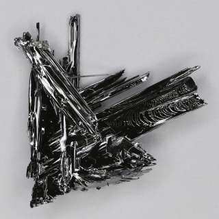
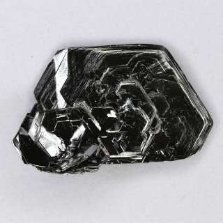
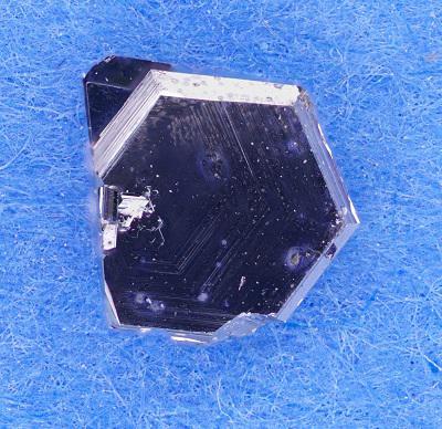
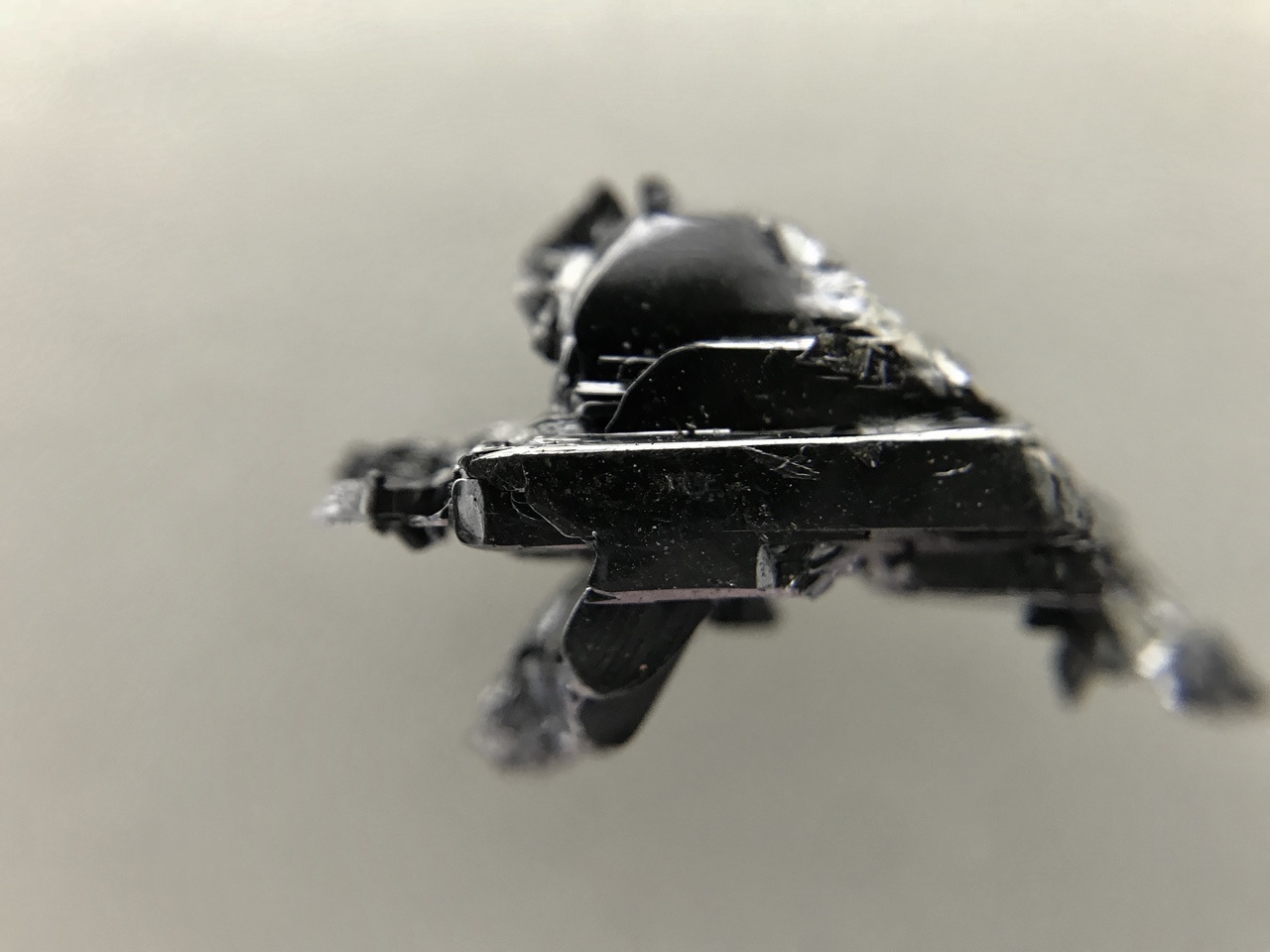
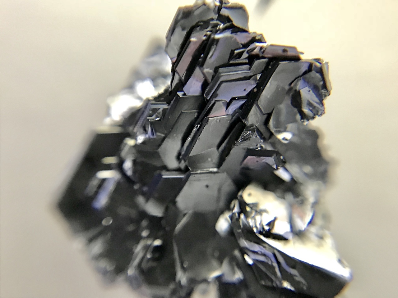
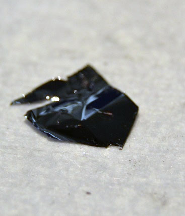
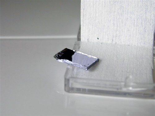
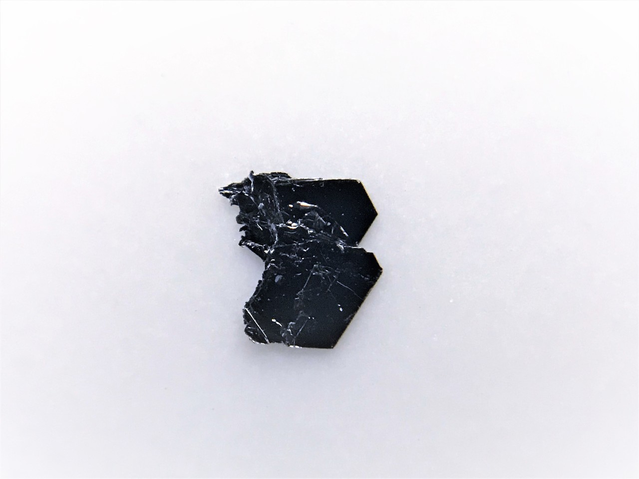
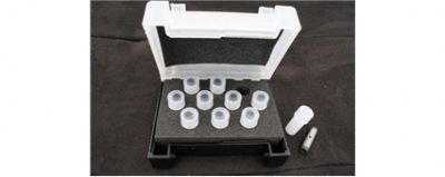
  • MoS2 二硫化钼晶体(合成)(Synthetic Molybdenum Disulfide)
    Single crystal highly oriented synthetic 2H-phase MoS2 crystals have been developed at our facilities in the USA starting from the powder making to crystallization. Our crystals are well-known for its low defect density, ultra-flat surfaces, and high crystallinity. Synthetic MoS2 samples have excellent layer by layer stacking with very small (0.3 degree) mosaic spread which enables you to exfoliate large monolayers with minimal amount of effort. Synthetic MoS2 is an indirect gap semiconductor (1.2 eV) but becomes highly luminescent in the monolayer from at 1.9 eV (quasi-particle / optical band gap). Synthetic MoS2 crystals are superior to natural MoS2 in in defects, electronic and optical performance, purity, and surface smoothness. Please also see our nature small, medium, and large MoS2 crystals.The properties of synthetic MoS2 crystalsPublications from this productSummary: Publications from Cornell, Washington, MIT, Berkeley, Stanford, and Princeton teams at top journals like Nature, Nature Materials, Nature Communications, Nano Letters, and Advanced MaterialsL. Zhang. et.al. "Photonic-crystal exciton-polaritons in monolayer semiconductors" Nature Communications volume 9, Article number: 713 (2018)Weigao Xu et al., "Correlated fluorescence blinking in two-dimensional semiconductor heterostructures", Nature 541, 62-67 (2017), link to article:http://www.nature.com/nature/journal/v541/n7635/full/nature20601.htmlManish Chhowalla team "Phase-engineered low-resistance contacts for ultrathin MoS2 transistors" Nature Materials DOI: 10.1038/NMAT4080X. Chen "Probing the electron states and metal-insulator transition mechanisms in molybdenum disulphide vertical heterostructures" Nature Communications 6, Article number: 6088 (2015) doi:10.1038/ncomms7088Measurement of the optical dielectric function of monolayer transition-metal dichalcogenides: MoS2, MoSe2, WS2, and WSe2, Yilei Li, Alexey Chernikov, Xian Zhang, Albert Rigosi, Heather M. Hill, Arend M. van der Zande, Daniel A. Chenet, En-Min Shih, James Hone, and Tony F. Heinz Phys. Rev. B 90, 205422 (2014)H. Wang et.al. "Ultrafast response of monolayer molybdenum disulfide photodetector" Nature Communications 6, Article number: 8831 (2015)Y. Jin "A Van Der Waals Homojunction: Ideal p–n Diode Behavior in MoSe2" Advanced Materials 27, 5534–5540 (2015)Tongay et. al. "Defects activated photoluminescence in two-dimensional semiconductors: interplay between bound, charged, and free excitons" Scientific Reports 3, Article number: 2657 (2013)X Li et al. "Determining layer number of twodimensional flakes of transition-metal dichalcogenides by the Raman intensity from substrates" Nanotechnology 27 (2016) 145704Tongay et.al. Thermally Driven Crossover from Indirect toward Direct Bandgap in 2D Semiconductors: MoSe2 versus MoS2 Nano Letters, 2012, 12 (11), pp 5576–5580Manish Chhowalla, "Two-dimensional semiconductors for transistors" Nature Reviews Materials 1, Article number: 16052 (2016) doi:10.1038/natrevmats.2016.52D. Wolverson et.al. "Raman Spectra of Monolayer, Few-Layer, and Bulk ReSe2: An Anisotropic Layered Semiconductor" ACS Nano, 2014, 8 (11), pp 11154–11164M. Yankowitz et. al. "Intrinsic Disorder in Graphene on Transition Metal Dichalcogenide Heterostructures" Nano Letters, 2015, 15 (3), pp 1925–1929H. C. Diaz et.al. "Molecular beam epitaxy of the van der Waals heterostructure MoTe2 on MoS2: phase, thermal, and chemical stability" 2D Materials, Volume 2, Number 4 (2015)A. Gul et.al. "Theoretical and experimental investigation of conjugation of 1,6-hexanedithiol on MoS2" Materials Research Express, 5 (3), 036415 (2018)C. Robert "Optical spectroscopy of excited exciton states in MoS2 monolayers in van der Waals heterostructures" Phys. Rev. Materials, 2, 011001 (R)
  • Restek Thermolite 隔垫 | 27142
    产品特点:Restek Thermolite 隔垫Restek Thermolite Septa● 可用于340°C的入口温度。*● 精密成型确保一致,精确的贴合。● 优秀的 puncturability。● 预处理并随时可用。● 采用超洁净泡罩包装。**● 一个Restek独家!注意:由于入口设计不同,给定入口设定点的实际隔垫温度可能因制造商而异。 Restek建议在Thermo TRACE和 Focus GC中仅使用BTO隔垫。*对于17mm 进样口,Thermolite 隔垫的最高温度为290°C。** 12.7mm 和17mm 隔垫包装在预先清洁的玻璃罐中。订货信息:Restek Thermolite SeptaCatalog #DiameterUnits2714211 mm (7/16")50-pk.2714311 mm (7/16")100-pk.27154Shimadzu Plug50-pk.27155Shimadzu Plug100-pk.
  • 沃特曼 采样膜 其他耗材
    WTP型聚四氟乙烯滤膜Whatman PTFE膜的化学稳定性和惰性使其适于腐蚀性强的有机溶剂、强酸和强碱。PTFE膜还非常适合于HPLC样品的制备。其天然的疏水性也非常适合于空气和气体灭菌。PTFE膜被压层到无纺布聚丙烯支撑网上用来提高强度和可操作性,并且可以在高达120°C高温下使用。订购信息-圆片WTP型聚四氟乙烯滤膜直径(mm)孔径(μm)描述货号包装/pack250.27582-0021002517590-002100470.27582-004100470.57585-0041004717590-004100TE型聚四氟乙烯滤膜Whatman PTFE膜的化学稳定性和惰性使其适于腐蚀性强的有机溶剂、强酸和强碱。PTFE膜还非常适合于HPLC样品的制备。其天然的疏水性也非常适合于空气和气体灭菌。PTFE膜被压层到无纺布聚丙烯支撑网上用来提高强度和可操作性,并且可以在高达120°C高温下使用。订购信息-圆片TE型聚四氟乙烯滤膜-TE35直径(mm)孔径(μm)描述货号包装/pack250.21041140550470.21041141150500.21041141350订购信息-圆片TE型聚四氟乙烯滤膜-TE36直径(mm)孔径(μm)描述货号包装/pack250.451041130550470.451041131150500.451041131350订购信息-圆片TE型聚四氟乙烯滤膜-TE37直径(mm)孔径(μm)描述货号包装/pack251104112055047110411211505011041121350订购信息-圆片TE型聚四氟乙烯滤膜-TE38直径(mm)孔径(μm)描述货号包装/pack375104111085047510411111505051041111350905104111162515051041113025
  • MoWTe2 二硒化钨钼晶体 (Molybdenum tungsten ditelluride)
    The first MoWTe2 ternary alloy. Large single crystal defect free molybdenum tungsten ditelluride (MoxW(1-x)Te2) crystals have been developed in our facilities and they have x=0.3,0.5, and 0.7 stoichiometric ratios. As they are semiconductor grade (99.9995% purity and perfect stoichiometry), you do not need to worry about amorphous phase, defects, or contamination. As the crystal size is large, they are ideal for exfoliating large monolayers. Single crystal MoWTe2 are very easy to exfoliate and the monolayer yield is high. Our crystals are grown using two different techniques through chemical vapor transport (CVT) or flux zone growth (see description of these two methods below) and their composition values were determined by XPS, SAED, and EDS measurements.. These crystals all possess extremely narrow PL bandwidths, display clean PL spectra, high carrier mobility, extremely clean and sharp XRD peaks, and negligible amount of defects (see published results as well as CVT vs. Flux based methods below ). These crystals come with guaranteed alloying and valleytronic response, sharp PL, and good electronic response.Important advantages of our crystals1. Crystals come fully characterized using macro, micro, and nanoscale measurements (see below)2. Thanks to our improved flux zone growth method, our crystals are homogeneously alloyed which means across the specimen you will only find one particular x composition.3. No separation: Phase separation is commonly observed in 2D TMDCs alloys when cooling profiles are not controlled carefully. Our R&D team has worked over five (5) years to solely solve this problem.During order please specify the desired composition ratio.Growth method matters Flux zone or CVT growth method? Contamination of halides and point defects in layered crystals are well known cause for their reduced electronic mobility, reduced anisotropic response, poor e-h recombination, low-PL emission, and lower optical absorption. Flux zone technique is a halide free technique used for synthesizing truly semiconductor grade vdW crystals. This method distinguishes itself from chemical vapor transport (CVT) technique in the following regard: CVT is a quick (~2 weeks) growth method but exhibits poor crystalline quality and the defect concentration reaches to 1E11 to 1E12 cm-2 range. In contrast, flux method takes long (~3 months) growth time, but ensures slow crystallization for perfect atomic structuring, and impurity free crystal growth with defect concentration as low as 1E9 - 1E10 cm-2. During check out just state which type of growth process is preferred. Unless otherwise stated, 2Dsemiconductors ships Flux zone crystals as a default choice.
  • 梅特勒 模块化变送器 M700
    M700 是液体分析领域在线测量的灵活选择。 M700X 应用于 ATEX Group II 、设备类别 2(1) 和气体/粉尘造成爆炸风险的场合。模块设计使 M700 胜任于各种测量任务。模块化设计意味着 M700 变送器允许模拟传感器和数字 ISM 传感器的混合测量,允许日后的扩展或修改。
  • 美国PE珀金埃尔默B0137113无涂层石墨管厂家特惠
    主要经营代理产品:美国PE(PerkinElmer)原子吸收光谱耗材、液相色谱耗材;美国安捷伦(Agilent)液相色谱耗材;美国沃特世(Waters)液相色谱耗材;德国耶拿(Analytik Jena):原子吸收光谱耗材;日本岛津(SHIMADZU):液相色谱耗材;美国戴安(DIONEX)离子色谱耗材;美国热电(ThermoFisher)原子吸收光谱耗材;美国瓦里安(Varian)光谱耗材;德国默克(MERCK)试剂、标液系列;美国Nalgene离心管、容器耗材等;韩国大韩磁力搅拌、电动搅拌器、电热套、加热板、高温炉系列;德国肖特实验室玻璃器皿系列;加拿大博朗全自动固相萃取仪等。PerkinElmer(PE)原子光谱常用石墨管、石墨锥、平台片规格型号如下:美国PE(Perkin Elmer)**石墨炉耗材配件(石墨炉型号:HGA300/400/500/600/700/800/850/900)B3000641--------THGA Tubes,partridged (5)横向加热石墨管5支/盒B0504033--------THGA Tubes,partridged (20) 横向加热石墨管20支/盒N3110147------- THGA Tubes,partridged (100) 横向加热石墨管100支/盒B3000653-------THGA Tubes with endcaps (5) 横向加热石墨管带端盖 5支/盒B3000655--------THGA Tubes with endcaps (20) 横向加热石墨管带端盖 20支/盒B3140361--------Ultra-clean THGA Graphite Tubes with Integrated Platform(5)超净石墨管5支/盒B3140362--------Ultra-clean THGA Graphite Tubes with Integrated Platform(20)超净石墨管20支/盒B0504035--------THGA Graphite contactcylinder 1pair(1) 横向加热石墨锥 1对/盒B0504036--------THGA Graphite contactcylinder 5pair (5) 横向加热石墨锥5对/盒B3002103--------Modified THGAcontactcylinder1pair (1) 改良的横向加热石墨锥1对/盒B3002102--------ModifiedTHGAcontactcylinder5pair(5) 改良的横向加热石墨锥 5对/盒B3001262--------HGA Graphite Tubes with integrated platforms (5) 集成弧型平台涂层石墨管5支/盒B3001264--------HGA Graphite Tubes with integrated platforms (20) 集成弧型平台涂层石墨管20支/盒N9300651--------HGA Graphite Tubes with integrated platforms (40)集成弧型平台涂层石墨管40支/盒B0137113--------HGA Graphite Standard tube, uncoated(5) 标准石墨管,无镀层5支/盒B3001253--------HGA Graphite Standard tube, uncoated (20) 标准石墨管,无镀层20支/盒B0070699--------HGA Graphite Standard tube, uncoated (50)标准石墨管,无镀层50支/盒B0105197--------HGA Graphite Tubes Coated(5) 涂层石墨管(带平台) 5支/盒B0135653--------HGA Graphite Tubes Coated(10) 涂层石墨管(带平台) 10支/盒B3000342--------HGA Graphite Tubes Coated (20) 涂层石墨管(带平台) 20支/盒B0091504--------HGA Graphite Tubes Coated(50) 涂层石墨管(带平台) 50支/盒B0137111--------HGA Tubes Pyrocoated without Platform(5) 涂层石墨管(不带平台) 5支/盒B0121092--------HGA Tubes Pyrocoated without Platform(10) 涂层石墨管(不带平台) 10支/盒B3001254--------HGA Tubes Pyrocoated without Platform(20) 涂层石墨管(不带平台) 20支/盒B0109322--------HGA Pyrocoated without Platform(50) 涂层石墨管(不带平台) 50支/盒N3110146--------HGA Pyrocoated without Platform(100) 涂层石墨管(不带平台)100支/盒B0137112--------L' Vov Pyro Platfor(5) L’vov石墨平台5片/盒B0121091--------L' Vov Pyro Platfor(10) L’vov石墨平台10片/盒B3001256--------L' Vov Pyro Platfor(20) L’vov石墨平台 20片/盒B0109324--------L' Vov Pyro Platfor(50) L’vov石墨平台50片/盒N3110145--------L' Vov Pyro Platfor(100) L’vov石墨平台 100片/盒B0112660--------Pyro tube with Platform(10) 涂层石墨管(预先装入PyG叉状平台)10支/盒B0505057--------Pyrocoated tubes with forked platforms(20) 涂层石墨管(预先装入PyG叉状平台) 20支/盒B0128495--------HGA contact cylinder(1pair) 石墨锥(不带传感器孔) 1对/盒B3130086--------HGA contact cylinder (5pair)石墨锥(不带传感器孔)5对/盒B0128490--------HGA contact cylinder for HGA500/400(1pair) 石墨锥(带有传感器孔)1对/盒B0180363--------HGA contact cylinder for HGA500/400(5pair) 石墨锥(带有传感器孔)5对/盒B0116823--------HGA contact cylinders for Zeeman(1pair) 塞曼石墨锥1对/盒B0180361--------HGA contact cylinders for Zeeman(5pair) 塞曼石墨锥5对/盒
  • Restek Thermolite隔垫
    Restek Thermolite隔垫●进样口最高使用温度为340℃*。●精确成形,确保与进样口准确匹配。● 极耐穿刺。●经过预处理可以直接使用。●不会与热金属表面粘连。●使用超洁净泡罩包装**。●Restek独有!Thermolite隔垫订货信息:隔垫直径50-pk./价格100-pk.5 mm (3/16")27121271226 mm (1/4")27124271257 mm27127271288 mm27130271319 mm27133271349.5 mm (3/8")271362713710 mm271392714011 mm (7/16")271422714311.5 mm271452714612.7 mm (1/2")271482714917 mm2715127152Shimadzu Plug2715427155注意:由于进样口设计的差异,给定进样口的实际隔垫温度会由于生产商不同而不同。 Restek建议使用Thermo Scientifi的仪器时只采用BTO隔垫。*17mm的注射器,最高温度为330 °C。**12.7 mm和17 mm隔垫包装在干净的玻璃罐里。
  • Stepping Motor | 1086950
    Stepping Motor | 1086950Stepping Motor订货信息:部件号品名描述数量1086950Stepping MotorStepping MotorEA
  • 48孔可控温电热消解仪植物土壤普查消解用电热消解器
    48孔石墨消解仪,植物消解用电热消解器试验部分1、准备仪器实验电热板(DBF 南京滨正红)、石墨消解仪(NJ-ZH-XJ-48孔 南京滨正红)、消解管、烧杯。2、试剂硝酸HNO3、盐酸HCl、高氯酸HClO4,均为优级纯。3、样品的处理和消解3.1、样品的前处理将三文鱼及鲈鱼背部鱼肉切成小块,搅打成泥后放入80℃烘箱内脱水12h,取出。研磨并混合均匀,置于干燥器中备用。3.2、样品的消解方法3.2.1、电热板消解方法:湿法全消解称取鱼肉样品0.25g(精确到0.0001g)于带盖聚四氟乙烯烧杯中,加入5mL 硝酸(HNO3),放置5h后置于实验电热板上,设置温度120℃加热,待样品冒黄烟后,继续加入5mL 硝酸+高氯酸(HNO3+HClO4)混酸(4:1,V/V),将电热板温度调节在180℃继续加热2h后,移开杯盖继续加热,直至冒白烟并有少量无色或淡黄色透明液滴时停止加热,用水冲洗杯壁并转移至50mL定量管中,定容至刻度。同时做空白试样。3.2.2、石墨消解方法:湿法半消解称取鱼肉样品0.25g(精确到0.0001g)于消解管中,加人5mL王水后旋紧瓶盖,插入石墨消解仪的消解孔中,通过控制器设置温度80℃加热2h后开盖,冷却,然后并用水定容至50ml。4、方法的精密度与准确度电热板的湿法全消解和石墨消解仪的湿法半消解对应各元素的标准偏差则分别在1.76%~9.56%和2.96%~9.89%之间。其中Ca元素测定值的标准偏差相比其它三种元素偏大,根据推测这可能与鱼肉中Ca元素的分布不均有关。
  • RestekRtx-2887模拟蒸馏专用色谱柱
    RestekRtx-2887模拟蒸馏专用色谱柱RestekRtx-2887模拟蒸馏专用色谱柱 非极性键合相。Crossbond全二甲基聚硅氧烷 模拟蒸馏分析专用 360°C稳定 经过优化的Rtx-2887柱的固定相、柱长和膜厚超过了时下ASTM方法D2887所规定的分离度和校正因子的要求。每支柱子都经过单独测试以保证低柱流失下的基线稳定和保留时间的重现性。RestekRtx-2887模拟蒸馏专用色谱柱产品概述: 非极性键合相。Crossbond全二甲基聚硅氧烷 模拟蒸馏分析专用 360°C稳定 经过优化的Rtx-2887柱的固定相、柱长和膜厚超过了时下ASTM方法D2887所规定的分离度和校正因子的要求。每支柱子都经过单独测试以保证低柱流失下的基线稳定和保留时间的重现性。这种交联键合Crossband® -全二甲基聚硅氧烷固定相的稳定性好于填充柱,确保基线稳定和较短的调整时间。订货信息:货号名称描述10199Rtx-288710m,0.53mmID,2.65um10199-067Rtx-28875x2m,0.53mmID,2.65um10199-076Rtx-288725m,0.53mmID,2.65um10199-0766850Rtx-28872-5m,0.53mmID,2.65umForHP685010199-126Rtx-288710m,0.53mmID,2.65umwith5mIntegra-GuardColumn10199-129Rtx-288710m,0.53mmID,2.65umwith10mIntegra-GuardColumn10199-600Rtx-288710m,0.53mmID,2.65um6pk10199-6850Rtx-288710m,0.53mmID,2.65um5"cageforHP6850
  • testo 845(含湿度模块)
    testo 845(含湿度模块)产品参数:技术参数储存温度-40 ~ +70 °C操作温度-20 ~ +50 °C电池类型2 AA重量465g尺寸155 x58 x195 mm外壳/材质ABS外接探头(K型)量程-30 ~ +950 °C测量精度±0.75 °C (-35 ~ +75 °C)±1% 测量值 (其它量程)分辨率0.1 °C红外测温量程-35 ~ +950 °C测量精度±2.5 °C (-35 ~ -20.1 °C)±1.5 °C(-20 ~+19.9 °C)±0.75 °C (+20 ~ +99.9 °C)±0.75% 测量值 (+100 ~ +950 °C)分辨率0.1 °Ctesto 845(含湿度模块)
  • Restek Thermolite隔垫
    Restek Thermolite隔垫1、进样口最高使用温度为340℃*。2、精确成形,确保与进样口准确匹配。3、极耐穿刺。4、经过预处理可以直接使用。5、不会与热金属表面粘连。6、使用超洁净泡罩包装**。7、Restek独有!隔垫直径 50-pk. 100-pk.5 mm ( 3 / 16 ") 27121 271226 mm ( 1 / 4 ") 27124 271257 mm 27127 271288 mm 27130 271319 mm 27133 271349.5 mm ( 3 / 8 ") 27136 2713710 mm 27139 2714011 mm ( 7 / 16 ") 27142 2714311.5 mm 27145 2714612.7 mm ( 1 / 2 ") 27148 2714917 mm 27151 27152Shimadzu Plug 27154 27155注意:由于进样口设计的差异,给定进样口的实际隔垫温度会由于生产商不同而不同。 Restek建议使用Thermo Scientifi的仪器时只采用BTO隔垫。*17mm的注射器,最高温度为330 °C。**12.7 mm和17 mm隔垫包装在干净的玻璃罐里。隔垫处理提示所有的隔垫,无论其组成,对热降解的阻止力有何不同,如果不经处理都不能起作用。隔垫螺母一直拧得过紧会增加其核化/分裂,导致其使用寿命降低。所有的隔垫都含有挥发性物质(如:邻苯二甲酸盐),这些物质在隔垫受热时会被释放出来(隔垫流失)。由于大多数的GC都配备了隔膜吹扫,在安装了一个新的隔垫并将其暴露在正常的进样口温度下时,30分钟内隔垫流失就会消失。所有的Restek隔垫都经过了预先处理,保证即取即用。
  • Elite-SimDist模拟蒸馏柱 N9316262
    Elite-SimDist柱订货信息:产品描述温度限值(°C)部件编号用于高温模拟蒸馏的Elite-HT Sim Dist柱6 M x 0.53 mm x 0.15 μm-60 to 400N9316572用于模拟蒸馏的Elite-SimDist二甲基聚硅氧烷处理柱10 M x 0.45 mm* x 2.55 μm-60 to 360N931626110 M x 0.53 mm x 3.00 μm-60 to 360N9316262* 套圈大小也同样为0.53 mm
  • Technovit® HistoForm包埋模具
    样本如何才能容易切片,一个很重要的因素在于包埋模具的选择,Histoform 包埋模具由具有特殊功能的新材料制作,且外形特别,使用Histoform 包埋模具包埋样本,后期的样本切片变得极为容易。性能如下:l 节省实验材料l 易于切片 l 可以长期使用 l 方便取出样本,因为模具的形状是圆锥形且为特氟龙材料l 精钢制作的底部具备良好的散热性能 l 样本定位精确且便于操作 l 固化温度测量证实,特氟龙材料和精钢的组合运用使样本能在较低温度下聚合Histoform包埋模具有三种规格可以选择,如下图所示。新推出的半透明的PE材料制作的圆形包埋模具。Histoform SHistoform QHistoform NHistoform S 适合Technovit 7100/810010孔,每孔的大小10(w)x 16(H) x 6,5 mm(深)Histoform Q 适合Technovit 7100/810010孔,每孔大小: 20 x 16 (H)x 10 mm(深)Histoform N 适合Technovit 9100带有4个铝质盖板。4孔,每孔大小: 10 x 18(H) x 10 mm(深)Embedding form 25mm(圆柱体,盖子两部分组成)Inserts for Embedding form 25mm,配套25mm圆形包埋模具使用 Histoform Q用于包埋较大的样本,其它性质与S型N型相同。 Technovit Histobloc,这种一次性塑料框主要的功能是便于我们从模具内移出包埋样品,便于随后切片机的夹具夹起,等于提供一个坚固的包埋块支架,以确保切片角度和切削量。 订购信息:货号产品名称规格14654-30HistoForm Q包埋模具个14654-35HistoForm S包埋模具个14654-40HistoForm N包埋模具个14653-19Embedding form 25mm塑料圆形包埋模具3个14653-20Inserts for Embedding form 25mm,配套圆形包埋模具使用3个14654-60Histobloc for "S" and "Q"100个
  • FUNITER福奈特8040反渗透设备玻璃钢膜壳端盖
    FUNITER福奈特8040反渗透设备玻璃钢膜壳端盖FUNITER福奈特8040反渗透设备玻璃钢膜壳端盖FUNITER福奈特8040反渗透设备玻璃钢膜壳端盖FUNITER福奈特8040反渗透设备玻璃钢膜壳端盖
  • Graphite Cuvettes, 普通石墨管
    配件编号:942339395031产品名称:Graphite Cuvettes, Ridged and Uncoated 普通石墨管 (进口原装,适用于美国热电公司全部型号的原子吸收光谱仪)产品规格:10支/盒仪器厂商:ThermoFisher/赛默.飞世尔价格:面议 库存:是
Instrument.com.cn Copyright©1999- 2023 ,All Rights Reserved版权所有,未经书面授权,页面内容不得以任何形式进行复制