
 关注
关注
已关注
![]() 已认证
已认证
粉丝量 0
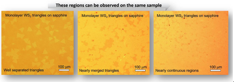
Isolated monolayer thickness WS2 are grown onto c-cut (0001) sapphire substrates. This particular product contains monolayer thickness WS2 triangular flakes randomly distributed across sapphire substrate. While some regions reach continuity with coalesced WS2 triangles, this sample contains well-separated triangles for advanced spectroscopy, microscopy, and electronic measurements. Synthesized monolayer WS2 triangles are highly luminescent and Raman spectroscopy studies also confirm the monolayer thickness.
Sample Properties.
Sample size | 1cm x 1cm square shaped |
Substrate type | (0001) c-cut sapphire |
Coverage | Isolated and partially merged monolayer triangl |
Electrical properties | 2.0 eV Direct Bandgap Semiconductor |
Crystal structure | Hexagonal Phase |
Unit cell parameters | a = b = 0.312 nm, c = 1.230 nm, α = β = 90, γ = 120° |
Production method | Low pressure Chemical Vapor Deposition (LPCVD) |
Characterization methods | Raman, photoluminescence, TEM, EDS |
Specifications
1) Identification. Well-separated WS2 domains across c-cut sapphire
2) Physical dimensions. One centimeter in size. Larger sizes up to 2-inch wafer-scale available upon requests.
3) Smoothness. Atomically smooth surface with roughness < 0.2 nm.
4) Uniformity. Highly uniform surface morphology. WS2 triangles are scattered across sample.
5) Purity. 99.9995% purity as determined by nano-SIMS measurements
6) Reliability. Repeatable Raman and photoluminescence response
7) Crystallinity. High crystalline quality, Raman response, and photoluminescence emission comparable to single crystalline monolayer flakes.
8) Substrate. c-cut Sapphire but our research and development team can transfer WS2 triangles onto variety of substrates including PET, quartz, and SiO2/Si without significant compromising of material quality.
9) Defect profile. WS2 monolayer triangles do not contain intentional dopants or defects. However, our technical staff can produce defected WS2 using α-bombardment technique.
Supporting datasets [for 100% Full area coverage on SiO2/Si]
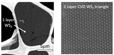
Transmission electron images (TEM) acquired from CVD grown WS2 (triangular) monolayers on c-cut sapphire confirming highly crystalline nature of monolayers
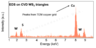
Energy dispersive X-ray spectroscopy (EDX) characterization on CVD grown full area coverage WS2 on sapphire confirming W:S 1:2 ratios
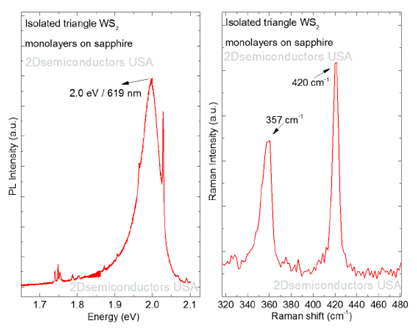
Room temperature photoluminescence spectroscopy (PL) and Raman spectroscopy (Raman) measurements performed on CVD grown full area coverage MoS2 monolayers on c-cut sapphire. Raman spectroscopy measurement confirm monolayer nature of the CVD grown samples and PL spectrum display sharp and bright PL peak located at 1.85 eV in agreement with the literature.

企业名称
上海巨纳科技有限公司
企业信息已认证
企业类型
信用代码
310109000501433
成立日期
2009-04-01
注册资本
1000
经营范围
通信设备、光电源、生物科技专业领域内的技术开发、技术转让、技术咨询、技术服务;销售仪器仪表,电子元器件,机械设备及配件,通信设备及相关产品(除卫星地面接收装置),日用百货,从事货物及技术的进出口业务。【企业经营涉及行政许可的,凭许可证件经营】
上海巨纳科技有限公司
公司地址
上海市虹口区宝山路778号海伦国际大厦5楼
客服电话
公司名称: 上海巨纳科技有限公司
公司地址: 上海市虹口区宝山路778号海伦国际大厦5楼 联系人: 袁文军 邮编: 200081
仪器信息网APP

展位手机站