产地类别: 国产
为您推荐相似的传感器/敏感元件
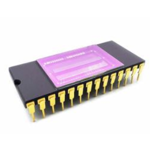
Near-Infrared Linear Image Sensor ( 0.9 – 1.7 μm ) with 512 x 1 pixels | ||
FEATURES ● 512 x 1 pixels [pixel size: S 25 x 25, M 25 x 250, L 25 x 500 μm] ● 28-pin Ceramic DIP (CDIP) ● Built-in Temperature Sensor ● 0.9 μm – 1.7 μm Spectral Range ● Minimum Pixel Operability > 99% ● Quantum Efficiency > 70% ● Snapshot ITR / IWR ● One output with up to 22 MHz Pixel Rate | APPLICATIONS ● Shortwave-Infrared Imaging ● Semiconductor Inspection / Process Monitoring ● Sorting / Recycling ● Near-Infrared Spectrophotometry | |
| The LDA512-C series is an uncooled near- infrared linear image sensor consisting of a linear InGaAs-detector array bonded on the p- on-n readout-IC. The series contains three products with different sensor pixel sizes. LDA512P25S-17-C, LDA512P25M-17-C, LDA512P25L-17-C. | |
GENERAL DESCRIPTIONS
Parameter | Unit | Value | |
Sensor Technology | --- | Planar InGaAs PIN | |
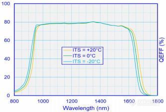
Spectral Range | μm | 0.9 – 1.7 | |
Actual Pixel Array | --- | 512 x 1 | |
Pixel Pitch | μm | 25 | |
Pixel Size | μm | Pixel Size | Dimension |
S | 25 x 25 | ||
M | 25 x 250 | ||
L | 25 x 500 | ||
Chip Size | mm | 15.3 x 4.5 | |
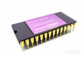
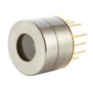
Package Type | --- | 28-pin Ceramic DIP (CDIP) |
Package Size L x W x T | mm | 35.56 x 15.61 x 7.15 |
Weight | g | 5.09 |
SPECIFICATIONS (1 ITS = 20 ± 1℃)
Parameter | Unit | Value | Conditions | ||
2.3 Dark Current | fA | S | ≤ 400 | Photo pixel biased @ -0.5 V | |
M | ≤ 600 | ||||
L | ≤ 1000 | ||||
2Quantum Efficiency * Fill Factor (QEFF) | % | ≥ 70 | λ = 1550 nm | ||
2 Response Nonuniformity | % | ≤ 5 | At 50% Full Well | ||
2 Response Nonlinearity | % | ≤ 2 | 15% – 85% Well Occupation Range | ||
Charge Capacity | Cint = 6.4 fF | μV/e- | 25 | 16 settings from 6.4 fF to 2.1 pF | |
Cint = 16 fF | 10 | ||||
Cint = 30 fF | 5.3 | ||||
Cint = 120 fF | 1.3 | ||||
Cint = 2.1 pF | 0.076 | ||||
Readout Noise | Cint = 6.4 fF | mV | 1.2 | ROIC Specifications | |
Cint = 16 fF | 0.8 | ||||
Cint = 30 fF | 0.6 | ||||
Cint = 120 fF | 0.5 | ||||
Cint = 2.1 pF | 0.25 | ||||
Output Swing | V | ≥ 2.0 | Gain @ 120 fF | ||
Minimum Integration Period | μs | 5 | ROIC Specifications | ||
Maximum Pixel Rate | MHz | 22 | ROIC Specifications | ||
2 Pixel Operability | % | ≥ 99 | Percentage of Pixels with QEFF Deviation within ± 20% *(QEFF Mean) | ||
1. Readings from Integrated Temperature Sensor (ITS).
2. These items are defined for central effective pixel array (512x1). Their values correspond to default operation conditions.
3. Medium gain, charge capacity @120fF, integration time 5ms.
ABSOLUTE MAXIMUM RATINGS
Parameter | Unit | Min. | Max. |
4Operating Temperature | ℃ | -40 | +70 |
4Storage Temperature | ℃ | -40 | +70 |
5 Power Consumption | mW | --- | 95 |
4. In non-condensing environment.
5. Without powering on the thermoelectric cooler.
PACKAGE OUTLINE (Unit: mm)
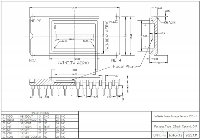
PIN DEFINITION | |||||||||
01 | VDD | 08 | SDOUT | 15 | GND | 22 | NC | ||
02 | RESET | 09 | DATVALID | 16 | NC | 23 | NC | ||
03 | NC | 10 | VOUT | 17 | NC | 24 | NC | ||
04 | INT | 11 | VDDA | 18 | VTEMP | 25 | NC | ||
05 | MC | 12 | VR2 | 19 | NC | 26 | NC | ||
06 | CEB | 13 | VR1 | 20 | NC | 27 | NC | ||
07 | SDIN | 14 | VDETCOM | 21 | NC | 28 | NC | ||
CHIP PROFILE
Layout
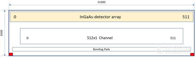
Chip size:15.3mm x 4.5mm
SPI Interface
LDA512 supports SPI protocol to set the command registers. There are functions of the gain mode, power consumption control and the sequence of pixel output.
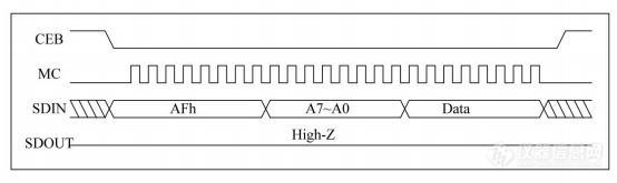
SPI Protocol Schematic
OPERATING CONDITIONS
Bias Input
Pin # | Bias | Voltage | Current | Remark | |
01 | VDD | 1.8 V | > 30 mA | Positive logic supply | |
11 | VDDA | 3.6 V | > 60 mA | Positive analog supply | |
12 | VR2 | 0.3 V | > 30 mA | External Input Bias | |
13 | VR1 | 2.3 V | > 5 mA | External Input Bias | |
14 | VDETCOM | > VR1 | -- | Detector common voltage 6 Detector bias = VDETCOM - VR1 | |
15 | GND | 0 V | -- | Ground | |
02 | RESET | 1.8 V | -- | Chip reset | |
6. VDETCOM lower than 2.3 V will forward bias the sensor, the exact zero bias voltage is device and temperature dependent.
Digital Pattern Input
Pin # | Clocks | Levels | Rise/Fall | Remark | |
04 | INT | 1.8 V / 0 V | < 50 nS | Integration time | |
05 | MC | 1.8 V / 0 V | < 5 nS | Master clock Max. Freq. = 22 MHz | |
06 | CEB | 1.8 V / 0 V | < 10 nS | 7Chip enable | |
07 | SDIN | 1.8 V / 0 V | < 5 nS | Data code input | |
7. The input and output of all commands start after the falling edge of CEB.
Digital Pattern Output
Pin # | Clocks | Levels | Rise/Fall | Remark | |
08 | SDOUT | 1.8 V / 0 V | -- | Data code output | |
09 | DATVALID | 1.8 V / 0 V | -- | Valid data output flag signal | |
Analog Output
Pin # | Outputs | Levels | Value | Remark | ||
10 | VOUT | 0.2 ~ 2.4 V | -- | Video output | ||
18 | VTEMP | 2.138 V | 27τ | Integrated Temperature Sensor (-0.6 mV /τ) | ||
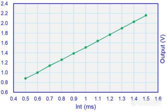
Output Linearity
Measurement Conditions | ||
Illumination | 1550 nm | |
Gain | @120 fF | |
Integration Time | 15 ~ 85% Well Occupation | |
0.5 ms ~ 1.4 ms | ||
ITS | 20 : 1℃ | |
Detector Bias | Vdetcom = 2.8 V (bias = -0.5 V) | |
Screen Size | 512 x 1 | |
QEFF Spectrum (typical example)
产品货期: 40天
整机质保期: 1年
培训服务: 安装调试现场免费培训
安装调试时间: 到货后3天内
电话支持响应时间: 1小时内
是否提供维保合同: 是
维修响应时间: 3天内
立鼎传感器LDA512P25X-17-C的工作原理介绍
传感器LDA512P25X-17-C的使用方法?
立鼎LDA512P25X-17-C多少钱一台?
传感器LDA512P25X-17-C可以检测什么?
传感器LDA512P25X-17-C使用的注意事项?
立鼎LDA512P25X-17-C的说明书有吗?
立鼎传感器LDA512P25X-17-C的操作规程有吗?
立鼎传感器LDA512P25X-17-C报价含票含运吗?
立鼎LDA512P25X-17-C有现货吗?