视频号

抖音号

哔哩哔哩号

前沿资讯手机看


分享到微信朋友圈
打开微信,点击底部的“发现”,
使用“扫一扫”即可将网页分享到朋友圈。
韩国帕克原子力显微镜于2018年在大中华区推出“帕克AFM奖学金”计划,由帕克原子力显微镜公司赞助,希望可以通过此次计划为年轻的科学家提供崭露头角的机会,并在纳米科学领域研究中注入新鲜的血液!2018年Park AFM奖学金的获得者是来自浙江大学物理系的王震博士,王博士通过使用Park NX10得到的相关研究成果写成论文“Defects controlled hole doping and multivalley transport in SnSe single crystals”发表于<
2019年,在众多使用Park AFM发出研究成果论文的申请者中,以色列理工学院博士后惠飞博士在提及Park NX-Hivac的论文"Scanning probe microscopy for advanced nanoelectronics"被<<Nature Electronics>>收录,成为2019 Park AFM奖学金的第一位获得者。

Park NX-Hivac于2018年12月10日被首次引进广东以色列理工学院(GTIIT),惠飞博士后的导师Mario Lanza教授是利用SPM进行纳米电学测试方面公认的专家。
在论文中,惠飞博士后指出“随着电子器件尺寸的不断缩小,具有能够精确探测局部性质的表征方法变得越来越重要。扫描探针显微镜技术可以检测局部现象,尤其是导电原子力显微镜可以研究材料的局部机电性质。这些表征已经在纳米电子学的发展中起到了重要的作用,但是在于探针台(通常用于测试电子器件)相比,它们的能力仍然相对有限。在此论文中,讨论了导电原子力显微镜在纳米电子学中的潜能,并探索可能的表征策略,增强的电子学技术以及改进的多探针测试方法。同时,作者还提出了一种多探针扫描探针显微镜系统,它结合了不同类型的探针,可以在真空条件下同时进行纳米加工和表征实验。”

惠飞博士后的个人专访即将被收录到最新一期的NanoScientific杂志中,以下为惠飞博士后的专访原文:
Fei Hui is currently a postdoctoral fellow inTechnion-Israel Institute of Technology, she received her PhD degree from the Universityof Barcelona in 2018. During her PhD, Dr. Hui was a visiting scholar atMassachusetts Institute of Technology (USA) for 12 months, where she learnedchemical vapor deposition two-dimensional (2D) materials (e.g. hexagonal boronnitride, graphene) on different substrates (i.e. Cu, Pt, Fe and Ni). She alsoreceived the Researcher Mobility Grant from Royal Society of Chemistry, whichsupported her studies at the University of Cambridge (UK) for 6 months. In theCambridge Graphene Center, she learned how to synthesize graphene oxide thinfilms and, more interestingly, how to cover nanoprobes with thin films of thismaterial via spray technique. She has published over 40 research papers (11papers are as first-author) on top journals of Nature Electronic, AdvancedFunctional Materials, ACS Applied Materials and Interfaces, 2D Materials (amongothers), and with more than 811 citations indicated by Google Scholar (https://scholar.google.com/citations?user=Ht0HvKYAAAAJ&hl=en&oi=ao). She has applied for two internationalpatents, and one of them (cost-effective fabrication of ultra-durable graphenecoated nanoprobes) attracted around $1 million investment.
Interview questions采访问题:
1. Please summarize theresearch you do and explain why it is significant?
My research topic is the development oftwo-dimensional (2D) materials based electronic devices. We are aiming tointegrate 2D materials (e.g. hexagonal boron nitride, graphene or molybdenumdisulfide) into electronic devices (e.g. memristors or field effecttransistors). Due to the atomic thin layer and extraordinary properties (e.g.high thermal and electrical conductivity, flexibility and transparency) of 2Dmaterials, it allows us to design miniaturized devices, which exhibit someexotic performances that conventional transition metal oxides (e.g. HfO2)-baseddevices do not show. More specifically, I firstly synthesis monolayer ormultilayer 2D materials using chemical vapor deposition (CVD) methodology. Aftergrowth I used several techniques to analyze the quality of these materials,mainly Raman Spectroscopy and cross-sectional transmission electron microscopy(X-TEM), but the technique that provided me best results was conductive atomicforce microscopy (CAFM). Using this technique, I explored the dielectricproperties of hexagonal boron nitride (h-BN) and graphene oxide (GO), includingtunneling current, charge trapping, trap-assisted tunneling, stress-inducedleakage current, dielectric breakdown and resistive switching (RS). I also usedthese 2D materials to fabricate memristive devices, and analyzed them using aprobestation connected to a semiconductor parameter analyzer (working indifferent atmospheres).
2. How might yourresearch be used?
In my work, I employed a scalable CVD technique tosynthesis large size of 2D materials, which allow us to fabricate high-yield electronicdevices and study their device-to-device variability. Moreover, this methodologyis more compatible with and useful for the industry than single/few devicesfabricated by mechanical exfoliation. In our previous work, we have proved thath-BN can be used as a RS medium and the metal/h-BN/metal devices showed both volatileand non-volatile RS behaviors, enabling the emulation of a range of synaptic-likebehavior, including both short- and long- term plasticity. Therefore, ourresearch would accelerate the use of 2D materials for building futurewafer-scale and high-density electronic memories and/or artificial neuralnetworks.
3. What features of Park AFMare the most beneficial and why?
Park AFM system is a powerful tool that provides uswith more accurate and reliable information under different conditions (ambientand vacuum conditions), which is extremely important for the research field ofnanoscience. First of all, the true non-contact mode allows us to acquire thetopographic information, such as the wrinkles of 2D materials or some tinyparticles, without the damage of probes and surface modification of specimens. Second,the image/position drift is negligible, we can perform spectroscopymeasurements (e.g. current vs. voltage, force vs. distance) at specificlocation or in a matrix pattern and then go back to them exactly. Moreover, thenavigation and the software interface are quite user-friendly, which save usmuch more time.
4. Why is the Park AFMimportant for your research?
This Park NX-Hivac system is able to simultaneouslyperform four tasks that are essential to study RS reliably: i) measure currentsin tapping mode (to avoid premature tip wearing and material damage), ii)measure high currents from picoamperes to miliamperes in both polarities byusing a logarithmic preamplifier (to monitor the set/reset transitions insitu), iii) measure in high vacuum up to 10-6 torr (to avoid localanodic oxidation and unwanted moisture-related reactions), and iv) measure athigh temperatures up to 600 oC (not only to study reliability, but also toevaporate all water molecules on the materials after pumping the vacuum). Theneed of these four features to reliably measure RS at the nanoscale isextensively described in the book (Conductive Atomic Force Microscopy:Applications in Nanomaterials, ISBN: 978-3-527-69978-0, Wiley-VCH Weinheim,Germany, 2017) edited by Prof. Mario Lanza, who is aleading expert in CAFM science, and there is no other equipment in the worldthat can carry out all these actions simultaneously. The use of this tool willbe a high advantage compared to other groups.

Park另一位奖学金获得者是来自天津大学纳米材料与技术研究中心研究团队的王燕燕研究员,王燕燕研究员通过使用Park NX10写出以“One-Step Fabrication of Ultralow Pt Loading High Efficiency Proton Exchange Membrane for Water Electrolysis by Conventional E-Beam Metal Deposition”为标题的论文并收录在“Advanced Sustainable Systems”期刊中。
[来源:Park帕克原子力显微镜]
积极响应国家利好政策: Park Systems 支持设备更新,助力节能提效
2024.04.01
喜迎国家减税新策,力掀仪器申购浪潮 I Park原子力显微镜为您提供最佳解决方案
2022.10.14

2022.07.25


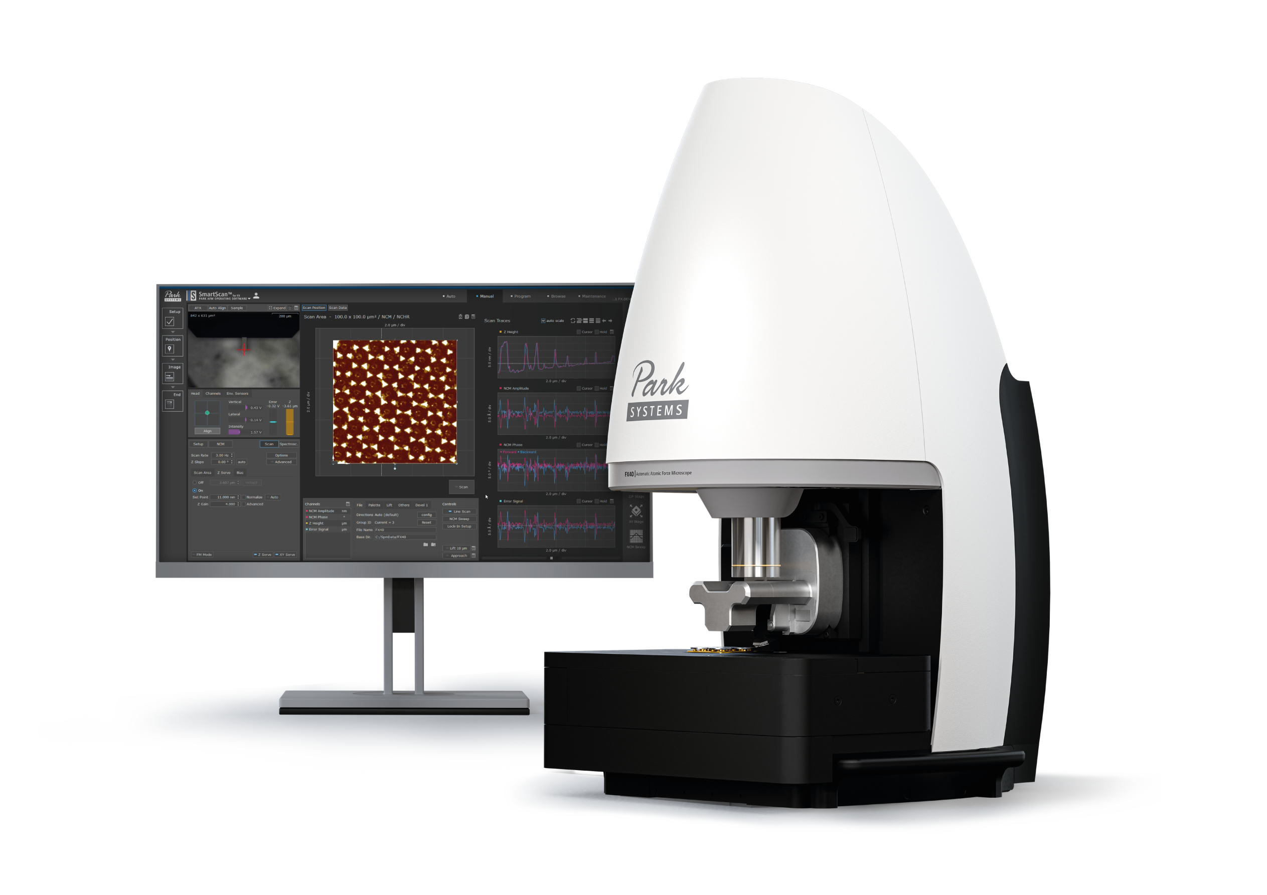
Park FX40:一款高智能全新型自动化原子力显微镜重磅来袭
2022.07.07
品牌合作伙伴


版权与免责声明:
① 凡本网注明"来源:仪器信息网"的所有作品,版权均属于仪器信息网,未经本网授权不得转载、摘编或利用其它方式使用。已获本网授权的作品,应在授权范围内使用,并注明"来源:仪器信息网"。违者本网将追究相关法律责任。
② 本网凡注明"来源:xxx(非本网)"的作品,均转载自其它媒体,转载目的在于传递更多信息,并不代表本网赞同其观点和对其真实性负责,且不承担此类作品侵权行为的直接责任及连带责任。如其他媒体、网站或个人从本网下载使用,必须保留本网注明的"稿件来源",并自负版权等法律责任。
③ 如涉及作品内容、版权等问题,请在作品发表之日起两周内与本网联系,否则视为默认仪器信息网有权转载。
![]() 谢谢您的赞赏,您的鼓励是我前进的动力~
谢谢您的赞赏,您的鼓励是我前进的动力~
打赏失败了~
评论成功+4积分
评论成功,积分获取达到限制
![]() 投票成功~
投票成功~
投票失败了~